

Page 1
General Description
The MAX9205/MAX9207 serializers transform 10-bitwide parallel LVCMOS/LVTTL data into a serial highspeed bus low-voltage differential signaling (LVDS)
data stream. The serializers typically pair with deserializers like the MAX9206/MAX9208, which receive the
serial output and transform it back to 10-bit-wide parallel data.
The MAX9205/MAX9207 transmit serial data at speeds
up to 400Mbps and 660Mbps, respectively, over PCB
traces or twisted-pair cables. Since the clock is recovered from the serial data stream, clock-to-data and
data-to-data skew that would be present with a parallel
bus are eliminated.
The serializers require no external components and few
control signals. The input data strobe edge is selected
by TCLK_R/F. PWRDN is used to save power when the
devices are not in use. Upon power-up, a synchronization mode is activated, which is controlled by two SYNC
inputs, SYNC1 and SYNC2.
The MAX9205 can lock to a 16MHz to 40MHz system
clock, while the MAX9207 can lock to a 40MHz to
66MHz system clock. The serializer output is held in
high impedance until the device is fully locked to the
local system clock, or when the device is in powerdown mode.
Both the devices operate from a single +3.3V supply,
are specified for operation from -40°C to +85°C, and
are available in 28-pin SSOP packages.
Applications
Features
o Standalone Serializer (vs. SERDES) Ideal for
Unidirectional Links
o Framing Bits for Deserializer Resync Allow Hot
Insertion Without System Interruption
o LVDS Serial Output Rated for Point-to-Point and
Bus Applications
o Wide Reference Clock Input Range
16MHz to 40MHz (MAX9205)
40MHz to 66MHz (MAX9207)
o Low 140ps (pk-pk) Deterministic Jitter (MAX9207)
o Low 34mA Supply Current (MAX9205)
o 10-Bit Parallel LVCMOS/LVTTL Interface
o Up to 660Mbps Payload Data Rate (MAX9207)
o Programmable Active Edge on Input Latch
o Pin-Compatible Upgrades to DS92LV1021 and
DS92LV1023
MAX9205/MAX9207
10-Bit Bus LVDS Serializers
________________________________________________________________
Maxim Integrated Products
1
Ordering Information
19-2029; Rev 1; 11/10
For pricing, delivery, and ordering information, please contact Maxim Direct at 1-888-629-4642,
or visit Maxim’s website at www.maxim-ic.com.
EVALUATION KIT
AVAILABLE
Pin Configuration and Functional Diagram appear at end of
data sheet.
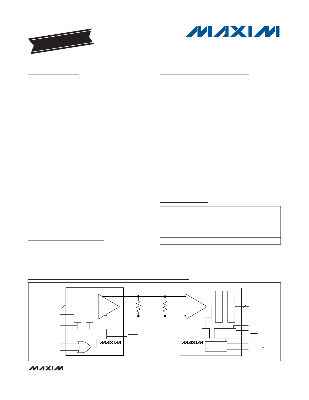
Typical Application Circuit
Cellular Phone Base
Stations
Add Drop Muxes
Digital Cross-Connects
DSLAMs
Network Switches and
Routers
Backplane Interconnect
+
Denotes a lead(Pb)-free/RoHS-compliant package.
/V denotes an automotive qualified part.
PART
MAX9205EAI+ -40°C to +85°C 28 SSOP 16 to 40
M AX 9205E AI/V + -40°C to +85°C 28 SSOP 16 to 40
MAX9207EAI+ -40°C to +85°C 28 SSOP 40 to 66
TEMP
RANGE
PINPACKAGE
REF CLOCK
RANGE
(MHz)
BUS
OUT+
IN_
TCLK_R/F
TCLK
SYNC 1
SYNC 2
10
INPUT LATCH
PARALLEL-TO-SERIAL
TIMING AND
PLL
CONTROL
MAX9205
MAX9207
100Ω 100Ω
OUT-
EN
PWRDN
LVDS
PCB OR
TWISTED PAIR
IN+
10
OUT_
IN-
TIMING AND
PLL
MAX9206
MAX9208
CLOCK
RECOVERY
OUTPUT LATCH
SERIAL-TO-PARALLEL
CONTROL
REFCLK
EN
LOCK
RCLK
RCLK_R/F
Page 2
MAX9205/MAX9207
10-Bit Bus LVDS Serializers
2 _______________________________________________________________________________________
ABSOLUTE MAXIMUM RATINGS
DC ELECTRICAL CHARACTERISTICS
(V
AVCC
= V
DVCC
= +3.0V to +3.6V, RL= 27Ω ±1% or 50Ω ±1%, CL= 10pF, TA= -40°C to +85°C. Typical values are at V
AVCC
=
V
DVCC
= +3.3V and TA= +25°C, unless otherwise noted.) (Notes 1, 2, 3)
Stresses beyond those listed under “Absolute Maximum Ratings” may cause permanent damage to the device. These are stress ratings only, and functional
operation of the device at these or any other conditions beyond those indicated in the operational sections of the specifications is not implied. Exposure to
absolute maximum rating conditions for extended periods may affect device reliability.
AVCC, DVCC to GND..........................……………-0.3V to +4.0V
IN_, SYNC1, SYNC2, EN, TCLK_R/F, TCLK,
PWRDN to GND......................................-0.3V to (V
CC
+ 0.3V)
OUT+, OUT- to GND .............................................-0.3V to +4.0V
Output Short-Circuit Duration.....................................Continuous
Continuous Power Dissipation (T
A
= +70°C)
28-Pin SSOP (derate 9.5mW/°C above +70°C) ..........762mW
Storage Temperature Range .............................-65°C to +150°C
Junction Temperature......................................................+150°C
Operating Temperature Range ...........................-40°C to +85°C
ESD Protection (Human Body Model, OUT+, OUT-) ...........±8kV
Lead Temperature (soldering, 10s) .................................+300°C
Soldering Temperature (reflow) .......................................+260°C
PARAMETER SYMBOL CONDITIONS MIN TYP MAX UNITS
LVCMOS/LVTLL LOGIC INPUTS (IN0 TO IN9, EN, SYNC1, SYNC2, TCLK, TCLK_R/F, PWRDN)
High-Level Input Voltage V
Low-Level Input Voltage V
Input Current I
IH
IL
V
IN
= 0V or V
IN_
BUS LVDS OUTPUTS (OUT+, OUT-)
Differential Output Voltage V
Change in VOD Between
Complementary Output States
ΔV
Output Offset Voltage V
Change in V
Complementary Output States
Between
OS
ΔV
Output Short-Circuit Current I
Output High-Impedance Current I
Power-Off Output Current I
OD
OS
OS
OZ
OX
Figure 1
Figure 1 1 35 mV
OD
Figure 1 0.9 1.15 1.3 V
Figure 1 3 35 mV
OS
V
or V
OUT+
IN0 to IN9 = PWRDN = EN = high
V
V
V
PWRDN
OUT+
_VCC
or V
= 0V, V
or VEN = 0.8V,
POWER SUPPLY
RL = 27_ or 50_
Supply Current I
CC
worst-case pattern
(Figures 2, 4)
Power-Down Supply Current I
CCX
PWRDN = low 8 mA
2.0 V
GND 0.8 V
-20 +20 µA
-13 -15 mA
-10 +10 µA
OUT-
OUT-
_VCC
= 0V,
= 0V or V
or V
OUT+
R
= 27Ω 200 286 400 mV
L
R
= 50Ω 250 460 600 mV
L
_VCC
= 0V or 3.6V -10 +10 µA
OUT-
MAX9205
MAX9207
16MHz 23 35
40MHz 34 45
40MHz 32 50
66MHz 45 60
CC
mA
V
Page 3
MAX9205/MAX9207
10-Bit Bus LVDS Serializers
_______________________________________________________________________________________ 3
AC ELECTRICAL CHARACTERISTICS
(V
AVCC
= V
DVCC
= +3.0V to +3.6V, RL= 27Ω ±1% or 50Ω ±1%, CL= 10pF, TA= -40°C to +85°C. Typical values are at V
AVCC
=
V
DVCC
= +3.3V and TA= +25°C, unless otherwise noted.) (Notes 2, 4)
PARAMETER SYMBOL CONDITIONS MIN TYP MAX UNITS
TRANSMIT CLOCK (TCLK) TIMING REQUIREMENTS
TCLK Center Frequency f
TCCF
MAX9205 16 40 MHz
MAX9207 40 66 MHz
TCLK Frequency Variation TCFV -200 200 ppm
TCLK Period t
TCP
MAX9205 25 62.5
MAX9207 15.15 25
ns
TCLK Duty Cyc le TCDC 40 60 %
TCLK Input Transition Time t
TCLK Input Jitter t
Figure 3 3 6 ns
CLKT
150
JIT
ps
(RMS)
SWITCHING CHARACTERISTICS
Low-to-High Tran sition Time t
High-to-Low Tran sition Time t
Figure 4
LHT
Figure 4
HLT
RL = 27 150 300 400
R
= 50 150 350 500
L
RL = 27 150 300 400
= 50 150 350 500
R
L
ps
ps
IN_ Setup to TCLK tS Figure 5 1 ns
IN_ Hold from TCLK tH Figure 5 3 ns
OUTPUT High State to HighImpedance Dela y
OUTPUT Low State to HighImpedance Dela y
OUTPUT High Impedance to
High-State Delay
OUTPUT High Impedance to
Low-State Delay
SYNC Pulse Width t
PLL Lock Time tPL Figure 7
Bus LVDS Bit Width t
Serializer Delay tSD Figure 8 t
Figures 6, 7 4.5 10 ns
t
HZ
Figures 6, 7 4.5 10 ns
t
LZ
Figures 6, 7 4.5 10 ns
t
ZH
Figures 6, 7 4.5 10 ns
t
ZL
6 x t
SPW
t
BIT
ns
TCP
2048 x
t
TCP
/ 6
TCP
TCP
2049 x
t
TCP
/12 ns
(t
TCP
+ 5
/6)
ns
ns
Page 4

MAX9205/MAX9207
10-Bit Bus LVDS Serializers
4 _______________________________________________________________________________________
Typical Operating Characteristics
(V
AVCC
= V
DVCC
= +3.3V, RL= 27Ω, CL = 10pF, TA = +25°C, unless otherwise noted.)
10
30
20
40
50
3.0 3.3 3.6
WORST-CASE PATTERN SUPPLY CURRENT
vs. SUPPLY VOLTAGE
MAX9205 toc01
SUPPLY VOLTAGE (V)
SUPPLY CURRENT (mA)
TCLK = 40MHz
MAX9205
10
30
20
40
50
3.0 3.3 3.6
WORST-CASE PATTERN SUPPLY CURRENT
vs. SUPPLY VOLTAGE
MAX9205 toc01
SUPPLY VOLTAGE (V)
SUPPLY CURRENT (mA)
TCLK = 40MHz
MAX9205
AC ELECTRICAL CHARACTERISTICS (continued)
(V
AVCC
= V
DVCC
= +3.0V to +3.6V, RL= 27Ω ±1% or 50Ω ±1%, CL= 10pF, TA= -40°C to +85°C. Typical values are at V
AVCC
=
V
DVCC
= +3.3V and TA= +25°C, unless otherwise noted.) (Notes 2, 4)
Note 1: Current into a pin is defined as positive. Current out of a pin is defined as negative. All voltages are referenced to ground
except V
OD
, ΔVOD, and VOS.
Note 2: CLincludes scope probe and test jig capacitance.
Note 3: Parameters 100% tested at T
A
= +25°C. Limits over operating temperature range guaranteed by design and characterization.
Note 4: AC parameters are guaranteed by design and characterization.
Determinist ic Jitter (Figure 9) t
Random Jitter (Figure 10) t
PARAMETER SYMBOL CONDITIONS MIN TYP MAX UNITS
MAX9205
DJIT
MAX9207
MAX9205
RJIT
MAX9207
16MHz 200
40MHz 140
40MHz 140
66MHz 140
16MHz 13
40MHz 9
40MHz 9
66MHz 6
ps
(pk-pk)
ps
(RMS)
Page 5

MAX9205/MAX9207
10-Bit Bus LVDS Serializers
_______________________________________________________________________________________ 5
Pin Description
Detailed Description
The MAX9205/MAX9207 are 10-bit serializers designed
to transmit data over balanced media that may be a
standard twisted-pair cable or PCB traces at 160Mbps
to 660Mbps. The interface may be double-terminated
point-to-point or a heavily loaded multipoint bus. The
characteristic impedance of the media and connected
devices can range from 100Ω for a point-to-point interface to 54Ω for a heavily loaded multipoint bus. A double-terminated point-to-point interface uses a
100Ω-termination resistor at each end of the interface,
resulting in a load of 50Ω. A heavily loaded multipoint
bus requires a termination as low as 54Ω at each end
of the bus, resulting in a termination load of 27Ω. The
serializer requires a deserializer such as the
MAX9206/MAX9208 for a complete data transmission
application.
A high-state start bit and a low-state stop bit, added
internally, frame the 10-bit parallel input data and
ensure a transition in the serial data stream. Therefore,
12 serial bits are transmitted for each 10-bit parallel
input. The MAX9205 accepts a 16MHz to 40MHz reference clock, producing a serial data rate of 192Mbps
(12 bits x 16MHz) to 480Mbps (12 bits x 40MHz). The
MAX9207 accepts a 40MHz to 66MHz reference clock,
producing 480Mbps to 792Mbps. However, since only
10 bits are from input data, the actual throughput is 10
times the TCLK frequency.
To transmit data, the serializers sequence through
three modes: initialization mode, synchronization mode,
and data transmission mode.
PIN NAME FUNCTION
LVCMOS/LVTTL Logic Inputs. The two SYNC pins are ORed. When at least one of the two pins
are asserted high for at least six cycles of TCLK, the serializer initiates a transmission of 1024
1, 2
3–12 IN0–IN9 LVCMOS/LVTTL Data Inputs. Data is loaded into a 10-bit latch by the selected TCLK edge.
13 TCLK_R/F
14 TCLK
15, 16 DGND Digital Circuit Ground. Connect to ground plane.
17, 26 AVCC
18, 20,
23, 25
19 EN
21 OUT- Inverting Bus LVDS Differential Output
22 OUT+ Noninverting Bus LVDS Differential Output
24 PWRDN
27, 28 DVCC
SYNC 1,
SYNC 2
AGND Analog Circuit Ground. Connect to ground plane.
SYNC patterns. If held high after 1024 SYNC patterns have been transmitted, SYNC patterns
continue to be sent until the SYNC pin is asserted low. Toggling a SYNC pin after six TCLK cycles
high and before 1024 SYNC patterns have been transmitted does not affect the output of the 1024
SYNC patterns.
LVCMOS/LVTTL Logic Input. High selects a TCLK rising-edge data strobe. Low selects a TCLK
falling-edge data strobe.
LVCMOS/LVTTL Reference Clock Input. The MAX9205 accepts a 16MHz to 40MHz clock. The
MAX9207 accepts a 40MHz to 66MHz clock. TCLK provides a frequency reference to the PLL and
strobes parallel data into the input latch.
Analog Circuit Power Supply (Includes PLL). Bypass AVCC to ground with a 0.1µF capacitor and a
0.001µF capacitor. Place the 0.001µF capacitor closest to AVCC.
LVCMOS/LVTTL Logic Input. High enables serial data output. Low puts the bus LVDS output into
high impedance.
LVCMOS/LVTTL Logic Input. Low puts the device into power-down mode and the output into high
impedance.
Digital Circuit Power Supply. Bypass DVCC to ground with a 0.1µF capacitor and a 0.001µF
capacitor. Place the 0.001µF capacitor closest to DVCC.
Page 6

MAX9205/MAX9207
Initialization Mode
When VCCis applied, the outputs are held in high
impedance and internal circuitry is disabled by on-chip
power-on-reset circuitry. When the supply voltage
reaches 2.35V, the PLL starts to lock to a local reference clock (16MHz to 40MHz for MAX9205 and 40MHz
to 66MHz for MAX9207). The reference clock, TCLK, is
provided by the system. A serializer locks within 2049
cycles of TCLK. Once locked, a serializer is ready to
send data or SYNC patterns depending on the levels of
SYNC 1 and SYNC 2.
Synchronization Mode
To rapidly synchronize with a deserializer, SYNC patterns can be sent. A SYNC pattern is six consecutive
ones followed by six consecutive zeros repeating every
TCLK period. When one or both SYNC inputs are
asserted high for at least six cycles of TCLK, the serializer will initiate the transmission of 1024 SYNC patterns.
The serializer will continue to send SYNC patterns if
either of the SYNC input pins remains high. Toggling
one SYNC input with the other SYNC input low before
1024 SYNC patterns are output does not interrupt the
output of the 1024 SYNC patterns.
Data Transmission Mode
After initialization, both SYNC input pins must be set
low by users or through a control signal from the deserializer before data transmission begins. Provided that
SYNC inputs are low, input data at IN0–9 are clocked
into the serializer by the TCLK input. Setting TCLK_R/F
high selects the rising edge of TCLK for data strobe
and low selects the falling edge. If either of the SYNC
inputs goes high for six TCLK cycles at any time during
data transmission, the data at IN0–9 are ignored and
SYNC patterns are sent for at least 1024 TCLK cycles.
A start bit high and a stop bit low frame the 10-bit data
and function as the embedded clock edge in the serial
data stream. The serial rate is the TCLK frequency
times the data and appended bits. For example, if
TCLK is 40MHz, the serial rate is 40 x 12 (10 + 2 bits) =
480Mbps. Since only 10 bits are from input data, the
payload rate is 40 x 10 = 400Mbps.
Power-Down
Power-down mode is entered when the PWRDN pin is
driven low. In power-down mode, the PLL of the serializer is stopped and the outputs (OUT+ and OUT-) are
in high impedance, disabling drive current and also
reducing supply current. When PWRDN is driven high,
the serializer must reinitialize and resynchronize before
data can be transferred.
High-Impedance State
The serializer output pins (OUT+ and OUT-) are held in
high impedance when the supply voltage is first
applied and while the PLL is locking to the local reference clock. Setting EN or PWRDN low puts the device
in high impedance. After initialization, EN functions
asynchronously. For example, the serializer output can
be put into high impedance while SYNC patterns are
being sent without affecting the internal timing of the
SYNC pattern generation. However, if the serializer
goes into high impedance, a deserializer loses PLL
lock and needs to resynchronize before data transfer
can resume.
10-Bit Bus LVDS Serializers
6 _______________________________________________________________________________________
Table 1. Input /Output Function Table
X = Don’t care.
INPUTS OUTPUTS
EN PWRDN SYNC 1 SYNC 2 OUT+, OUT-
When either or both SYNC 1
HH
HH L L
XL X X
LX X X
and SYNC 2 are held high for
at least six TCLK cycles
Synchronization Mode. SYNC patterns of six 1s and six 0s are
transmitted every TCLK cycle for at least 1024 TCLK cycles.
Data at IN0–9 are ignored.
Data Transmission Mode. IN0–9 and 2 frame bits are
transmitted every TCLK cycle.
Output in high-impedance.
Page 7

Applications Information
Power-Supply Bypassing
Bypass AVCC with high-frequency surface-mount
ceramic 0.1µF and 0.001µF capacitors in parallel as
close to the device as possible, with the smaller valued
capacitor closest to AVCC. Bypass DVCC with high-frequency surface-mount ceramic 0.1µF and 0.001µF
capacitors in parallel as close to the device as possible, with the smaller valued capacitor closest to DVCC.
Differential Traces and Termination
Output trace characteristics affect the performance of
the MAX9205/MAX9207. Use controlled-impedance
media and terminate at both ends of the transmission
line in the media's characteristic impedance.
Termination with a single resistor at the end of a pointto-point link typically provides acceptable performance.
However, the MAX9205/MAX9207 output levels are
specified for double-terminated point-to-point and multipoint applications. With a single 100Ω termination, the
output swing is larger.
Avoid the use of unbalanced cables such as ribbon or
simple coaxial cable. Balanced cables such as twisted
pair offer superior signal quality and tend to generate
less EMI due to canceling effects. Balanced cables
tend to pick up noise as common mode, which is
rejected by a differential receiver.
Eliminate reflections and ensure that noise couples as
common mode by running the differential traces close
together. Reduce skew by matching the electrical
length of the traces. Excessive skew can result in a
degradation of magnetic field cancellation.
The differential output signals should be routed close to
each other to cancel their external magnetic field.
Maintain a constant distance between the differential
traces to avoid discontinuities in differential impedance.
Avoid 90° turns and minimize the number of vias to further prevent impedance discontinuities.
MAX9205/MAX9207
10-Bit Bus LVDS Serializers
_______________________________________________________________________________________ 7
Figure 1. Output Voltage Definitions
Figure 2. Worst-Case ICCTest Pattern
Figure 3. Input Clock Transition Time Requirement
R
OUT+
V
OUT-
L
2
OD
V
R
2
OS
L
TCLK
ODD IN_
EVEN IN_
TCLK
10%
90%
t
CLKT
TCLK_R/F = LOW
3V
0
t
CLKT
90%
10%
Page 8

MAX9205/MAX9207
10-Bit Bus LVDS Serializers
8 _______________________________________________________________________________________
Figure 4. Output Load and Transition Times
Figure 5. Data Input Setup and Hold Times
Figure 6. High-Impedance Test Circuit and Timing
OUT+
OUT-
10pF
10pF
V
= (OUT+) - (OUT-)
DIFF
R
L
TCLK
IN_
TIMING SHOWN FOR TCLK_R/F = LOW
1.5V
80%
DIFF
20%
1.5V
t
t
LHT
S
PARASITIC PACKAGE AND
TRACE CAPACITANCE
t
TCP
t
H
1.5V
V
80%
V
= 0
DIFF
20%
t
HLT
1.5V1.5V
EN
OUT±
OUT+
OUT-
EN
3V
1.5V
0
V
OH
V
OL
t
HZ
t
LZ
10pF
10pF
13.5Ω
13.5Ω
1.5V
+1.1V
t
ZH
50%50%
t
ZL
50%50%
1.1V
1.1V
Page 9

MAX9205/MAX9207
10-Bit Bus LVDS Serializers
_______________________________________________________________________________________ 9
PWRDN
Figure 7. PLL Lock Time and PWRDN High-Impedance Delays
Figure 8. Serializer Delay
Figure 9. Definition of Deterministic Jitter (t
DJIT
)
Figure 10. Definition of Random Jitter (t
RJIT
)
2.0V
0.8V
t
PL
TCLK
OUT±
SYNC 1 = SYNC 2 = LOW
EN = HIGH
TCLK_R/F = HIGH
IN
TCLK
OUT±
IN0 - IN9 SYMBOL N
t
SD
1.5V
TIMING SHOWN FOR TCLK_R/F = HIGH
START BIT
OUT0 - OUT9 SYMBOL N
1.5V
tZH OR t
ZL
IN0 - IN9 SYMBOL N + 1
STOP BIT START BIT STOP BIT
ACTIVE
t
OR t
HZ
LZ
HIGH IMPEDANCEHIGH IMPEDANCE
OUT0 - OUT9 SYMBOL N+1
(OUT+) - (OUT-)
WAVEFORM
t
DJIT
SUPERIMPOSED RANDOM DATA
V
= 0 V
DIFF
O DIFFERENTIAL
= (OUT+) - (OUT-)TCLK_ R/F = HIGH
DIFF
(OUT+) - (OUT-)
WAVEFORM
O DIFFERENTIAL
t
RJIT
t
RJIT
"CLOCK" PATTERN (1010...)
Page 10

MAX9205/MAX9207
10-Bit Bus LVDS Serializers
10 ______________________________________________________________________________________
Topologies
The serializers can operate in a variety of topologies.
Examples of double-terminated point-to-point, multidrop, point-to-point broadcast, and multipoint topologies are shown in Figures 11 through 14. Use 1%
surface-mount termination resistors.
A point-to-point connection terminated at each end in
the characteristic impedance of the cable or PCB
traces is shown in Figure 11. The total load seen by the
serializer is 50Ω. The double termination typically
reduces reflections compared to a single 100Ω termi-
nation. A single 100Ω termination at the deserializer
input is feasible and will make the differential signal
swing larger.
A serializer located at one end of a backplane bus driving multiple deserializers in a multidrop configuration
is shown in Figure 12. A 54Ω resistor at the far end terminates the bus. This topology allows “broadcast” of
data with a minimum of interconnect.
Figure 11. Double-Terminated Point-to-Point
Figure 12. Multidrop
PARALLEL
DATA IN
100Ω
MAX9205
MAX9207
SERIALIZED DATA
100Ω
MAX9206
MAX9208
PARALLEL
DATA OUT
ASIC ASIC ASIC ASIC
MAX9206
MAX9208
MAX9206
MAX9208
MAX9206
MAX9208
MAX9205
MAX9207
ASIC
MAX9206
MAX9208
54Ω
Page 11

MAX9205/MAX9207
10-Bit Bus LVDS Serializers
______________________________________________________________________________________ 11
Figure 13. Point-to-Point Broadcast Using MAX9150 Repeater
A point-to-point version of the multidrop bus is shown in
Figure 13. The low-jitter MAX9150 10-port repeater is
used to reproduce and transmit the serializer output
over 10 double-terminated point-to-point links.
Compared to the multidrop bus, more interconnect is
traded for more robust hot-plug capability.
The repeater eliminates nine serializers compared to 10
individual point-to-point serializer-to-deserializer connections. Since repeater jitter subtracts from the serializer-deserializer timing margin, a low-jitter repeater is
essential in most high data rate applications.
Multiple serializers and deserializers bused over a differential serial connection on a backplane are shown in
Figure 14. The second serializer can be a backup to
the primary serializer. The typical close spacing (1in or
less) of cards on a backplane reduces the characteristic impedance by as much as half the initial, unloaded
value. Termination resistors that match the loaded characteristic impedance are required at each end of the
bus. The total loaded seen by the serializer is 27Ω in
this case.
Board Layout
For bus LVDS applications, a four-layer PCB that provides separate power, ground, and input/output signals
is recommended. Separate LVTTL/LVCMOS and bus
LVDS signals from each other to prevent coupling into
the bus LVDS lines.
ASIC
MAX9205
MAX9207
MAX9150
REPEATER
100Ω
100Ω
ASIC ASIC
MAX9206
MAX9208
100Ω
100Ω
MAX9206
MAX9208
Page 12

MAX9205/MAX9207
10-Bit Bus LVDS Serializers
12 ______________________________________________________________________________________
Functional DiagramPin Configuration
Figure 14. Multipoint
Package Information
For the latest package outline information and land patterns,
go to www.maxim-ic.com/packages
. Note that a “+”, “#”, or
“-” in the package code indicates RoHS status only. Package
drawings may show a different suffix character, but the drawing
pertains to the package regardless of RoHS status.
PACKAGE
TYPE
PACKAGE
CODE
OUTLINE
NO.
LAND
PATTERN NO.
28 SSOP A28+4
21-0056 90-0095
Chip Information
PROCESS: CMOS
ASIC
MAX9205
MAX9207
54Ω
ASIC ASIC ASIC ASIC
MAX9205
MAX9207
TOP VIEW
+
1
2
3
4
5
6
7
8
9
10
11
12
13
14
SYNC1
SYNC2
IN0
IN1
IN2
IN3
IN4
IN5
IN6
IN7
IN8
IN9
TCLK_R/F
TCLK
MAX9205
MAX9207
SSOP
DVCC
DVCC
AVCC
AGND
PWRDN
AGND
OUT+
OUT-
AGND
AGND
AVCC
DGND
DGND
28
27
26
25
24
23
22
21
20
19
EN
18
17
16
15
MAX9206
MAX9208
MAX9206
MAX9208
MAX9206
MAX9208
54Ω
IN_
TCLK_R/F
TCLK
SYNC 1
SYNC 2
10
INPUT LATCH
PARALLEL-TO-SERIAL
TIMING AND
PLL
CONTROL
MAX9205
MAX9207
OUT+
OUT-
EN
PWRDN
Page 13

MAX9205/MAX9207
10-Bit Bus LVDS Serializers
Maxim cannot assume responsibility for use of any circuitry other than circuitry entirely embodied in a Maxim product. No circuit patent licenses are
implied. Maxim reserves the right to change the circuitry and specifications without notice at any time.
Maxim Integrated Products, 120 San Gabriel Drive, Sunnyvale, CA 94086 408-737-7600 ____________________
13
© 2010 Maxim Integrated Products Maxim is a registered trademark of Maxim Integrated Products, Inc.
Revision History
REVISION
NUMBER
0 5/01 Init ia l release —
1 11/10 Updated Ordering Information, Absolute Maximum Ratings, and Package Information 1, 2, 13
REVISION
DATE
DESCRIPTION
PAGES
CHANGED
 Loading...