

General Description
The MAX9181 is an LVPECL-to-LVDS level translator
that accepts a single LVPECL input and translates it to
a single LVDS output. It is ideal for interfacing between
LVPECL and LVDS interfaces in systems that require
minimum jitter, noise, power, and space.
Ultra-low, 23ps
P-P
added deterministic jitter and
0.6ps
RMS
added random jitter ensure reliable communication in high-speed links that are highly sensitive to
timing errors, especially those incorporating clock-anddata recovery, PLLs, serializers, or deserializers. The
MAX9181’s switching performance guarantees a
400Mbps data rate, but minimizes radiated noise by
guaranteeing 0.5ns minimum output transition time.
The MAX9181 operates from a single 3.3V supply and
consumes only 10mA supply current over a -40°C to
+85°C temperature range. It is available in a tiny 6-pin
SC70 package (half the size of a SOT23). Refer to the
MAX9180 data sheet for a low-jitter, low-noise LVDS
repeater in an SC70 package.
Applications
Digital Cross-Connects
Add/Drop Muxes
Network Switches/Routers
Cellular Phone Base Stations
DSLAMs
Multidrop Buses
Features
♦ Tiny SC70 Package
♦ Ultra-Low Jitter
23ps
P-P
Added Deterministic Jitter
(2
23
- 1 PRBS)
0.6ps
RMS
Added Random Jitter
♦ 0.5ns (min) Transition Time Minimizes Radiated
Noise
♦ 400Mbps Guaranteed Data Rate
♦ Low 10mA Supply Current
♦ Conforms to ANSI/EIA/TIA-644 LVDS Standard
♦ High-Impedance Inputs and Outputs in
Power-Down Mode
MAX9181
Low-Jitter, Low-Noise LVPECL-to-LVDS Level
Translator in an SC70 Package
________________________________________________________________ Maxim Integrated Products 1
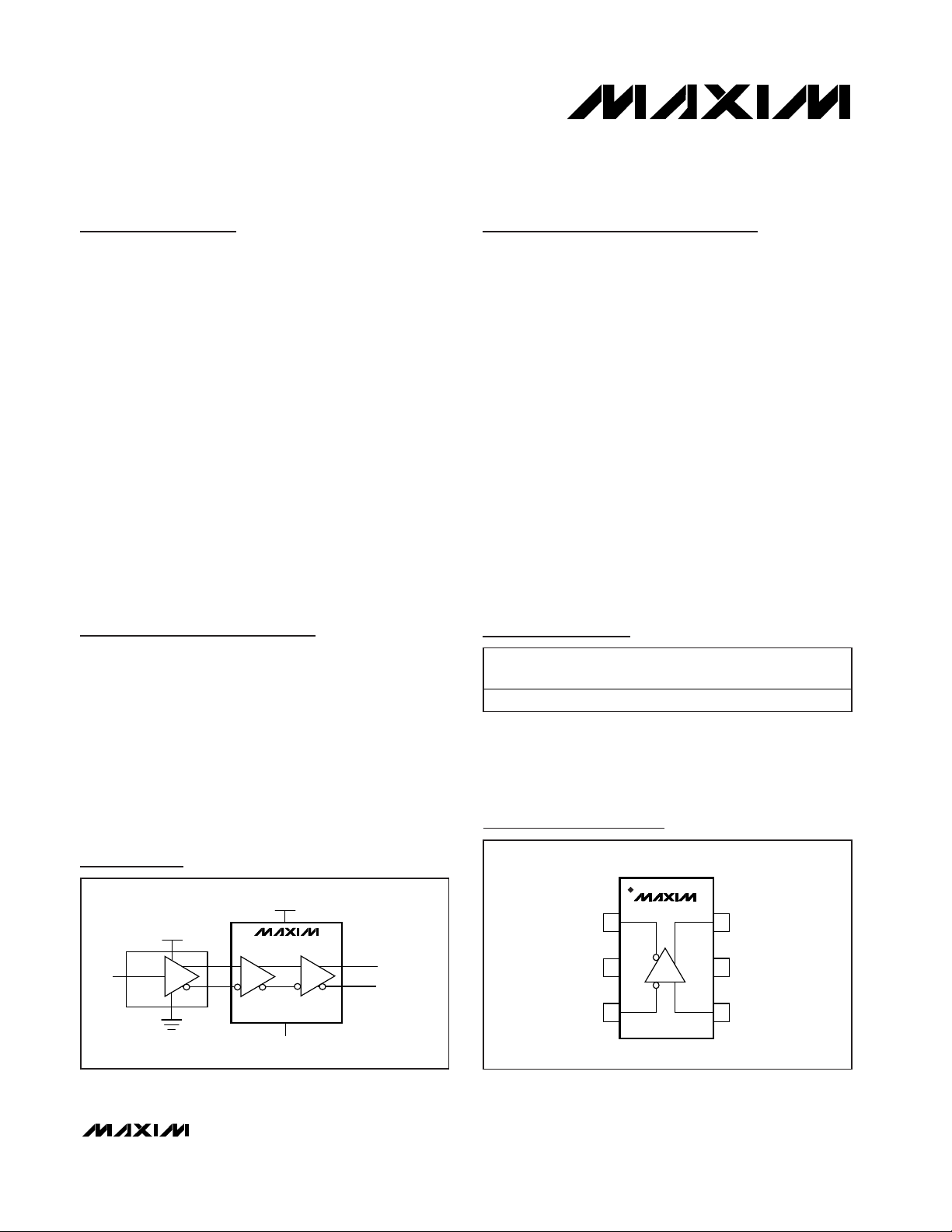
GND
IN+IN-
16OUT+
5V
CC
OUT-
MAX9181
SC70
TOP VIEW
2
34
Pin Configuration
19-2415; Rev 1; 2/04
For pricing, delivery, and ordering information, please contact Maxim/Dallas Direct! at
1-888-629-4642, or visit Maxim’s website at www.maxim-ic.com.
Ordering Information
PART
TEMP RANGE
PIN -
TOP
M ARK
MAX9181EXT-T
6 SC70-6 ABI
Typical Operating Circuit
PA C K A G E
-40°C to +85°C
3.3V
LVPECL
DRIVER
IN+
IN-
MAX9181
V
GND
CC
OUT+
LVDS
OUT-
SIGNALS
MAX9181
Low-Jitter, Low-Noise LVPECL-to-LVDS Level
Translator in an SC70 Package
2 _______________________________________________________________________________________
ABSOLUTE MAXIMUM RATINGS
Stresses beyond those listed under “Absolute Maximum Ratings” may cause permanent damage to the device. These are stress ratings only, and functional
operation of the device at these or any other conditions beyond those indicated in the operational sections of the specifications is not implied. Exposure to
absolute maximum rating conditions for extended periods may affect device reliability.
VCCto GND...........................................................-0.3V to +4.0V
IN+, IN- to GND.....................................................-0.3V to +4.0V
OUT+, OUT- to GND .............................................-0.3V to +4.0V
Short-Circuit Duration (OUT+, OUT-).........................Continuous
Continuous Power Dissipation (T
A
= +70°C)
6-Pin SC70 (derate 3.1mW/°C above +70°C)..............245mW
Operating Temperature Range ...........................-40°C to +85°C
Storage Temperature Range .............................-65°C to +150°C
Junction Temperature......................................................+150°C
ESD Protection
Human Body Model, IN+, IN-, OUT+, OUT-....................±8kV
Lead Temperature (soldering, 10s) .................................+300°C
DC ELECTRICAL CHARACTERISTICS
(VCC= 3.0V to 3.6V, RL= 100Ω ±1%, |V
ID
|
= 0.05V to VCC, VCM= |VID/ 2|to VCC- |VID/ 2|, TA= -40°C to +85°C, unless otherwise
noted. Typical values are at V
CC
= 3.3V, TA= +25°C.) (Notes 1, 2)
PARAMETER
CONDITIONS
U N I T S
LVPECL INPUT
Differential Input High Threshold
V
TH
750mV
Differential Input Low Threshold V
TL
-50 -7 mV
Input Resistor R
IN
Figure 1 360
kΩ
IN+ = 3.6V, IN- = 0V -10
Input Current
IN+ = 0V, IN- = 3.6V -10
µA
IN+ = 3.6V, IN- = 0V -10
Power-Off Input Current
IN+ = 0V, IN- = 3.6V -10
µA
LVDS OUTPUT
Differential Output Voltage V
OD
Figure 2 250
mV
Differential Output Voltage ∆V
OD
Figure 2
25 mV
Offset (Common-Mode) Voltage
V
OS
Figure 2
V
Change in VOS for
Complementary Output States
∆V
OS
Figure 2
25 mV
Output High Voltage V
OH
1.6 V
Output Low Voltage V
OL
0.9
V
Differential Output Voltage V
OD+
IN+, IN- open
mV
-10
Power-Off Output Leakage
Current
O U T- = 3.6V , other outp ut op en -10
µA
Differential Output Resistance
VCC = 3.6V or 0V 100
Ω
VID = 50mV, OUT+ = GND -5 -15
Output Short Current I
SC
VID = -50mV, OUT- = GND -5 -15
mA
POWER SUPPLY
Supply Current I
CC
10 15
mA
SYMBOL
I
, I
IN+
IN-
, I
IN-
VCC = 0V,
Figure 1
I
IN+
MIN TYP MAX
1328
+2.7 +10
+2.7 +10
+2.7 +10
+2.7 +10
IO
OFF
RO
DIFF
VCC = 0V
O U T+ = 3.6V , other outp ut op en
360 450
0.008
1.125 1.25 1.375
+250 +360 +450
0.005
1.44
1.08
+0.02 +10
+0.02 +10
260 400
MAX9181
Low-Jitter, Low-Noise LVPECL-to-LVDS Level
Translator in an SC70 Package
_______________________________________________________________________________________ 3
Note 1: All devices are 100% tested at TA= +25°C. Limits over temperature are guaranteed by design and characterization.
Note 2: Current into a pin is defined as positive. Current out of a pin is defined as negative. All voltages are referenced to ground
except V
TH
, VTL, VOD, and ∆VOD.
Note 3: Guaranteed by design and characterization.
Note 4: Signal generator output (unless otherwise noted): frequency = 200MHz, 50% duty cycle, R
O
= 50Ω, tR= 1.5ns, and tF=
1.5ns (0% to 100%).
Note 5: C
L
includes scope probe and test jig capacitance.
Note 6: Signal generator output for t
DJ
: VOD= 150mV, VOS= 1.2V, tDJincludes pulse (duty cycle) skew.
Note 7: Signal generator output for t
RJ
: VOD= 150mV, VOS= 1.2V.
Note 8: t
SKPP1
is the magnitude difference of any differential propagation delays between devices operating over rated conditions
at the same supply voltage, input common-mode voltage, and ambient temperature.
Note 9: t
SKPP2
is the magnitude difference of any differential propagation delays between devices operating over rated conditions.
Note 10: Device meets V
OD
DC specifications and AC specifications while operating at f
MAX
.
Note 11: Jitter added to the input signal.
AC ELECTRICAL CHARACTERISTICS
(VCC= 3.0V to 3.6V, RL= 100Ω ±1%, CL= 10pF, |V
ID
|
= 0.15V to VCC, VCM= |VID/ 2|to VCC- |VID/ 2|, TA= -40°C to +85°C, unless
otherwise noted. Typical values are at V
CC
= 3.3V, TA= +25°C.) (Notes 3, 4, 5) (Figures 3, 4)
PARAMETER
CONDITIONS
U N I T S
Differential Propagation Delay High
to Low
1.3 2.0 2.8 ns
Differential Propagation Delay Low to
High
1.3 2.0 2.8 ns
Added Deterministic Jitter t
DJ
400Mbps 223 - 1 PRBS data pattern
(Notes 6, 11)
23
ps
P-P
Added Random Jitter t
RJ
fIN = 200MHz (Notes 7, 11) 0.6 2.9
ps
RMS
Differential Part-to-Part Skew
(Note 8)
0.6 ns
Differential Part-to-Part Skew
(Note 9) 1.5 ns
Switching Supply Current
18 mA
Rise Time t
TLH
0.5
1.0 ns
Fall Time t
THL
0.5
1.0 ns
Input Frequency f
MAX
(Note 10) 200
MHz
SYMBOL
MIN TYP MAX
t
PHLD
t
PLHD
t
SKPP1
t
SKPP2
I
CCSW
0.16
12.2
0.67
0.66
100
MAX9181
Low-Jitter, Low-Noise LVPECL-to-LVDS Level
Translator in an SC70 Package
4 _______________________________________________________________________________________
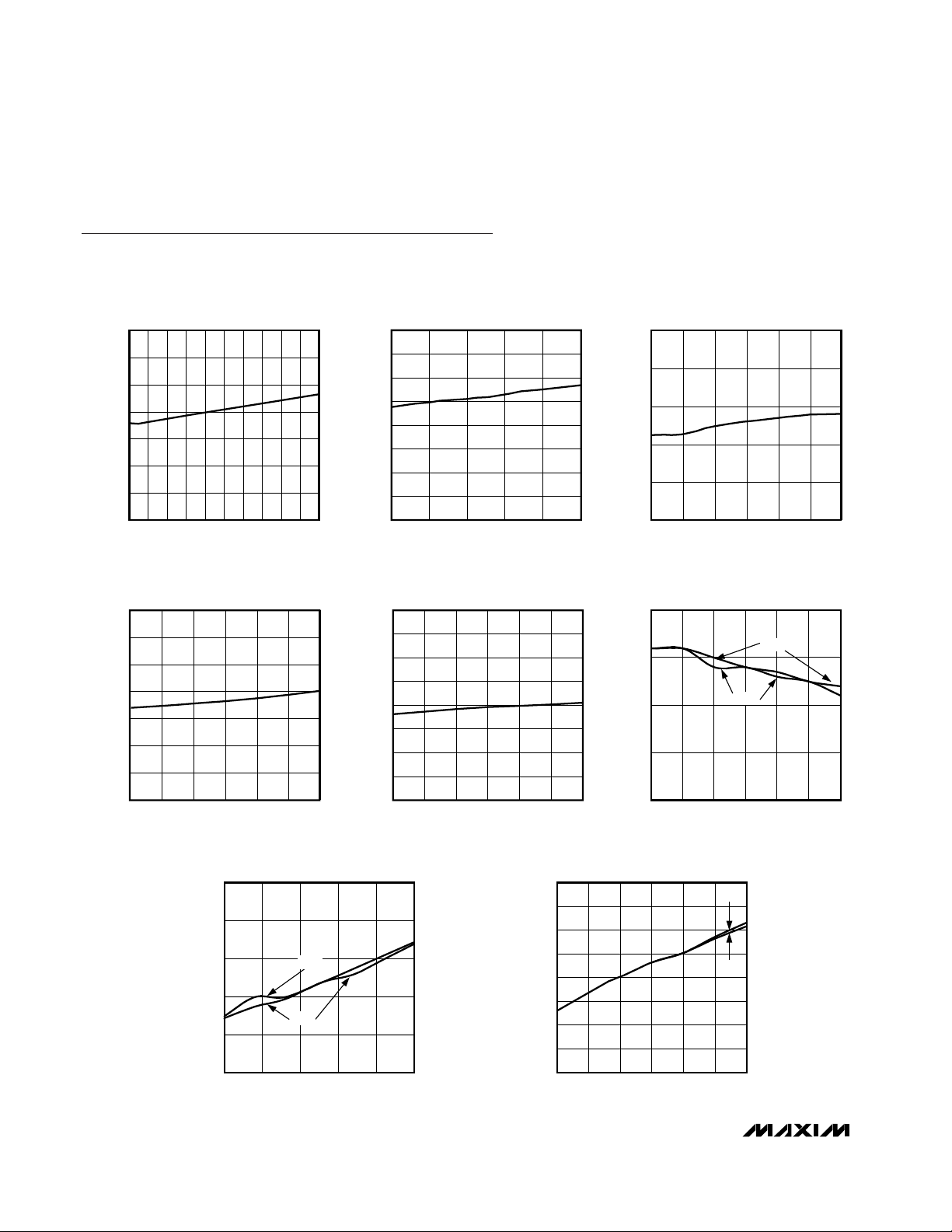
0
6
3
12
9
18
15
0 10050 150 20025 12575 175 225 250
SUPPLY CURRENT
vs. INPUT FREQUENCY
MAX9181 toc01
INPUT FREQUENCY (MHz)
SUPPLY CURRRENT (mA)
21
11.00
11.25
11.50
11.75
12.00
12.25
12.50
12.75
13.00
-40 -15 10 35 60 85
SWITCHING SUPPLY CURRENT
vs. TEMPERATURE
MAX9181 toc02
TEMPERATURE (°C)
SUPPLY CURRENT (mA)
5.05
5.06
5.08
5.07
5.09
5.10
3.0 3.23.1 3.3 3.4 3.5 3.6
OUTPUT SHORT-CIRCUIT CURRENT
vs. SUPPLY VOLTAGE
MAX9181 toc03
SUPPLY VOLTAGE (V)
OUTPUT SHORT-CIRCUIT CURRENT (mA)
1.05
1.07
1.09
1.08
1.10
1.12
3.0 3.23.1 3.3 3.4 3.5 3.6
OUTPUT LOW VOLTAGE
vs. SUPPLY VOLTAGE
MAX9181 toc04
SUPPLY VOLTAGE (V)
OUTPUT LOW VOLTAGE (V)
1.06
1.11
1.350
1.375
1.400
1.425
1.450
1.475
1.500
1.525
1.550
3.0 3.23.1 3.3 3.4 3.5 3.6
OUTPUT HIGH VOLTAGE
vs. SUPPLY VOLTAGE
MAX9181 toc05
SUPPLY VOLTAGE (V)
OUTPUT HIGH VOLTAGE (V)
2.1
2.0
1.9
1.8
1.7
3.0 3.33.1 3.2 3.4 3.5 3.6
DIFFERENTIAL PROPAGATION DELAY
vs. SUPPLY VOLTAGE
MAX9181 toc06
SUPPLY VOLTAGE (V)
DIFFERENTIAL PROPAGATION DELAY (ns)
t
PHLD
t
PLHD
1.5
1.7
2.1
1.9
2.3
2.5
-40 10-15 35 60 85
DIFFERENTIAL PROPAGATION DELAY
vs. TEMPERATURE
MAX9181 toc07
TEMPERATURE (°C)
DIFFERENTIAL PROPAGATION DELAY (ns)
t
PHLD
t
PLHD
550
575
600
625
650
675
700
725
750
3.0 3.23.1 3.3 3.4 3.5 3.6
TRANSITION TIME
vs. SUPPLY VOLTAGE
MAX9181 toc08
SUPPLY VOLTAGE (V)
TRANSITION TIME (ps)
t
THL
t
TLH
Typical Operating Characteristics
(VCC= 3.3V, RL= 100Ω ±1%, CL= 10pF, |V
ID
|
= 0.2V, VCM= 1.2V, TA= +25°C, unless otherwise noted. Signal generator output:
frequency = 200MHz, 50% duty cycle, R
O
= 50Ω, tR= 1.5ns, and tF= 1.5ns (0% to 100%), unless otherwise noted.)

Detailed Description
The LVDS interface standard is a signaling method
intended for point-to-point communication over a controlled-impedance medium, as defined by the ANSI/
TIA/EIA-644 and IEEE 1596.3 standards. The LVDS
standard uses a lower voltage swing than other common communication standards, achieving higher data
rates with reduced power consumption while reducing
EMI emissions and system susceptibility to noise.
The MAX9181 is a 400Mbps LVDS translator intended
for high-speed, point-to-point, low-power applications.
The MAX9181 accepts differential LVPECL inputs and
produces an LVDS output. The input voltage range
includes signals from GND up to VCC, allowing interoperation with 3.3V LVPECL devices.
The MAX9181 provides a high output when the inputs
are open. See Table 1.
MAX9181
Low-Jitter, Low-Noise LVPECL-to-LVDS Level
Translator in an SC70 Package
_______________________________________________________________________________________ 5
400
450
500
550
600
650
700
750
800
-40 -15 10 35 60 85
TRANSITION TIME
vs. TEMPERATURE
MAX9181 toc09
TEMPERATURE (°C)
TRANSITION TIME (ps)
t
TLH
, t
THL
0
200
100
400
300
500
600
25 150
DIFFERENTIAL OUTPUT VOLTAGE
vs. LOAD RESISTOR
MAX9181 toc10
LOAD RESISTOR (Ω)
DIFFERENTIAL OUTPUT VOLTAGE (mV)
7550 100 125
Typical Operating Characteristics (continued)
(VCC= 3.3V, RL= 100Ω ±1%, CL= 10pF, |V
ID
|
= 0.2V, VCM= 1.2V, TA= +25°C, unless otherwise noted. Signal generator output:
frequency = 200MHz, 50% duty cycle, R
O
= 50Ω, tR= 1.5ns, and tF= 1.5ns (0% to 100%), unless otherwise noted.)
Pin Description
PIN
NAME FUNCTION
1 OUT- Inverting LVDS Output
2 GND Ground
3 IN- Inverting LVPECL-Compatible Input
4 IN+
Noninverting LVPECL-Compatible
Input
5V
CC
Power Supply. Bypass VCC to GND
with a 0.01µF ceramic capacitor.
6 OUT+ Noninverting LVDS Output
Note: VID= (IN+ - IN-), VOD= (OUT+ - OUT-)
High = 450mV ≥ V
OD
≥ 250mV
Low = -250mV ≥ V
OD
≥ -450mV
Table 1. Function Table (Figure 2)
INPUT, V
50mV > VID > -50mV Indeterminate
ID
> 50mV High
< -50mV Low
Open High
OUTPUT, V
OD

MAX9181
Applications Information
Supply Bypassing
Bypass VCCwith a high-frequency surface-mount
ceramic 0.01µF capacitor as close to the device as
possible.
Differential Traces
Input and output trace characteristics affect the performance of the MAX9181. Use controlled-impedance differential traces. Ensure that noise couples as common
mode by running the traces within a differential pair
close together.
Maintain the distance within a differential pair to avoid
discontinuities in differential impedance. Avoid 90°
turns and minimize the number of vias to further prevent
impedance discontinuities.
Cables and Connectors
The LVDS standards define signal levels for interconnect with a differential characteristic impedance and
termination of 100Ω. Interconnects with a characteristic
impedance and termination of 90Ω to 132Ω impedance
are allowed, but produce different signal levels (see
Termination).
LVPECL signals are typically specified for 50Ω single-
ended characteristic impedance interconnect terminated through 50Ω to VCC- 2V.
Use cables and connectors that have matched differential impedance to minimize impedance discontinuities.
Termination
For point-to-point LVDS links, the termination resistor
should be located at the LVDS receiver input and
match the differential characteristic impedance of the
transmission line.
Each line of a differential LVPECL link should be terminated through 50Ω to VCC- 2V or be replaced by the
Thevinin equivalent.
The LVDS output voltage level depends upon the differential characteristic impedance of the interconnect and
the value of the termination resistance. The MAX9181 is
guaranteed to produce LVDS output levels into 100Ω.
With the typical 3.6mA output current, the MAX9181 produces an output voltage of 360mV when driving a 100Ω
transmission line terminated with a 100Ω termination
resistor (3.6mA ✕100Ω = 360mV). For typical output levels with different loads, see the Differential Output
Voltage vs. Load Resistor curve in the Typical Operating
Characterics.
Chip Information
TRANSISTOR COUNT: 401
PROCESS: CMOS
Low-Jitter, Low-Noise LVPECL-to-LVDS Level
Translator in an SC70 Package
6 _______________________________________________________________________________________
MAX9181
Low-Jitter, Low-Noise LVPECL-to-LVDS Level
Translator in an SC70 Package
_______________________________________________________________________________________ 7
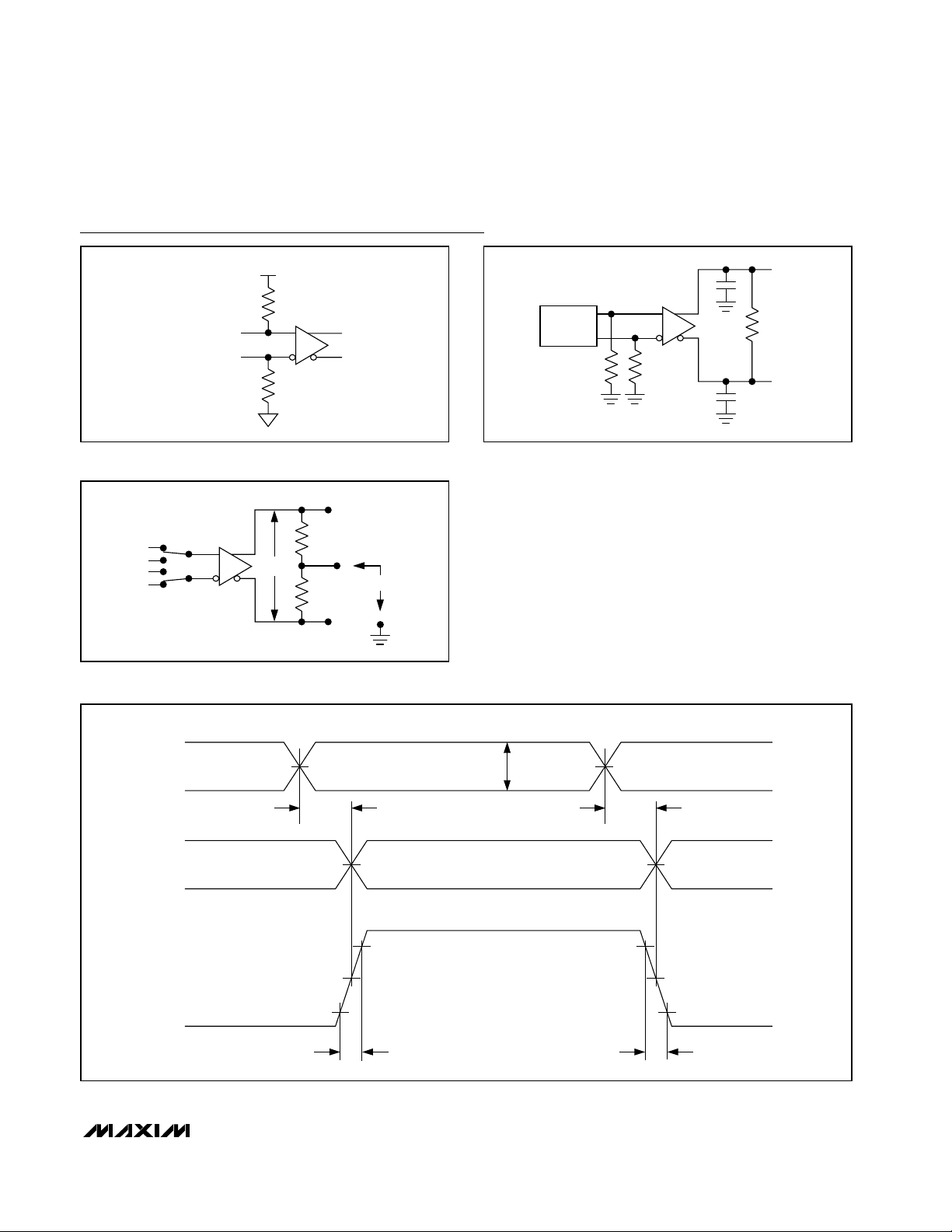
Figure 2. DC Load Test Circuit
V
OD
1.25V
IN+
IN-
1.20V
1.25V
1.20V
R
L
/2
R
L
/2
OUT-
OUT+
V
OS
Figure 3. Transition Time and Propagation Delay Test Circuit
C
L
PULSE
GENERATOR
IN+
IN-
R
L
50Ω50Ω
OUT-
OUT+
C
L
Test Circuits and Timing Diagrams
Figure 1. LVPECL Input Bias
R
IN
R
IN
OUT-
OUT+
V
CC
IN+
IN-
Figure 4. Transition Time and Propagation Delay Timing Diagram
IN-
V
CM
= ((IN+) + (IN-))/2
V
DIFF
= (OUT+) - (OUT-)
IN+
OUT-
OUT+
t
PLHD
t
TLH
t
THL
t
PHLD
OV (DIFFERENTIAL)
OV (DIFFERENTIAL)
OV (DIFFERENTIAL)
80% 80%
20% 20%
OV (DIFFERENTIAL)
OV (DIFFERENTIAL)
OV (DIFFERENTIAL)
V
DIFF
V
ID

MAX9181
Low-Jitter, Low-Noise LVPECL-to-LVDS Level
Translator in an SC70 Package
Maxim cannot assume responsibility for use of any circuitry other than circuitry entirely embodied in a Maxim product. No circuit patent licenses are
implied. Maxim reserves the right to change the circuitry and specifications without notice at any time.
8 _____________________Maxim Integrated Products, 120 San Gabriel Drive, Sunnyvale, CA 94086 408-737-7600
© 2004 Maxim Integrated Products Printed USA is a registered trademark of Maxim Integrated Products.
SC70, 6L.EPS
Package Information
(The package drawing(s) in this data sheet may not reflect the most current specifications. For the latest package outline information,
go to www.maxim-ic.com/packages.)
 Loading...