

Page 1
General Description
The MAX9179 is a quad low-voltage differential
signaling (LVDS) line receiver designed for applications
requiring high data rates, low power dissipation, and
noise immunity. The receiver accepts four LVDS input
signals and translates them to 3.3V LVCMOS output levels at speeds up to 400Mbps. The receiver features
built-in hysteresis, which improves noise immunity and
prevents multiple switching on slow transitioning inputs.
The device supports a wide 0.038V to 2.362V commonmode input voltage range, allowing for ground potential
differences and common-mode noise between the driver
and the receiver. A fail-safe circuit sets the output high
when the input is open, undriven and shorted, or undriven
and terminated. Common enable inputs control the highimpedance outputs.
The MAX9179 has a flow-through pinout for easy PC
board layout, and is pin compatible with the MAX9121
and the DS90LV048A with the additional features of
high ESD tolerance and built-in hysteresis.
The MAX9179 operates from a single 3.3V supply, and is
specified for operation from -40°C to +85°C. The device
is offered in 16-pin TSSOP and thin QFN packages.
Applications
Laser Printers
Digital Copiers
Cell-Phone Base Stations
Telecom Switching Equipment
LCD Displays
Network Switches/Routers
Backplane Interconnect
Clock Distribution
Features
♦ Guaranteed 400Mbps Data Rate
♦ 50mV (typ) Hysteresis
♦ Overshoot/Undershoot Protection (-1.0V or V
CC
+
1.0V) on Enables
♦ IEC61000-4-2 Level 4 ESD Tolerance
♦ AC Specifications Guaranteed with |V
ID|=
100mV
♦ Single 3.3V Supply
♦ Fail-Safe Circuit
♦ Flow-Through Pinout
Simplifies PC Board Layout
Reduces Crosstalk
♦ Low-Power CMOS Design
♦ Conforms to ANSI TIA/EIA-644 LVDS Standard
♦ High-Impedance Inputs when Powered Off
♦ Pin Compatible with the MAX9121 and the
DS90LV048A
♦ Small Thin QFN Package Available
MAX9179
Quad LVDS Receiver with Hysteresis
________________________________________________________________ Maxim Integrated Products 1
Ordering Information
19-2752; Rev 0; 2/03
For pricing, delivery, and ordering information, please contact Maxim/Dallas Direct! at
1-888-629-4642, or visit Maxim’s website at www.maxim-ic.com.
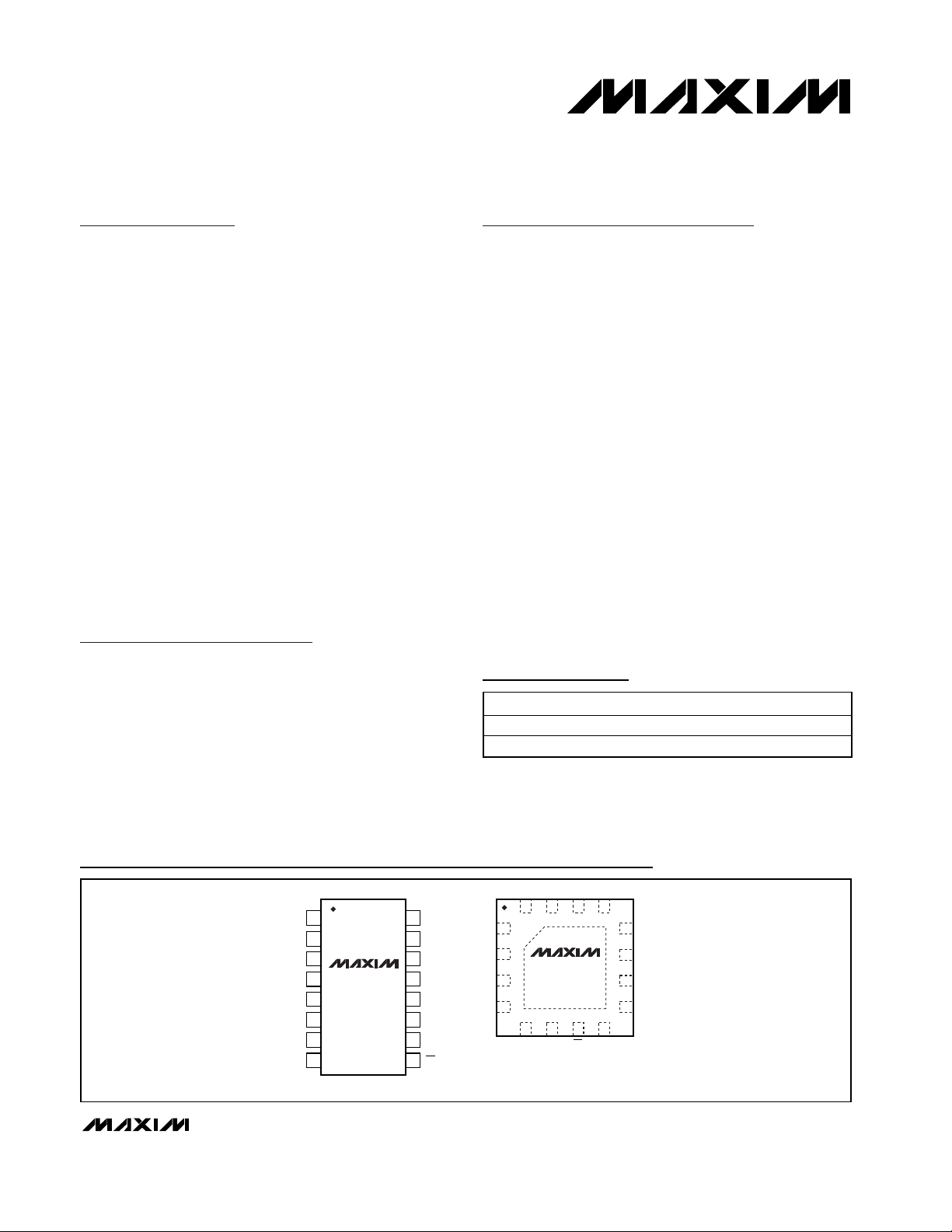
Pin Configurations
Functional Diagram appears at end of data sheet.
*Future product—contact factory for availability.
**EP = Exposed paddle.
PART TEMP RANGE PIN-PACKAGE
MAX9179EUE -40°C to +85°C 16 TSSOP
MAX9179ETE* -40°C to +85°C 16 Thin QFN-EP**
TOP VIEW
IN1-
IN1+
IN2+
IN2-
IN3-
IN3+
IN4+
IN4-
EN
1
2
3
MAX9179
4
5
6
7
8
TSSOP
16
OUT1
15
OUT2
14
V
13
CC
12
GND
OUT3
11
10
OUT4
EN
9
16 15 14 13
IN2+
1
2
IN2-
IN3-
IN3+
(LEADS UNDER PACKAGE)
MAX9179
3
EXPOSED PAD
4
5678
THIN QFN
OUT1IN1-IN1+ EN
OUT4IN4-IN4+
EN
12
OUT2
11
V
CC
10
GND
9
OUT3
Page 2

MAX9179
Quad LVDS Receiver with Hysteresis
2 _______________________________________________________________________________________
ABSOLUTE MAXIMUM RATINGS
DC ELECTRICAL CHARACTERISTICS
(VCC= 3.0V to 3.6V, differential input voltage |VID| = 0.075V to 1.2V, input common-mode voltage VCM= |VID/2| to 2.4V - |VID/2|,
T
A
= -40°C to +85°C, unless otherwise noted. Typical values are at VCC= 3.3V, |VID| = 0.2V, VCM= 1.2V, TA= +25°C.) (Notes 1, 2)
Stresses beyond those listed under “Absolute Maximum Ratings” may cause permanent damage to the device. These are stress ratings only, and functional
operation of the device at these or any other conditions beyond those indicated in the operational sections of the specifications is not implied. Exposure to
absolute maximum rating conditions for extended periods may affect device reliability.
VCCto GND...........................................................-0.3V to +4.0V
IN_+, IN_- to GND .................................................-0.3V to +4.0V
EN, EN to GND...........................................-1.4V to (V
CC
+ 1.4V)
OUT_ to GND .............................................-0.3V to (V
CC
+ 0.3V)
Continuous Power Dissipation (T
A
= +70°C)
16-Pin TSSOP (derate 9.4mW/°C above +70°C) .........755mW
16-Pin Thin QFN (derate 16.9mW/°C
above +70°C).............................................................1349mW
Junction Temperature......................................................+150°C
Storage Temperature Range .............................-65°C to +150°C
ESD Protection
Human Body Model (R
D
= 1.5kΩ, CS= 100pF)
(IN_+, IN_-) ................................................................±16kV
IEC61000-4-2 (R
D
= 330Ω, CS= 150pF) (IN_+, IN_-)
Contact Discharge .......................................................±8kV
Air-Gap Discharge .....................................................±15kV
Soldering Temperature (soldering, 10s) ..........................+300°C
INPUTS (IN_+, IN_-)
Differential Input High Threshold V
Differential Input Low Threshold V
Hysteresis V
Input Current I
Power-Off Input Current
Fail-Safe Input Resistor 1 R
Fail-Safe Input Resistor 2 R
OUTPUTS (OUT_)
Output High Voltage V
Output Low Voltage V
Output Short-Circuit Current I
Output High-Impedance Current I
ENABLE INPUTS (EN, EN)
Input High Voltage V
Input Low Voltage V
POWER SUPPLY
Supply Current I
Disabled Supply Current I
PARAMETER SYMBOL CONDITIONS MIN TYP MAX UNITS
Figure 1 25 75 mV
TH
Figure 1 -75 -25 mV
TL
- VTLFigure 1 50 mV
TH
IN+, IIN-
I
OFF+,
I
OFF-
IN1
IN2
OH
OS
OZ
OL
IH
IL
V
= 0V -20 +20 µA
CC
V
= 3.6V or 0V, Figure 2 40 65 kΩ
CC
V
= 3.6V or 0V, Figure 2 280 455 kΩ
CC
IOH = -4.0mA
IOL = 4.0mA, V
Enabled, V
Disabled, V
ID
OUT
-1.0V ≤ EN, EN ≤ 0V -1800 +10
IN
0V ≤ EN, EN ≤ V
VCC ≤ EN, EN ≤ VCC + 1.0V -10 +1800
CC
CCZ
Enabled, inputs open 10.4 15
Disabled, inputs open 0.6 1.0
-20 +20 µA
Open, undriven short, or
undriven parallel
termination
= +50mV
V
ID
= -50mV 0.1 0.25 V
ID
= +50mV, V
= 0 or V
= 0 (Note 3) -40 -70 -120 mA
OUT
CC
V
-
VCC -
CC
0.2
0.1
-1.0 +1.0 µA
V
2.0
CC
1.0
-1.0 +0.8 V
CC
-20 +20Input Current I
+
V
V
µA
mA
Page 3
MAX9179
Quad LVDS Receiver with Hysteresis
_______________________________________________________________________________________ 3
Note 1: Maximum and minimum limits over temperature are guaranteed by design and characterization. Parts are production
tested at T
A
= +25°C.
Note 2: Current into a pin is defined as positive. Current out of a pin is defined as negative. All voltages are referenced to ground
except V
TH
, VTL, and VID.
Note 3: Short one output at a time.
Note 4: AC parameters are guaranteed by design and characterization. Limits are set at ±6 sigma.
Note 5: C
L
includes scope probe and test jig capacitance.
Note 6: Pulse generator differential output for all tests (unless otherwise noted): t
R
= tF< 1ns (0% to 100%), frequency = 100MHz,
50% duty cycle.
Note 7: t
SKD1
is the magnitude of the difference of the differential propagation delays in a channel. t
SKD1
= | t
PHLD
- t
PLHD
|.
Note 8: t
SKD2
is the magnitude of the difference of the t
PLHD
or t
PHLD
of one channel and the t
PLHD
or t
PHLD
of the other channel
on the same part.
Note 9: t
SKD3
is the magnitude of the difference of any differential propagation delays between parts at the same VCCand within
5°C of each other.
Note 10: t
S
KD4
is the magnitude of the difference of any differential propagation delays between parts operating over the rated
supply and temperature ranges.
Note 11: Pulse generator output for t
PHZ
, t
PLZ
, t
PZH
, and t
PZL
tests: tR= tF= 1.5ns (0.2VCCto 0.8VCC), 50% duty cycle, VOH=
V
CC
+ 1.0V settling to VCC, VOL= -1.0V settling to 0, frequency = 1MHz.
AC ELECTRICAL CHARACTERISTICS
(VCC= 3.0V to 3.6V, CL= 15pF, differential input voltage |VID| = 0.1V to 1.2V, input common-mode voltage VCM= |VID/2| to 2.4V - |VID/2|,
T
A
= -40°C to +85°C, unless otherwise noted. Typical values are at VCC= 3.3V, |VID| = 0.2V, VCM= 1.2V, TA= +25°C.) (Notes 4, 5, 6)
Differential Propagation Delay
High to Low
Differential Propagation Delay
Low to High
Differential Pulse Skew
| t
PHLD
Differential Channel-to-Channel
Skew, Same Part
(Note 8)
Differential Part-to-Part Skew
(Note 9)
Differential Part-to-Part Skew
(Note 10)
Rise Time t
Fall Time t
Disable Time High to Z
Disable Time Low to Z t
Enable Time Z to High t
Enable Time Z to Low t
Maximum Operating Frequency f
PARAMETER SYMBOL CONDITIONS MIN TYP MAX UNITS
t
PHLD
t
PLHD
Figures 3, 4 2.0 2.6 4.6 ns
Figures 3, 4 2.0 2.52 4.6 ns
|VID| = 0.1V to 0.15V 700
- t
PLHD
| (Note 7)
t
SKD1
|VID| = 0.15V to 0.2V 400
|VID| = 0.2V to 1.2V 80 300
|VID| = 0.1V to 0.15V 900
t
SKD2
|VID| = 0.15V to 0.2V 600
|VID| = 0.2V to 1.2V 120 400
t
SKD3
t
SKD4
TLH
THL
t
PHZ
PLZ
PZH
PZL
MAX
0.77 1.4 ns
0.74 1.4 ns
RL = 2kΩ, Figures 5, 6 (Note 11) 10.6 14 ns
RL = 2kΩ, Figures 5, 6 (Note 11) 11 14 ns
RL = 2kΩ, Figures 5, 6 (Note 11) 4.8 14 ns
RL = 2kΩ, Figures 5, 6 (Note 11) 4.8 14 ns
All channels switching, CL = 15pF, V
(max) = 0.25V, VOH (min) = VCC - 0.2V,
OL
200 250 MHz
2.0 ns
2.6 ns
44% < duty cycle < 56%
ps
ps
Page 4
MAX9179
Quad LVDS Receiver with Hysteresis
4 _______________________________________________________________________________________
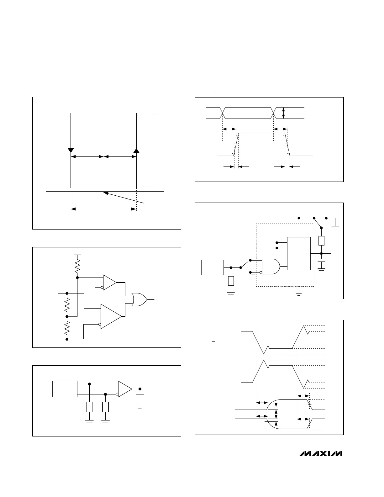
Test Circuits/Timing Diagrams
Figure 1. Input Thresholds and Hysteresis
Figure 2. Fail-Safe Input Circuit
Figure 3. Propagation Delay and Transition Time Test Circuit
Figure 4. Propagation Delay and Transition Time Waveforms
Figure 5. High-Impedance Delay Test Circuit
Figure 6. High-Impedance Delay Waveforms
IN_-
IN_+
OUT_
(0V DIFFERENTIAL) V
t
PLHD
0.9V
CC
0.5V
CC
0.1V
CC
V
OUT
V
TL
V
TH
V
OH
t
PHLD
VCM = ((V
) + (V
ID
0.9V
CC
0.5V
CC
0.1V
CC
))/2
IN_+
IN_-
-V
ID
HYSTERESIS
V
CC
R
IN2
IN_+
R
IN1
R
IN1
VCC - 0.3V
IN_-
PULSE
GENERATOR
IN_+
IN_-
50Ω50Ω
t
TLH
V
OL
+V
ID
= 0
V
ID
INCLUDES LOAD AND TEST JIG CAPACITANCE.
C
L
= VCC FOR t
S
1
= 0 FOR t
S
1
PZH
PZL
AND t
AND t
MEASUREMENTS.
PLZ
MEASUREMENTS.
PHZ
EN
PULSE
GENERATOR
50Ω
EN
IN_+
IN_-
t
THL
V
CC
DEVICE
UNDER
TEST
S
1
R
L
OUT_
C
L
OUT_
VCC + 1.0V
V
CC
EN WHEN EN = LOW OR OPEN
EN WHEN EN = HIGH
OUT_
C
L
OUT_ WHEN VID = -75mV
OUT_ WHEN V
= +75mV
ID
1.5V 1.5V
1.5V 1.5V
t
PLZ
t
PHZ
0.5V
0.5V
0
-1.0V
V
+ 1.0V
CC
V
CC
0
50%
50%
V
V
V
0
-1.0V
CC
OL
OH
t
PZL
t
PZH
Page 5

Typical Operating Characteristics
(VCC= 3.3V, VCM= 1.2V, |VID| = 0.15V, CL= 15pF, f = 100MHz, TA= +25°C, unless otherwise noted.)
MAX9179
Quad LVDS Receiver with Hysteresis
_______________________________________________________________________________________ 5
SUPPLY CURRENT vs. FREQUENCY
110
90
70
50
SUPPLY CURRENT (mA)
30
10
0 350
ALL CHANNELS DRIVEN
FREQUENCY (MHz)
OUTPUT SHORT-CIRCUIT CURRENT
vs. SUPPLY VOLTAGE
-100
DC INPUT
= +150mV)
(V
ID
-80
-60
SUPPLY CURRENT
vs. TEMPERATURE
16
14
MAX9179 toc01
12
10
8
SUPPLY CURRENT (mA)
6
30025020015010050
4
-40 85
TEMPERATURE (°C)
MAX9179 toc04
INPUTS OPEN
603510-15
3.6
3.4
3.2
3.0
MAX9179 toc02
DC INPUT
= +150mV)
(V
ID
= -4mA
I
OH
DC DIFFERENTIAL THRESHOLD VOLTAGE
40
30
20
10
0
-10
-20
-30
DC DIFFERENTIAL THRESHOLD VOLTAGE (mV)
-40
3.0 3.6
OUTPUT HIGH VOLTAGE
vs. SUPPLY VOLTAGE
vs. SUPPLY VOLTAGE
V
TH
V
TL
SUPPLY VOLTAGE (V)
MAX9179 toc05
MAX9179 toc03
3.53.43.1 3.2 3.3
-40
OUTPUT SHORT-CIRCUIT CURRENT (mA)
-20
3.0 3.6
SUPPLY VOLTAGE (V)
OUTPUT LOW VOLTAGE
vs. SUPPLY VOLTAGE
140
DC INPUT
= -150mV)
(V
ID
= 4mA
I
OL
130
120
110
OUTPUT LOW VOLTAGE (mV)
100
90
3.0 3.6
SUPPLY VOLTAGE (V)
3.53.43.33.23.1
MAX9179 toc06
3.53.43.33.23.1
OUTPUT HIGH VOLTAGE (V)
2.8
2.6
3.0 3.6
SUPPLY VOLTAGE (V)
DIFFERENTIAL PROPAGATION DELAY
vs. SUPPLY VOLTAGE
3.2
3.0
2.8
t
2.6
2.4
2.2
DIFFERENTIAL PROPAGATION DELAY (ns)
2.0
3.0 3.6
PHLD
t
PLHD
SUPPLY VOLTAGE (V)
3.53.43.33.23.1
MAX9179 toc07
3.53.43.33.23.1
Page 6

Typical Operating Characteristics (continued)
(VCC= 3.3V, VCM= 1.2V, |VID| = 0.15V, CL= 15pF, f = 100MHz, TA= +25°C, unless otherwise noted.)
MAX9179
Quad LVDS Receiver with Hysteresis
6 _______________________________________________________________________________________
DIFFERENTIAL PROPAGATION DELAY
vs. TEMPERATURE
3.4
3.2
3.0
2.8
2.6
2.4
2.2
DIFFERENTIAL PROPAGATION DELAY (ns)
2.0
-40 85
TEMPERATURE (°C)
200
150
100
50
DIFFERENTIAL PULSE SKEW (ps)
-50
t
PHLD
t
PLHD
603510-15
DIFFERENTIAL PULSE SKEW
vs. SUPPLY VOLTAGE
0
DIFFERENTIAL PROPAGATION DELAY
vs. COMMON-MODE VOLTAGE
3.4
3.2
MAX9179 toc08
3.0
t
PLHD
2.8
t
PHLD
2.6
2.4
2.2
2.0
DIFFERENTIAL PROPAGATION DELAY (ns)
1.8
0.075 2.325
COMMON-MODE VOLTAGE (V)
MAX9179 toc11
MAX9179 toc09
1.8751.4250.525 0.975
1100
1000
900
t
TLH
800
700
TRANSITION TIME (ps)
t
THL
600
DIFFERENTIAL PROPAGATION DELAY
vs. DIFFERENTIAL INPUT VOLTAGE
3.0
2.8
t
2.6
2.4
2.2
2.0
DIFFERENTIAL PROPAGATION DELAY (ns)
1.8
0.10 1.20
PHLD
t
PLHD
DIFFERENTIAL INPUT VOLTAGE (V)
TRANSITION TIME
vs. SUPPLY VOLTAGE
MAX9179 toc12
MAX9179 toc10
0.930.650.38
-100
3.0 3.6
SUPPLY VOLTAGE (V)
3.53.43.33.23.1
500
3.0 3.6
SUPPLY VOLTAGE (V)
3.53.43.33.23.1
DIFFERENTIAL THRESHOLD VOLTAGE
TRANSITION TIME vs. TEMPERATURE
1200
1100
1000
900
800
700
TRANSITION TIME (ps)
600
500
400
-40 85
t
TLH
t
THL
TEMPERATURE (°C)
MAX9179 toc13
DIFFERENTIAL THRESHOLD VOLTAGE (mV)
603510-15
vs. COMMON-MODE VOLTAGE
40
30
20
10
0
-10
-20
-30
-40
0.075 2.325
V
TH
V
TL
COMMON-MODE VOLTAGE (V)
1.8751.4250.9750.525
MAX9179 toc14
Page 7

MAX9179
Quad LVDS Receiver with Hysteresis
__________________________________________________________________________
Pin Description
PIN
TSSOP QFN
1 15 IN1- Inverting LVDS Input 1
2 16 IN1+ Noninverting LVDS Input 1
3 1 IN2+ Noninverting LVDS Input 2
4 2 IN2- Inverting LVDS Input 2
5 3 IN3- Inverting LVDS Input 3
6 4 IN3+ Noninverting LVDS Input 3
7 5 IN4+ Noninverting LVDS Input 4
8 6 IN4- Inverting LVDS Input 4
97EN
10 8 OUT4 LVCMOS/LVTTL Output 4
11 9 OUT3 LVCMOS/LVTTL Output 3
12 10 GND Ground
13 11 V
14 12 OUT2 LVCMOS/LVTTL Output 2
15 13 OUT1 LVCMOS/LVTTL Output 1
16 14 EN
— EP
NAME FUNCTION
Enable Complementary Input. The outputs are active when EN = high and EN = low or open. For
all other combinations of EN and EN, the outputs are disabled and in high impedance.
Power-Supply Input. Bypass VCC to GND with 0.1µF and 0.001µF ceramic capacitors.
CC
Enable Input. The outputs are active when EN = high and EN = low or open. For all other
combinations of EN and EN, the outputs are disabled and in high impedance.
Exposed
Pad
Exposed Pad. Connect to ground.
Page 8

MAX9179
Quad LVDS Receiver with Hysteresis
8 _______________________________________________________________________________________
Detailed Description
The LVDS is a signaling method intended for point-topoint communication over a controlled-impedance
medium as defined by the ANSI TIA/EIA-644 and IEEE
1596.3 standards.
The MAX9179 is a quad LVDS line receiver with built-in
hysteresis, intended for high-speed, point-to-point, lowpower applications. The receiver accepts four LVDS
input signals and translates them to 3.3V LVCMOS output levels at speeds up to 400Mbps over controlledimpedance media of 100Ω. The hysteresis improves
noise immunity and prevents multiple switching due to
noise on slow input transitions at the end of a long cable.
The receiver is capable of detecting differential signals
as low as 75mV and as high as 1.2V within a 0 to 2.4V
input voltage range. The 250mV to 450mV differential
output of an LVDS driver is nominally centered on a 1.2V
offset. This offset, coupled with the receiver’s 0 to 2.4V
input voltage range, allows an approximate ±1V shift in
the signal (as seen by the receiver). This allows for a difference in ground references of the transmitter and the
receiver, the common-mode effects of coupled noise, or
both. The LVDS standards specify an input voltage
range of 0 to 2.4V referenced to receiver ground.
Hysteresis
The MAX9179 incorporates hysteresis of 50mV (typ),
which rejects noise and prevents false switching during
low-slew-rate transitions at the end of a long cable. The
receiver typically switches at 25mV above or below V
ID
= 0V (Figure 1). The hysteresis is designed to be symmetrical around VID= 0V for low pulse distortion (see
the Typical Operating Characteristics).
Input Fail-Safe
The fail-safe feature of the MAX9179 sets the output
high when the differential input is:
• Open
• Undriven and shorted
• Undriven and terminated
Without a fail-safe circuit, when the input is undriven,
noise at the input may switch the output and it may
appear to the system that data is being sent. Open or
undriven terminated input conditions can occur when a
cable is disconnected or cut, or when a driver output is
in high impedance. A shorted input can occur because
of a cable failure.
When the input is driven with a differential signal of |V
ID
|
= 75mV to 1.2V within a voltage range of 0 to 2.4V, the
fail-safe circuit is not activated. If the input is open,
undriven and shorted, or undriven and terminated, an
internal resistor in the fail-safe circuit pulls both inputs
above VCC- 0.3V, activating the fail-safe circuit and
forcing the output high (Figure 2).
Overshoot and Undershoot
Voltage Protection
The MAX9179 is designed to protect the enable inputs
(EN and EN) against latchup due to transient overshoot
and undershoot voltage. If the enable input voltage
goes above VCCor below GND by up to 1V, an internal
circuit clamps and limits input current to 1.8mA.
Applications Information
Power-Supply Bypassing
Bypass the VCCpin with high-frequency surface-mount
ceramic 0.1µF and 0.001µF capacitors in parallel as
close to the device as possible, with the smaller valued
capacitor closest to VCC.
Differential Traces
Input trace characteristics affect the performance of the
MAX9179. Use controlled-impedance differential traces
(100Ω is typical). To reduce radiated noise and ensure
that noise couples as common mode, route the differential input signals within a pair close together. Reduce
skew by matching the electrical length of the signal
paths making up the differential pair. Excessive skew
can result in a degradation of magnetic field cancellation. Maintain a constant distance between the differential traces to avoid discontinuities in differential
impedance. Minimize the number of vias to further prevent impedance discontinuities.
H = High logic level
L = Low logic level
X = Don't care
Z = High impedance
Table 1. Functional Table
ENABLES INPUTS OUTPUT
EN EN (IN_+) - (IN_-) OUT_
≥ +75mV H
H L or open
All other combinations
of enable inputs
≤ -75mV L
Open, undriven short,
or undriven terminated
XZ
H
Page 9

MAX9179
Quad LVDS Receiver with Hysteresis
_______________________________________________________________________________________ 9
Cables and Connectors
Interconnect for LVDS typically has a controlled differential impedance of 100Ω. Use cables and connectors
that have matched differential impedance to minimize
impedance discontinuities. Avoid the use of unbalanced cables such as ribbon or simple coaxial cable.
Balanced cables such as twisted pair offer superior
signal quality and tend to generate less EMI due to
magnetic field canceling effects. Balanced cables pick
up noise as common mode, which is rejected by the
LVDS receiver.
Termination
The MAX9179 requires external termination resistors.
The input termination resistor used on each active
channel should match the differential impedance of the
transmission line. Place the termination resistor as
close to the MAX9179 receiver input as possible. Use
1% surface-mount resistors.
Board Layout
Keep the LVDS input and LVCMOS output signals separated from each other to reduce crosstalk; 180 degrees of
separation between LVDS inputs and LVCMOS outputs is
recommended. Because there are leads on all sides, this
separation requires special attention when laying out
traces for the QFN package.
A four-layer printed circuit board with separate layers
for power, ground, LVDS inputs, and single-ended
logic signals is recommended. Separate the LVDS signals from the single-ended signals with power and
ground planes for best results.
IEC 61000-4-2 Level 4 ESD Protection
The IEC 61000-4-2 standard (Figure 7) specifies ESD
tolerance for electronic systems. The IEC61000-4-2
model specifies a 150pF capacitor that is discharged
into the device through a 330Ω resistor. The MAX9179
LVDS inputs are rated for IEC61000-4-2 level 4 (±8kV
Contact Discharge and ±15kV Air-Gap Discharge). The
Human Body Model (HBM) (Figure 8) specifies a 100pF
capacitor that is discharged into the device through a
1.5kΩ resistor. The IEC 61000-4-2 discharges higher
peak current and more energy than the HBM due to the
lower series resistance and larger capacitor.
Chip Information
TRANSISTOR COUNT: 1173
PROCESS: CMOS
Figure 8. Human Body Test Model
Functional Diagram
Figure 7. IEC61000-4-2 Test Model
R
D
330Ω
DISCHARGE
RESISTANCE
STORAGE
CAPACITOR
HIGH-
VOLTAGE
DC
SOURCE
R
C
50Ω TO 100Ω
CHARGE-CURRENT-
LIMIT RESISTOR
C
150pF
s
R
D
1.5kΩ
DISCHARGE
RESISTANCE
STORAGE
CAPACITOR
HIGH-
VOLTAGE
DC
SOURCE
R
C
1MΩ
CHARGE-CURRENT-
LIMIT RESISTOR
C
100pF
s
DEVICE
UNDER
TEST
DEVICE
UNDER
TEST
IN1+
IN1-
IN2+
IN2-
IN3+
IN3-
IN4+
IN4-
OUT1
OUT2
OUT3
OUT4
EN
EN
Page 10

MAX9179
Quad LVDS Receiver with Hysteresis
10 ______________________________________________________________________________________
Package Information
(The package drawing(s) in this data sheet may not reflect the most current specifications. For the latest package outline information,
go to www.maxim-ic.com/packages
.)
TSSOP4.40mm.EPS
Page 11

Package Information (continued)
(The package drawing(s) in this data sheet may not reflect the most current specifications. For the latest package outline information,
go to www.maxim-ic.com/packages
.)
MAX9179
Quad LVDS Receiver with Hysteresis
Maxim cannot assume responsibility for use of any circuitry other than circuitry entirely embodied in a Maxim product. No circuit patent licenses are
implied. Maxim reserves the right to change the circuitry and specifications without notice at any time.
Maxim Integrated Products, 120 San Gabriel Drive, Sunnyvale, CA 94086 408-737-7600 ____________________ 11
© 2003 Maxim Integrated Products Printed USA is a registered trademark of Maxim Integrated Products.
24L QFN THIN.EPS
PACKAGE OUTLINE
12,16,20,24L QFN THIN, 4x4x0.8 mm
21-0139 A
PACKAGE OUTLINE
12,16,20,24L QFN THIN, 4x4x0.8 mm
A21-0139
 Loading...