

Page 1
General Description
The MAX9174/MAX9175 are 670MHz, low-jitter, lowskew 1:2 splitters ideal for protection switching, loopback, and clock and signal distribution. The devices
feature ultra-low 1.0ps
(RMS)
random jitter (max) that
ensures reliable operation in high-speed links that are
highly sensitive to timing errors.
The MAX9174 has a fail-safe LVDS input and LVDS outputs. The MAX9175 has an anything differential input
(CML/LVDS/LVPECL) and LVDS outputs. The outputs
can be put into high impedance using the power-down
inputs. The MAX9174 features a fail-safe circuit that drives the outputs high when the input is open, undriven
and shorted, or undriven and terminated. The MAX9175
has a bias circuit that forces the outputs high when the
input is open. The power-down inputs are compatible
with standard LVTTL/LVCMOS logic. The power-down
inputs tolerate undershoot of -1V and overshoot of V
CC
+ 1V. The MAX9174/MAX9175 are available in 10-pin
µMAX and 10-lead thin QFN with exposed pad packages, and operate from a single +3.3V supply over the
-40°C to +85°C temperature range.
Applications
Protection Switching
Loopback
Clock Distribution
Features
♦ 1.0ps
(RMS)
Jitter (max) at 670MHz
♦ 80ps
(P-P)
Jitter (max) at 800Mbps Data Rate
♦ +3.3V Supply
♦ LVDS Fail-Safe Inputs (MAX9174)
♦ Anything Input (MAX9175) Accepts Differential
CML/LVDS/LVPECL
♦ Power-Down Inputs Tolerate -1.0V and VCC+ 1.0V
♦ Low-Power CMOS Design
♦ 10-Lead µMAX and Thin QFN Packages
♦ -40°C to +85°C Operating Temperature Range
♦ Conform to ANSI TIA/EIA-644 LVDS Standard
♦ IEC 61000-4-2 Level 4 ESD Rating
MAX9174/MAX9175
670MHz LVDS-to-LVDS and Anything-to-LVDS
1:2 Splitters
________________________________________________________________ Maxim Integrated Products 1
Ordering Information
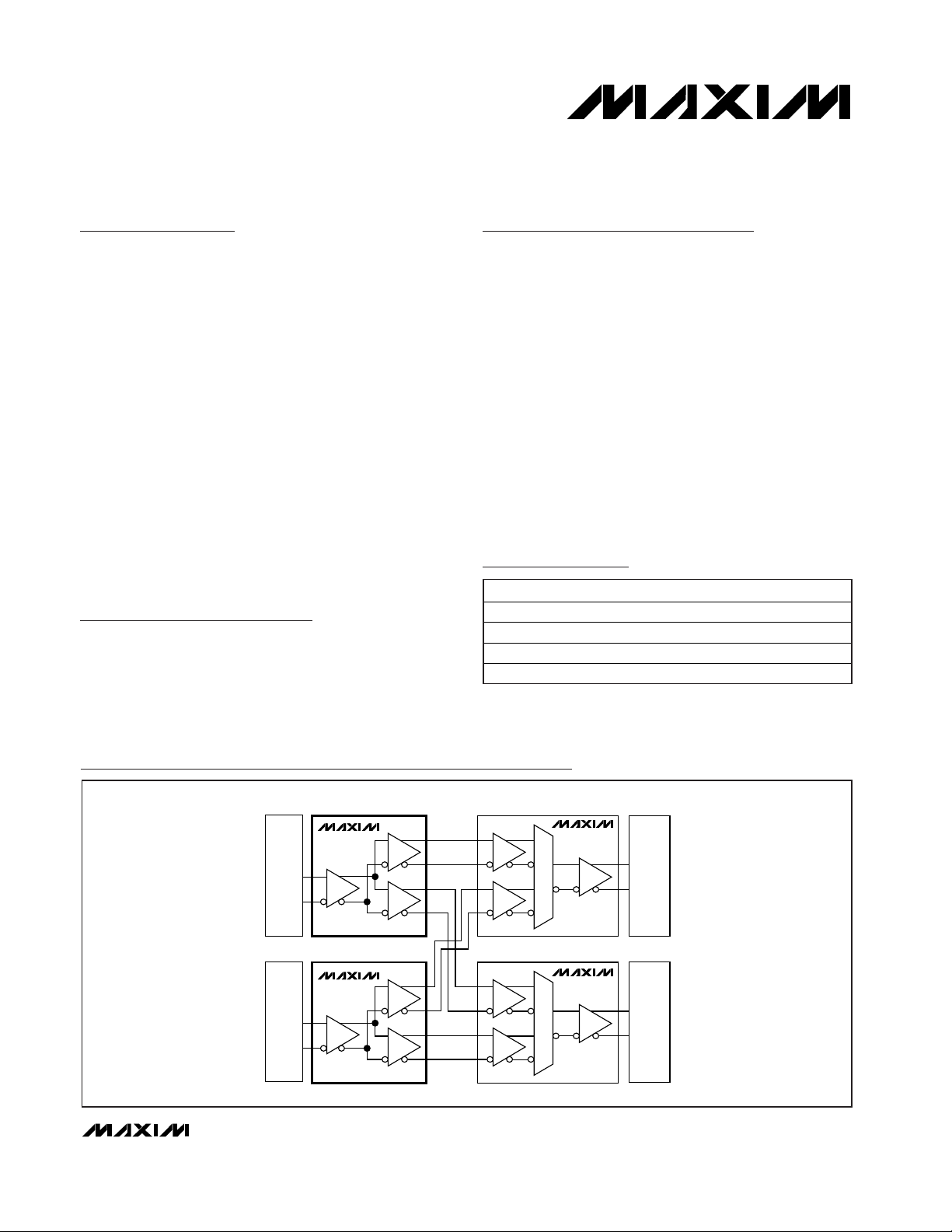
CLK IN
ASIC
CLOCK DISTRIBUTION
CLK IN
ASIC
CLK1
CLK2
MAX9174
MAX9174
MAX9176
MAX9176
Typical Application Circuit
19-2827; Rev 1; 4/04
For pricing, delivery, and ordering information, please contact Maxim/Dallas Direct! at
1-888-629-4642, or visit Maxim’s website at www.maxim-ic.com.
PART TEMP RANGE PIN-PACKAGE
MAX9174EUB -40°C to +85°C 10 µMAX
MAX9174ETB* -40°C to +85°C 10 Thin QFN-EP**
MAX9175EUB -40°C to +85°C 10 µMAX
MAX9175ETB* -40°C to +85°C 10 Thin QFN-EP**
*Future product—contact factory for availability.
**EP = Exposed paddle.
Functional Diagram and Pin Configurations appear at end
of data sheet.
Page 2
MAX9174/MAX9175
670MHz LVDS-to-LVDS and Anything-to-LVDS
1:2 Splitters
2 _______________________________________________________________________________________
ABSOLUTE MAXIMUM RATINGS
Stresses beyond those listed under “Absolute Maximum Ratings” may cause permanent damage to the device. These are stress ratings only, and functional
operation of the device at these or any other conditions beyond those indicated in the operational sections of the specifications is not implied. Exposure to
absolute maximum rating conditions for extended periods may affect device reliability.
VCCto GND..………………………………………...-0.3V to +4.0V
IN+, IN- to GND...........................................……...-0.3V to +4.0V
OUT_+, OUT_- to GND..........................................-0.3V to +4.0V
PD0, PD1 to GND.......................................-1.4V to (VCC+ 1.4V)
Single-Ended and Differential Output
Short-Circuit Duration (OUT_+, OUT_-) .....................Continuous
Continuous Power Dissipation (T
A
= +70°C)
10-Pin µMAX (derate 5.6mW/°C above +70°C) ...........444mW
10-Lead QFN (derate 24.4mW/°C above +70°C) ......1951mW
Maximum Junction Temperature .....................................+150°C
Storage Temperature Range .............................-65°C to +150°C
ESD Protection
Human Body Model (R
D
= 1.5kΩ, CS= 100pF)
IN+, IN-, OUT_+, OUT_-...............................................…±2kV
Other Pins (V
CC
, PD0, PD1) ...............................................2kV
IEC 61000-4-2 Level 4 (R
D
= 330Ω, CS= 150pF)
Contact Discharge IN+, IN-, OUT_+, OUT_- ...................±8kV
Air-Gap Discharge IN+, IN-, OUT_+, OUT_- .................±15kV
Lead Temperature (soldering, 10s) .................................+300°C
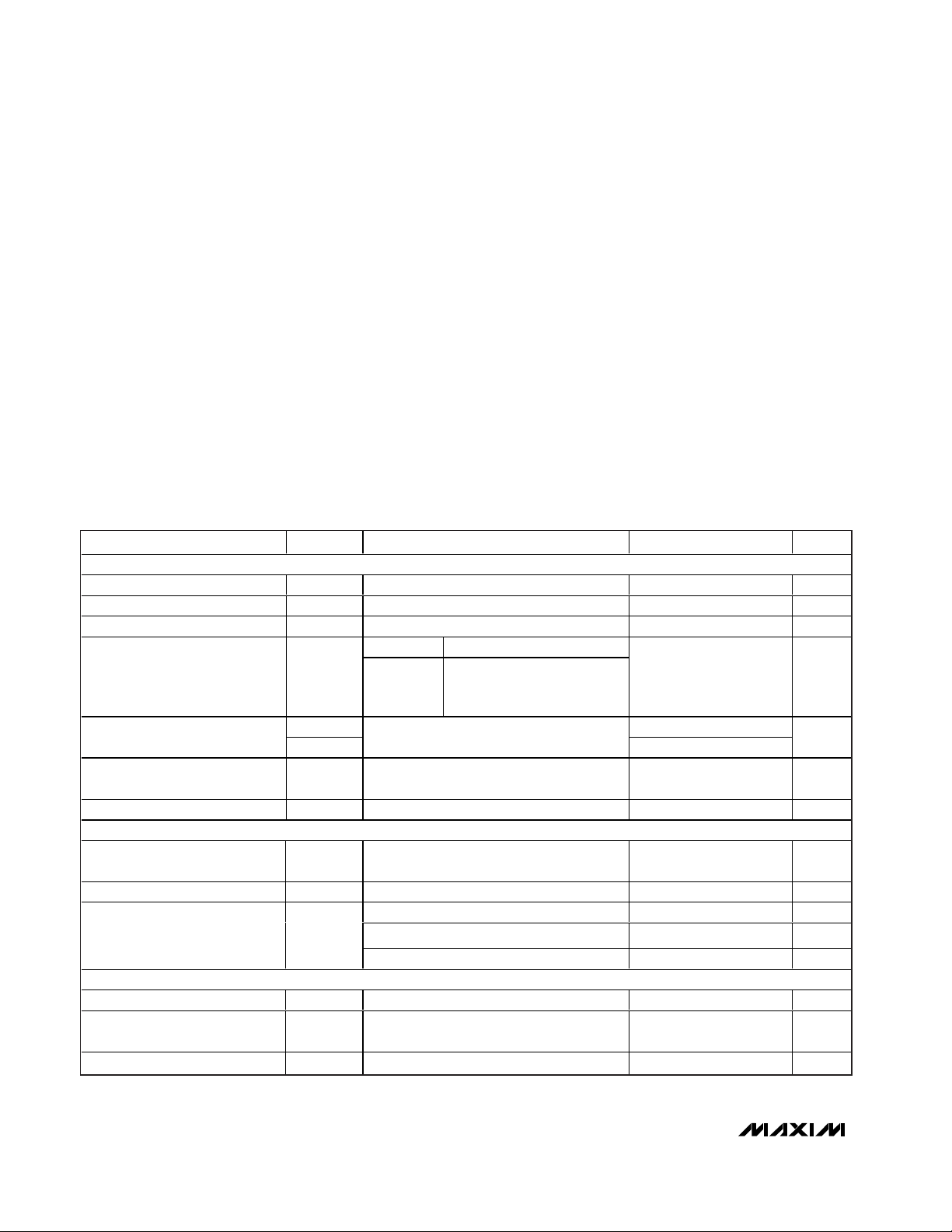
DC ELECTRICAL CHARACTERISTICS
(VCC= +3.0V to +3.6V, RL= 100Ω ±1%, PD_ = high, differential input voltage |VID| = 0.05V to 1.2V, MAX9174 input common-mode
voltage V
CM
= |VID/2| to (2.4V - |VID/2|), MAX9175 input common-mode voltage VCM= |VID/2| to (VCC- | VID/2|), TA= -40°C to
+85°C, unless otherwise noted. Typical values are at V
CC
= +3.3V, |VID| = 0.2V, VCM= +1.25V, TA= +25°C.) (Notes 1, 2, 3)
PARAMETER
CONDITIONS
UNITS
DIFFERENTIAL INPUT (IN+, IN-)
V
TH
+50 mV
Differential Input Low Threshold V
TL
-50 mV
Input Current
Figure 1 -20 +20 µA
MAX9174 V
CC
= 0V or open, Figure 1
Power-Off Input Current
I
IN+,
I
IN- MAX9175
V
IN+
= 3.6V or 0V, V
IN-
= 3.6V
or 0V, V
CC
= 0V or open,
Figure 1
-20 +20 µA
R
IN1
60 108
Fail-Safe Input Resistors
(MAX9174)
R
IN2
V
CC
= 3.6V, 0V or open, Figure 1
200 394
kΩ
Input Resistors
(MAX9175)
R
IN3
V
CC
= 3.6V, 0V or open, Figure 1 212 450 kΩ
Input Capacitance C
IN
IN+ or IN- to GND (Note 4) 4.5 pF
LVTTL/LVCMOS INPUTS (PPPPDDDD0000, PPPPDDDD1111)
Input High Voltage V
IH
2.0
V
CC
+
1
V
Input Low Voltage V
IL
V
-1.0V ≤ PD_ ≤ 0V
mA
0V ≤ PD_ ≤ V
CC
-20 +20 µAInput Current I
IN
VCC ≤ PD_ ≤ VCC + 1.0V
mA
LVDS OUTPUTS (OUT_+, OUT_-)
Differential Output Voltage V
OD
Figure 2 250
475 mV
Change in Differential Output
Voltage Between Logic States
∆V
OD
Figure 2
15 mV
Offset Voltage V
OS
Figure 3
V
SYMBOL
Differential Input High Threshold
MIN TYP MAX
I
IN
+,
I
IN
-
-1.0 +0.8
-1.5
1.125 1.29 1.375
393
1.0
+1.5
Page 3
MAX9174/MAX9175
670MHz LVDS-to-LVDS and Anything-to-LVDS
1:2 Splitters
_______________________________________________________________________________________ 3
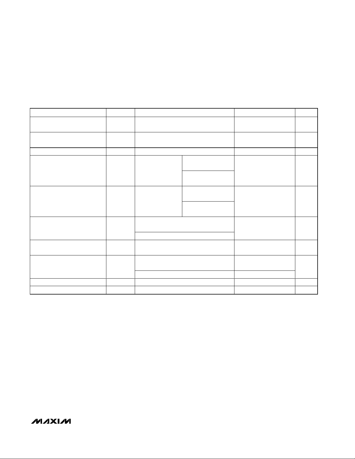
DC ELECTRICAL CHARACTERISTICS (continued)
(VCC= +3.0V to +3.6V, RL= 100Ω ±1%, PD_ = high, differential input voltage |VID| = 0.05V to 1.2V, MAX9174 input common-mode
voltage V
CM
= |VID/2| to (2.4V - |VID/2|), MAX9175 input common-mode voltage VCM= |VID/2| to (VCC- | VID/2|), TA= -40°C to
+85°C, unless otherwise noted. Typical values are at V
CC
= +3.3V, |VID| = 0.2V, VCM= +1.25V, TA= +25°C.) (Notes 1, 2, 3)
PARAMETER
CONDITIONS
Change in Offset Voltage
Between Logic States
∆V
OS
Figure 3
15 mV
Fail-Safe Differential Output
Voltage (MAX9174)
V
OD
Figure 2 250
475 mV
Differential Output Resistance R
DIFF
V
CC
= 3.6V or 0V 86
160 Ω
V
OUT_+
= open,
V
OUT_-
= 3.6V or 0V
Power-Down Single-Ended
Output Current
I
PD
PD_ = low
V
OUT_-
= open,
_
µA
V
OUT_+
= open,
_
Power-Off Single-Ended Output
Current
I
OFF
PD0, PD1 = low,
V
CC
= 0V or open
V
OUT_-
= open,
_
µA
VID = +50mV or -50mV, V
OUT_+
= 0V or
V
CC
Output Short-Circuit Current I
OS
_
-15 +15 mA
Differential Output Short-Circuit
Current Magnitude
I
OSD
15 mA
PD0 = VCC, PD1 = 0V or
PD0 = 0V, PD1 = V
CC
17 26
Supply Current I
CC
PD0 = Vcc, PD1 = Vcc 25 35
mA
Power-Down Supply Current I
CCPD
PD1, PD0
= 0V
20 µA
Output Capacitance C
O
OUT_+ or OUT_- to GND (Note 4) 5.2 pF
SYMBOL
MIN TYP MAX UNITS
1.0
393
119
-1.0 ±0.03 +1.0
V
OUT
V
OUT
V
OUT
VID = +50mV or -50mV, V
OUT
3.6V or 0V
+ =
3.6V or 0V
- =
3.6V or 0V
+ =
= 0V or V
-
-1.0 ±0.03 +1.0
CC
VID = +50mV or -50mV, VOD = 0V (Note 4)
0.5
Page 4
MAX9174/MAX9175
670MHz LVDS-to-LVDS and Anything-to-LVDS
1:2 Splitters
4 _______________________________________________________________________________________
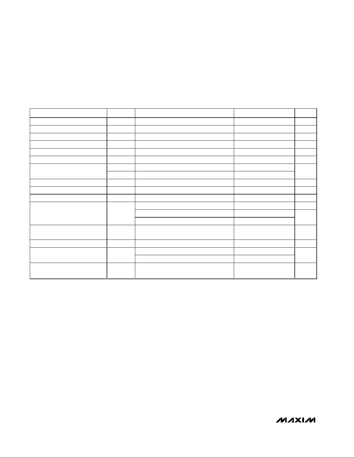
AC ELECTRICAL CHARACTERISTICS
(VCC= +3.0V to +3.6V, RL= 100Ω±1%, CL= 5pF, differential input voltage |VID| = 0.15V to 1.2V, MAX9174 input common-mode voltage, V
CM
= |VID/2| to (2.4V - |VID/2|), MAX9175 input common-mode voltage VCM= |VID/2| to (VCC- |VID/2|), PD_ = high, TA= -40°C
to +85°C, unless otherwise noted. Typical values are at V
CC
= +3.3V, |VID| = 0.2V, VCM= +1.25V, TA= +25°C.) (Notes 5, 6, 7)
PARAMETER
CONDITIONS
UNITS
High-to-Low Propagation Delay t
PHL
Figures 4, 5
ns
Low-to-High Propagation Delay t
PLH
Figures 4, 5
ns
Added Deterministic Jitter t
DJ
Figures 4, 5 (Note 8) 80
ps
(P-P)
Added Random Jitter t
RJ
Figures 4, 5 1.0
ps
(RMS)
Pulse Skew t
PLH
- t
PHL
t
SKP
Figures 4, 5 10
ps
Output-to-Output Skew t
SKOO
Figure 6 14 45 ps
t
SKPP1
Figures 4, 5 (Note 9) 0.4 1.3
Part-to-Part Skew
t
SKPP2
Figures 4, 5 (Note 10) 1.9
ns
Rise Time t
R
Figures 4, 5
ps
Fall Time t
F
Figures 4, 5
ps
Power-Down Time t
PD
Figures 7, 8 10 13 ns
PD0, PD1 = L → H, Figures 7, 8
18 35 µs
PD0 = H, PD1 = L → H, Figures 7, 8 92
Power-Up Time t
PU
PD1 = H, PD0 L → H, Figures 7, 8 92
ns
Maximum Data Rate D
RMAX
Figures 4, 5, VOD ≥ 250mV
(Note 11)
Mbps
Maximum Switching Frequency f
MAX
Figures 4, 5, VOD ≥ 250mV (Note 11)
MHz
fIN = 670MHz 55 65
Switching Supply Current I
CCSW
fIN = 155MHz 35 44
mA
PRBS Supply Current I
CCPR
DR = 800Mbps, 223 - 1 PRBS input 37 46 mA
Note 1: Current into a pin is defined as positive. Current out of a pin is defined as negative. All voltages are referenced to ground
except V
TH
, VTL, VID, VOD, and ∆VOD.
Note 2: Maximum and minimum limits over temperature are guaranteed by design and characterization. Devices are 100% tested at
T
A
= +25°C.
Note 3: Tolerance on all external resistors (including figures) is ±1%.
Note 4: Guaranteed by design.
Note 5: AC parameters are guaranteed by design and characterization and are not production tested. Limits are set at ±6 sigma.
Note 6: C
L
includes scope probe and test jig capacitance.
Note 7: Pulse-generator output for differential inputs IN+, IN- (unless otherwise noted): f = 670MHz, 50% duty cycle, R
O
= 50Ω, tR=
700ps, and t
F
= 700ps (0% to 100%). Pulse-generator output for single-ended inputs PD0, PD1: tR= tF= 1.5ns (0.2VCCto
0.8V
CC
), 50% duty cycle, VOH= VCC+ 1.0V settling to VCC, VOL= -1.0V settling to zero, f = 10kHz.
Note 8: Pulse-generator output for t
DJ
: |VOD| = 0.15V, VOS= 1.25V, data rate 800Mbps, 223- 1 PRBS, RO= 50Ω, tR= 700ps, and t
F
= 700ps (0% to 100%).
Note 9: t
SKPP1
is the magnitude of the difference of any differential propagation delays between devices operating under identical
conditions.
Note 10: t
SKPP2
is the magnitude of the difference of any differential propagation delays between devices operating over rated con-
ditions.
Note 11: Meets all AC specifications.
SYMBOL
MIN TYP MAX
1.33 2.38 3.23
1.33 2.39 3.23
110 257 365
110 252 365
141
103
103
800
670
Page 5
MAX9174/MAX9175
670MHz LVDS-to-LVDS and Anything-to-LVDS
1:2 Splitters
_______________________________________________________________________________________ 5
SUPPLY CURRENT vs. TEMPERATURE
MAX9174 toc01
TEMPERATURE (°C)
SUPPLY CURRENT (mA)
603510-15
33
34
35
36
37
38
32
-40 85
fIN = 155MHz
DIFFERENTIAL OUTPUT VOLTAGE
vs. FREQUENCY
MAX9174 toc02
FREQUENCY (MHz)
DIFFERENTIAL OUTPUT VOLTAGE (mV)
700600400 500200 300100
310
320
330
340
350
360
370
380
390
400
410
300
0 800
OUTPUT RISE/FALL TIME
vs. TEMPERATURE
MAX9174 toc03
TEMPERATURE (°C)
RISE/FALL TIME (ps)
603510-15
220
230
240
250
260
270
280
290
300
210
-40 85
fIN = 155MHz
t
R
t
F
DIFFERENTIAL PROPAGATION DELAY
vs. TEMPERATURE
MAX9174 toc04
TEMPERATURE (°C)
DIFFERENTIAL PROPAGATION DELAY (ns)
603510-15
2.2
2.3
2.4
2.5
2.6
2.7
2.8
2.9
3.0
2.0
2.1
-40 85
fIN = 155MHz
t
PHL
t
PLH
OUTPUT-TO-OUTPUT SKEW
vs. TEMPERATURE
MAX9174 toc05
TEMPERATURE (°C)
OUTPUT-TO-OUTPUT SKEW (ps)
603510-15
2
4
6
8
10
12
14
16
18
20
0
-40 85
fIN = 155MHz
SUPPLY CURRENT vs. FREQUENCY
MAX9174 toc06
FREQUENCY (MHz)
SUPPLY CURRENT (mA)
700600100 200 300 400 500
25
30
35
40
45
50
55
60
20
0 800
SUPPLY CURRENT vs. DATA RATE
MAX9174 toc07
DATA RATE (Mbps)
SUPPLY CURRENT (mA)
700600500400300200100
25
30
35
40
45
15
20
0 800
PRBS 223 - 1
SUPPLY CURRENT vs. SUPPLY VOLTAGE
MAX9174 toc08
SUPPLY VOLTAGE (V)
SUPPLY CURRENT (mA)
3.53.43.33.23.1
31
32
33
34
35
36
37
38
39
40
30
3.0 3.6
fIN = 155MHz
OUTPUT RISE/FALL TIME
vs. SUPPLY VOLTAGE
MAX9174 toc09
SUPPLY VOLTAGE (V)
RISE/FALL TIME (ps)
3.53.43.33.23.1
210
220
230
240
250
260
270
280
290
300
200
3.0 3.6
fIN = 155MHz
t
F
t
R
Typical Operating Characteristics
((MAX9174) VCC= +3.3V, |VID| = 0.15V, VCM= 1.25V, TA= +25°C, RL= 100Ω ±1%, CL= 5pf, PD_ = VCC, unless otherwise noted.)
Page 6

MAX9174/MAX9175
670MHz LVDS-to-LVDS and Anything-to-LVDS
1:2 Splitters
6 _______________________________________________________________________________________
Typical Operating Characteristics (continued)
((MAX9174) VCC= +3.3V, |VID| = 0.15V, VCM= 1.25V, TA= +25°C, RL= 100Ω ±1%, CL= 5pf, PD_ = VCC, unless otherwise noted.)
DIFFERENTIAL PROPAGATION DELAY
vs. SUPPLY VOLTAGE
MAX9174 toc10
SUPPLY VOLTAGE (V)
DIFFERENTIAL PROPAGATION DELAY (ns)
3.53.43.33.23.1
2.1
2.2
2.3
2.4
2.5
2.6
2.7
2.8
2.9
3.0
2.0
3.0 3.6
fIN = 155MHz
t
PLH
t
PHL
OUTPUT-TO-OUTPUT SKEW
vs. SUPPLY VOLTAGE
MAX9174 toc11
SUPPLY VOLTAGE (V)
OUTPUT-TO-OUTPUT SKEW (ps)
3.53.43.33.23.1
1
2
3
4
5
6
7
8
9
10
0
3.0 3.6
fIN = 155MHz
DIFFERENTIAL OUTPUT VOLTAGE
vs. LOAD RESISTANCE
MAX9174 toc12
LOAD RESISTANCE (Ω)
DIFFERENTIAL OUTPUT VOLTAGE (mV)
14013012011010090807060
250
300
350
400
450
500
200
50 150
PROPAGATION DELAY
vs. INPUT COMMON-MODE VOLTAGE
MAX9174 toc13a
INPUT COMMON-MODE VOLTAGE (V)
PROPAGATION DELAY (ns)
1.5750.825
2.3
2.4
2.5
2.6
2.7
2.8
2.2
0.075 2.325
MAX9174
f
IN
= 155MHz
t
PHL
t
PLH
PROPAGATION DELAY
vs. INPUT COMMON-MODE VOLTAGE
MAX9174 toc13b
INPUT COMMON-MODE VOLTAGE (V)
PROPAGATION DELAY (ns)
2.7752.3251.425 1.8750.9750.525
2.1
2.2
2.3
2.4
2.5
2.6
2.7
2.8
2.9
3.0
2.0
0.075 3.225
fIN = 155MHz
t
PHL
t
PLH
OUTPUT-TO-OUTPUT SKEW
vs. INPUT COMMON-MODE VOLTAGE
MAX9174 toc14a
INPUT COMMON-MODE VOLTAGE (V)
OUTPUT-TO-OUTPUT SKEW (ps)
1.5750.825
6.2
6.4
6.6
6.8
7.0
7.2
7.4
7.6
7.8
8.0
6.0
0.075 2.325
MAX9174
f
IN
= 155MHz
OUTPUT-TO-OUTPUT SKEW
vs. INPUT COMMON-MODE VOLTAGE
MAX9174 toc14b
INPUT COMMON-MODE VOLTAGE (V)
OUTPUT-TO-OUTPUT SKEW (ps)
2.7752.3250.525 0.975 1.425 1.875
2.5
3.0
3.5
4.0
4.5
5.0
5.5
6.0
2.0
0.075 3.225
MAX9175
f
IN
= 155MHz
Page 7

Detailed Description
The MAX9174/MAX9175 are 670MHz, low-jitter, lowskew 1:2 splitters ideal for protection switching, loopback, and clock and signal distribution. The devices
feature ultra-low 80ps
P-P
deterministic jitter (max) that
ensures reliable operation in high-speed links that are
highly sensitive to timing error.
The MAX9174 has a fail-safe LVDS input and LVDS outputs. The MAX9175 has an anything differential input
(CML/LVDS/LVPECL) and LVDS outputs. The outputs
can be put into high impedance using the power-down
inputs. The MAX9174 features a fail-safe circuit that drives the outputs high when the input is open, undriven
and shorted, or undriven and terminated. The MAX9175
has a bias circuit that forces the outputs high when the
input is open. The power-down inputs are compatible
with standard LVTTL/LVCMOS logic.
The power-down inputs tolerate undershoot of -1V and
overshoot of VCC + 1V. The MAX9174/MAX9175 are
available in 10-pin µMAX and 10-lead thin QFN packages, and operate from a single +3.3V supply over the
-40°C to +85°C temperature range.
Current-Mode LVDS Outputs
The LVDS outputs use a current-steering configuration.
This approach results in less ground bounce and less
output ringing, enhancing noise margin and system
speed performance.
A differential output voltage is produced by steering
current through the parallel combination of the integrated differential output resistor and transmission line
impedance/termination resistor. When driving a 100Ω
termination resistor, a differential voltage of 250mV to
475mV is produced. For loads greater than 100Ω, the
output voltage is larger, and for loads less than 100Ω,
the output voltage is smaller. See the Differential Output
Voltage vs. Load Resistance curve in Typical Operating
Characteristics for more information. The outputs are
short-circuit current limited for single-ended and differential shorts.
MAX9174 Input Fail-Safe
The fail-safe feature of the MAX9174 sets the outputs
high when the differential input is:
• Open
• Undriven and shorted
• Undriven and terminated
Without a fail-safe circuit, when the input is undriven,
noise at the input may switch the outputs and it may
appear to the system that data is being sent. Open or
undriven terminated input conditions can occur when a
cable is disconnected or cut, or when a driver output is
in high impedance. A shorted input can occur because
of a cable failure.
MAX9174/MAX9175
670MHz LVDS-to-LVDS and Anything-to-LVDS
1:2 Splitters
_______________________________________________________________________________________ 7
Pin Description
PIN
µMAX QFN
NAME FUNCTION
11IN+ Noninverting Differential Input
22IN- Inverting Differential Input
33GND Ground
44PD1
LVTTL/LVCMOS Input. OUT1+, OUT1- are high impedance to ground when PD1 is low.
Internal pulldown resistor to GND.
55PD0
LVTTL/LVCMOS Input. OUT0+, OUT0- are high impedance to ground when PD0 is low.
Internal pulldown resistor to GND.
66OUT0- Inverting LVDS Output 0
77OUT0+ Noninverting LVDS Output 0
88VCCPower Supply
99OUT1- Inverting LVDS Output 1
10 10 OUT1+ Noninverting LVDS Output 1
—EP
Exposed
Pad
Exposed Pad. Solder to ground.
Page 8

MAX9174/MAX9175
When the input is driven with a differential signal of |VID|
= 50mV to 1.2V within a voltage range of 0 to 2.4V, the
fail-safe circuit is not activated. If the input is open,
undriven and shorted, or undriven and terminated, an
internal resistor in the fail-safe circuit pulls the input
above VCC - 0.3V, activating the fail-safe circuit and
forcing the outputs high (Figure 1).
Overshoot and Undershoot Voltage
Protection
The MAX9174/MAX9175 are designed to protect the
power-down inputs (PD0 and PD1) against latchup due
to transient overshoot and undershoot voltage. If the
input voltage goes above VCC or below GND by up to
1V, an internal circuit limits input current to 1.5mA.
Applications Information
Power-Supply Bypassing
Bypass the VCCpin with high-frequency surface-mount
ceramic 0.1µF and 0.001µF capacitors in parallel as
close to the device as possible, with the smaller valued
capacitor closest to VCC.
Differential Traces
Input and output trace characteristics affect the performance of the MAX9174/MAX9175. Use controlledimpedance differential traces (100Ω typ). To reduce
radiated noise and ensure that noise couples as common mode, route the differential input and output signals within a pair close together. Reduce skew by
matching the electrical length of the two signal paths
that make up the differential pair. Excessive skew can
result in a degradation of magnetic field cancellation.
Maintain a constant distance between the differential
traces to avoid discontinuities in differential impedance.
Minimize the number of vias to further prevent impedance discontinuities.
Cables and Connectors
Interconnect for LVDS typically has a controlled differential impedance of 100Ω. Use cables and connectors
that have matched differential impedance to minimize
impedance discontinuities.
Avoid the use of unbalanced cables such as ribbon or
simple coaxial cable. Balanced cables such as twisted
pair offer superior signal quality and tend to generate
less EMI due to magnetic field canceling effects.
Balanced cables pick up noise as common mode,
which is rejected by the LVDS receiver.
Termination
The MAX9174/MAX9175 require external input and output termination resistors. For LVDS, connect an input
termination resistor across the differential input and at
the far end of the interconnect driven by the LVDS outputs. Place the input termination resistor as close to the
receiver input as possible. Termination resistors should
match the differential impedance of the transmission
line. Use 1% surface-mount resistors.
670MHz LVDS-to-LVDS and Anything-to-LVDS
1:2 Splitters
8 _______________________________________________________________________________________
INPUT OUTPUTS
(IN+) - (IN-) (OUT_+) - (OUT_-)
≥ +50mV H
≤ -50mV L
-50mV < VID < +50mV Indeterminate
MAX9175
Open
MAX9174
Open, undriven
short, or undriven
H
Table 1. Input Function Table
PPPPDDDD11
11
PPPPDDDD00
00
OUT_+, OUT_-
HHBoth outputs enabled
Shutdown to minimum power,
outputs high impedance to ground
High
OUT0 enabled, OUT1 high
impedance to ground
High
OUT1 enabled, OUT0 high
impedance to ground
Table 2. Power-Down Function Table
IN+
TO
OUTPUT
IN-
IN+
IN-
MAX9175 INPUTMAX9174 INTERNAL FAIL-SAFE CIRCUIT
DIFFERENTIAL
RCVR
COMPARATOR
R
IN3
R
IN3
VCC - 0.3V
V
CC
R
IN2
R
IN1
R
IN1
V
CC
Figure 1. Input Structure
parallel termination
L or open L or open
L or open
L or open
Page 9

The MAX9174/MAX9175 feature an integrated differential output resistor. This resistor reduces jitter by damping reflections produced by a mismatch between the
transmission line and termination resistor at the far end
of the interconnect.
Board Layout
Separate the differential and single-ended signals to
reduce crosstalk. A four-layer printed circuit board with
separate layers for power, ground, differential signals,
and single-ended logic signals is recommended.
Separate the differential signals from the logic signals
with power and ground planes for best results.
IEC 61000-4-2 Level 4
ESD Protection
The IEC 61000-4-2 standard (Figure 9) specifies ESD
tolerance for electronic systems. The IEC 61000-4-2
model specifies a 150pF capacitor that is discharged
into the device through a 330Ω resistor. The MAX9174/
MAX9175 differential inputs and outputs are rated for
IEC 61000-4-2 level 4 (±8kV Contact Discharge and
±15kV Air-Gap Discharge). The Human Body Model
(HBM, Figure 10) specifies a 100pF capacitor that is
discharged into the device through a 1.5kΩ resistor.
IEC 61000-4-2 level 4 discharges higher peak current
and more energy than the HBM due to the lower series
resistance and larger capacitor.
MAX9174/MAX9175
670MHz LVDS-to-LVDS and Anything-to-LVDS
1:2 Splitters
_______________________________________________________________________________________ 9
V
TEST
= 0 TO V
CC
V
OD
IN+
5kΩ
5kΩ
1.25V
1.20V
1.25V
1.20V
IN-
R
L
OUT_ -
OUT_+
Figure 2. VODTest Circuit
IN+
1.25V
1.20V
1.25V
1.20V
IN-
R
L
/2
RL/2
OUT_ -
VOS
OUT_+
Figure 3. VOSTest Circuit
PULSE
GENERATOR
50Ω
C
L
50Ω
C
L
V
TEST
= 0 TO V
CC
IN+
5kΩ
5kΩ
IN-
R
L
OUT0-
OUT0+
C
L
C
L
5kΩ
5kΩ
R
L
OUT1-
OUT1+
Figure 4. Transition Time, Propagation Delay, and Output-to-Output Skew Test Circuit
Page 10

MAX9174/MAX9175
670MHz LVDS-to-LVDS and Anything-to-LVDS
1:2 Splitters
10 ______________________________________________________________________________________
IN+
IN-
OUT0+
OUT0-
OUT1+
OUT1-
t
SKOO
t
SKOO
Figure 6. Output-to-Output Skew
t
PHL
t
PLH
80%
20%
20%
80%
0V
V
OD-
V
OD+
0V
V
OS
= ((V
OUT_
+) + (V
OUT_-
))/2
IN-
IN+
OUT_-
(OUT_+) - (OUT_-)
OUT_+
t
F
t
R
Figure 5. Transition Time and Propagation Delay Timing
Page 11

MAX9174/MAX9175
670MHz LVDS-to-LVDS and Anything-to-LVDS
1:2 Splitters
______________________________________________________________________________________ 11
50%
PD_
50%
50%
1.25V
1.25V
50%
OUT_+ WHEN V
ID
= +50mV
OUT_- WHEN V
ID
= -50mV
OUT_+ WHEN V
ID
= -50mV
OUT_- WHEN V
ID
= +50mV
t
PU
t
PU
t
PD
t
PD
VCC + 1V
V
CC
V
OH
V
OL
VCC/2
0
-1.0V
Figure 7. Power-Up/Down Delay Waveform
OUT1+
OUT1-
OUT0+
OUT0-
IN+
IN-
MAX9174
MAX9175
1.25V
1.20V
1.25V
1.20V
R
L
/2
RL/2
1.25V
RL/2
RL/2
1.25V
PULSE
GENERATOR
50Ω
Figure 8. Power-Up/Down Delay Test Circuit
Page 12

MAX9174/MAX9175
670MHz LVDS-to-LVDS and Anything-to-LVDS
1:2 Splitters
12 ______________________________________________________________________________________
CHARGE-CURRENT-
LIMIT RESISTOR
DISCHARGE
RESISTANCE
STORAGE
CAPACITOR
C
s
150pF
R
C
50Ω TO 100Ω
R
D
330Ω
HIGH-
VOLTAGE
DC
SOURCE
DEVICE
UNDER
TEST
Figure 9. IEC 61000-4-2 Contact Discharge ESD Test Model
CHARGE-CURRENT-
LIMIT RESISTOR
DISCHARGE
RESISTANCE
STORAGE
CAPACITOR
C
s
100pF
R
C
1MΩ
R
D
1.5kΩ
HIGH-
VOLTAGE
DC
SOURCE
DEVICE
UNDER
TEST
Figure 10. Human Body ESD Test Model
LVDS
DRIVER 1
LVDS
DRIVER 0
OUT1+
OUT1-
OUT0+
OUT0-
IN+
IN-
PD1
PD0
MAX9174
MAX9175
DIFFERENTIAL
RECEIVER
Functional Diagram
1
2
3
4
5
10
9
8
7
6
OUT1+
OUT1-
V
CC
OUT0+PD1
GND
IN-
IN+
MAX9174
MAX9175
µMAX
TOP VIEW
OUT0-
EXPOSED PAD
10
9
8
7
6
OUT1+
OUT1-
V
CC
OUT0+
OUT0- PD0
1
2
3
45PD1
GND
IN-
IN+
PD0
MAX9174
MAX9175
THIN QFN
(LEADS UNDER PACKAGE)
Pin Configurations
Chip Information
TRANSISTOR COUNT: 693
PROCESS: CMOS
Page 13

MAX9174/MAX9175
670MHz LVDS-to-LVDS and Anything-to-LVDS
1:2 Splitters
______________________________________________________________________________________ 13
Package Information
(The package drawing(s) in this data sheet may not reflect the most current specifications. For the latest package outline information,
go to www.maxim-ic.com/packages
.)
10LUMAX.EPS
PACKAGE OUTLINE, 10L uMAX/uSOP
1
1
21-0061
I
REV.DOCUMENT CONTROL NO.APPROVAL
PROPRIETARY INFORMATION
TITLE:
TOP VIEW
FRONT VIEW
1
0.498 REF
0.0196 REF
S
6∞
SIDE VIEW
α
BOTTOM VIEW
0∞ 0∞ 6∞
0.037 REF
0.0078
MAX
0.006
0.043
0.118
0.120
0.199
0.0275
0.118
0.0106
0.120
0.0197 BSC
INCHES
1
10
L1
0.0035
0.007
e
c
b
0.187
0.0157
0.114
H
L
E2
DIM
0.116
0.114
0.116
0.002
D2
E1
A1
D1
MIN
-A
0.940 REF
0.500 BSC
0.090
0.177
4.75
2.89
0.40
0.200
0.270
5.05
0.70
3.00
MILLIMETERS
0.05
2.89
2.95
2.95
-
MIN
3.00
3.05
0.15
3.05
MAX
1.10
10
0.6±0.1
0.6±0.1
ÿ 0.50±0.1
H
4X S
e
D2
D1
b
A2
A
E2
E1
L
L1
c
α
GAGE PLANE
A2 0.030 0.037 0.75 0.95
A1
Page 14

MAX9174/MAX9175
670MHz LVDS-to-LVDS and Anything-to-LVDS
1:2 Splitters
Maxim cannot assume responsibility for use of any circuitry other than circuitry entirely embodied in a Maxim product. No circuit patent licenses are
implied. Maxim reserves the right to change the circuitry and specifications without notice at any time.
14 ____________________Maxim Integrated Products, 120 San Gabriel Drive, Sunnyvale, CA 94086 408-737-7600
© 2004 Maxim Integrated Products Printed USA is a registered trademark of Maxim Integrated Products.
Package Information (continued)
(The package drawing(s) in this data sheet may not reflect the most current specifications. For the latest package outline information,
go to www.maxim-ic.com/packages
.)
6, 8, &10L, DFN THIN.EPS
PROPRIETARY INFORMATION
TITLE:
APPROVAL
DOCUMENT CONTROL NO. REV.
2
1
PACKAGE OUTLINE, 6, 8 & 10L,
TDFN, EXPOSED PAD, 3x3x0.80 mm
21-0137 D
L
C
L
C
SEMICONDUCTOR
DALLAS
A2
A
PIN 1
INDEX
AREA
D
E
A1
D2
b
E2
[(N/2)-1] x e
REF.
e
k
1N1
L
e
L
A
L
PIN 1 ID
C0.35
DETAIL A
e
NUMBER OF LEADS SHOWN ARE FOR REFERENCE ONLY
DOCUMENT CONTROL NO.APPROVAL
TITLE:
PROPRIETARY INFORMATION
REV.
2
2
COMMON DIMENSIONS
SYMBOL
MIN. MAX.
A
0.70 0.80
D
2.90 3.10
E
2.90 3.10
A1
0.00 0.05
L
0.20 0.40
PKG. CODE
6
N
T633-1 1.50±0.10D22.30±0.10
E2
0.95 BSCeMO229 / WEEA
JEDEC SPEC
0.40±0.05b1.90 REF
[(N/2)-1] x e
1.50±0.10
MO229 / WEEC
1.95 REF0.30±0.05
0.65 BSC
2.30±0.10T833-1 8
PACKAGE VARIATIONS
21-0137
0.25±0.05 2.00 REFMO229 / WEED-30.50 BSC1.50±0.10 2.30±0.1010T1033-1
0.25 MIN.
k
A2 0.20 REF.
D
SEMICONDUCTOR
DALLAS
PACKAGE OUTLINE, 6, 8 & 10L,
TDFN, EXPOSED PAD, 3x3x0.80 mm
 Loading...