

Page 1
MAX9173
Quad LVDS Line Receiver with Flow-Through
Pinout and “In-Path” Fail-Safe
________________________________________________________________ Maxim Integrated Products 1
19-2595; Rev 0; 10/02
For pricing, delivery, and ordering information, please contact Maxim/Dallas Direct! at
1-888-629-4642, or visit Maxim’s website at www.maxim-ic.com.
General Description
The MAX9173 quad low-voltage differential signaling
(LVDS) line receiver is ideal for applications requiring
high data rates, low power, and low noise. The
MAX9173 is guaranteed to receive data at speeds up
to 500Mbps (250MHz) over controlled-impedance
media of approximately 100Ω. The transmission media
can be printed circuit (PC) board traces or cables.
The MAX9173 accepts four LVDS differential inputs and
translates them to LVCMOS/LVTTL outputs. The
MAX9173 inputs are high impedance and require an
external termination resistor when used in a point-topoint connection.
The device supports a wide common-mode input range
of 0.05V to VCC- 0.05V, allowing for ground potential
differences and common-mode noise between the driver and the receiver. A fail-safe feature sets the output
high when the inputs are open, or when the inputs are
undriven and shorted or undriven and parallel terminated. The EN and EN inputs control the high-impedance
outputs. The enables are common to all four receivers.
Inputs conform to the ANSI TIA/EIA-644 LVDS standard. The flow-through pinout simplifies board layout
and reduces crosstalk by separating the LVDS inputs
and LVCMOS/LVTTL outputs. The MAX9173 operates
from a single 3.3V supply, and is specified for operation from -40°C to +85°C. Refer to the MAX9121/
MAX9122 data sheet for lower jitter quad LVDS
receivers with parallel fail-safe. Refer to the MAX9123
data sheet for a quad LVDS line driver with flowthrough pinout.
The device is available in 16-pin TSSOP, SO, and
space-saving thin QFN packages.
Applications
Digital Copiers
Laser Printers
Cellular Phone Base Stations
Network Switches/Routers
Backplane Interconnect
Clock Distribution
LCD Displays
Telecom Switching Equipment
Features
♦ Accepts LVDS and LVPECL Inputs
♦ Fully Compatible with DS90LV048A
♦ Low 1.0mA (max) Disable Supply Current
♦ In-Path Fail-Safe Circuitry
♦ Flow-Through Pinout
Simplifies PC Board Layout
Reduces Crosstalk
♦ Guaranteed 500Mbps Data Rate
♦ 400ps Pulse Skew (max)
♦ Conforms to ANSI TIA/EIA-644 LVDS Standard
♦ High-Impedance LVDS Inputs when Powered-Off
♦ Available in Tiny 3mm x 3mm QFN Package
Pin Configurations and Functional Diagram appear at end of
data sheet.
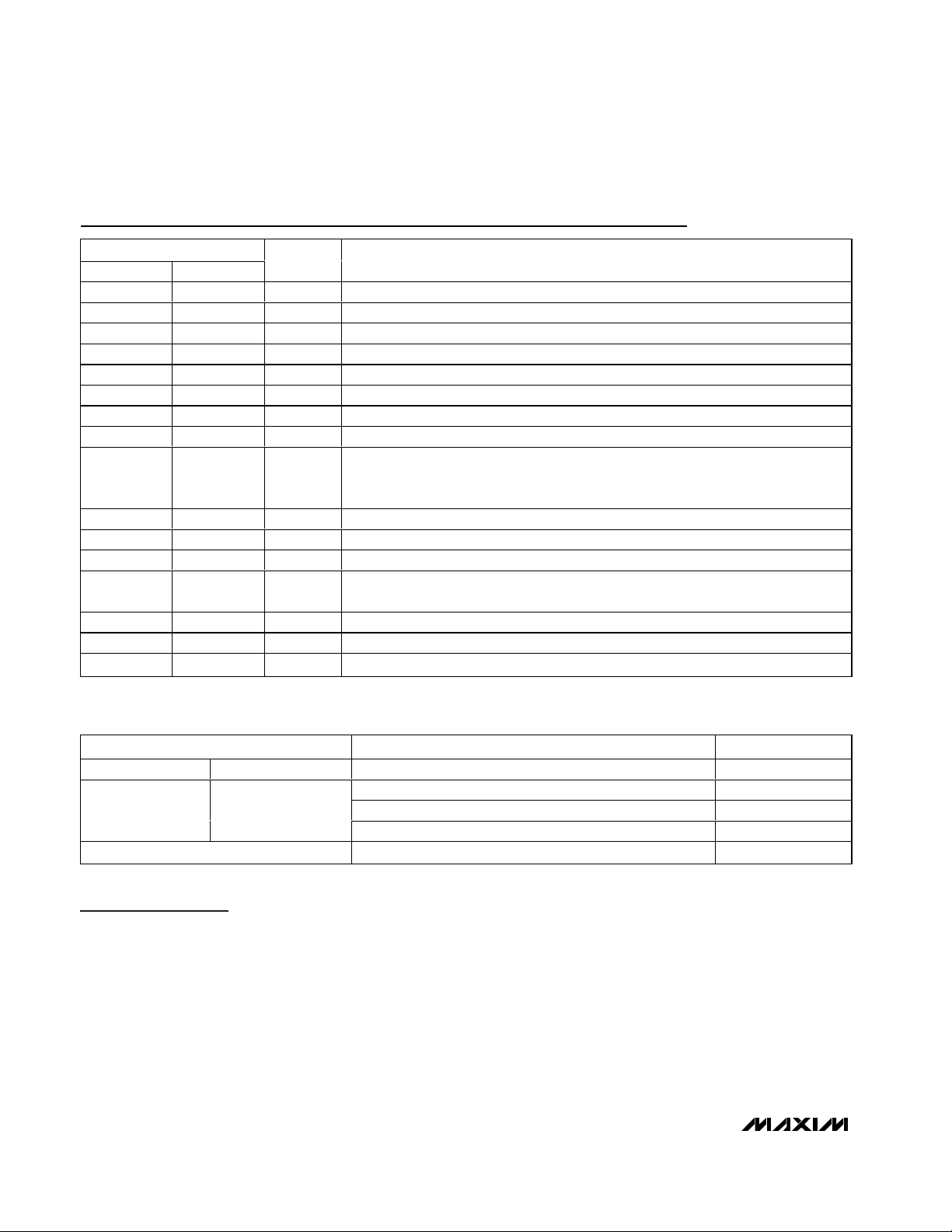
Ordering Information
*Future product. Contact factory for availability.
**EP = Exposed pad.
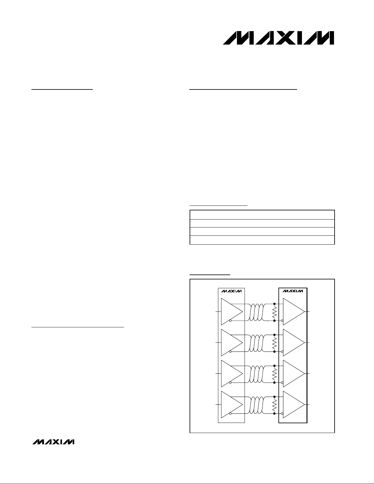
MAX9123
MAX9173
100Ω
100Ω
100Ω
100Ω
Rx
LVDS SIGNALS
100Ω SHIELDED TWISTED CABLE OR MICROSTRIP BOARD TRACES
LVTTL/LVCMOS
DATA INPUTS
LVTTL/LVCMOS
DATA OUTPUTS
Rx
Rx
Rx
Tx
Tx
Tx
Tx
Typical Operating Circuit
PART TEMP RANGE PIN-PACKAGE
MAX9173EUE -40°C to +85°C 16 TSSOP
MAX9173ESE -40°C to +85°C 16 SO
MAX9173ETE* -40°C to +85°C 16 Thin QFN-EP**
Page 2
MAX9173
Quad LVDS Line Receiver with Flow-Through
Pinout and “In-Path” Fail-Safe
2 _______________________________________________________________________________________
ABSOLUTE MAXIMUM RATINGS
Stresses beyond those listed under “Absolute Maximum Ratings” may cause permanent damage to the device. These are stress ratings only, and functional
operation of the device at these or any other conditions beyond those indicated in the operational sections of the specifications is not implied. Exposure to
absolute maximum rating conditions for extended periods may affect device reliability.
VCCto GND ..........................................................-0.3V to +4.0V
IN_+, IN_- to GND .................................................-0.3V to +4.0V
OUT_, EN, EN to GND................................-0.3V to (V
CC
+ 0.3V)
Continuous Power Dissipation (T
A
= +70°C)
16-Pin TSSOP (derate 9.4mW/°C above T
A
= +70°C)..755mW
16-Pin SO (derate 8.7mW/°C above T
A
= +70°C) ........696mW
16-Pin QFN (derate 14.7mW/°C above T
A
= +70°C)..1177mW
Junction Temperature......................................................+150°C
Storage Temperature Range .............................-65°C to +150°C
ESD Protection (Human Body Model, IN_+, IN_-) ............±7.0kV
Lead Temperature (soldering, 10s) .................................+300°C
DC ELECTRICAL CHARACTERISTICS
(VCC= 3.0V to 3.6V, differential input voltage |VID| = 0.1V to 1.2V, common-mode input voltage VCM= |VID/2| to VCC- |VID/2|, outputs
enabled, and T
A
= -40°C to +85°C. Typical values are at VCC= 3.3V, VCM= 1.2V, |VID| = 0.2V, and TA= +25°C, unless otherwise
noted.) (Notes 1, 2)
LVDS INPUTS (IN_+, IN_-)
Differential Input High Threshold V
Differential Input Low Threshold V
Input Current (Noninverting Input) I
Power-Off Input Current
(Noninverting Input)
Input Current (Inverting Input) I
Power-Off Input Current
(Inverting Input)
LVCMOS/LVTTL OUTPUTS (OUT_)
Output High Voltage (Table 1) V
Output Low Voltage V
Output Short-Circuit Current I
Output High-Impedance Current I
LOGIC INPUTS (EN, EN)
Input High Voltage V
Input Low Voltage V
Input Current I
Input Clamp Voltage V
POWER SUPPLY
Supply Current I
Disabled Supply Current I
PARAMETER SYMBOL CONDITIONS MIN TYP MAX UNITS
TH
TL
IN_+
I
IN_+OFF
IN_-
I
IN_-OFF
OH
OS
OZ
IN
CC
CCZ
Figure 1 +0.5 -2.5 -5 µA
V
= 0 to 3.6V, V
IN_+
= 0 or open (Figure 1)
V
CC
Figure 1 -0.5 +5.0 +10 µA
V
= 0 to 3.6V, V
IN_+
V
= 0 or open, Figure 1
CC
IOH = -4.0mA
IOL = +4.0mA, VID = -100mV 0.1 0.25 V
OL
V
= 0 (Note 3) -45 -77 -120 mA
OUT_
Disabled, V
IH
IL
V
= high or low -15 +15 µA
IN
ICL = -18mA -0.88 -1.5 V
CL
Inputs open 12 15 mA
Disabled, inputs open 0.56 1.0 mA
-45 0 mV
-100 -45 mV
= 0 to 3.6V,
IN_-
= 0 to 3.6V,
IN_-
Open, undriven short, or
undriven parallel termination
= 0 2.7 3.2
V
ID
= 0 or V
OUT_
CC
-0.5 0 +0.5 µA
-0.5 0 +0.5 µA
2.7 3.2
-1 +1 µA
2.0 V
0 0.8 V
CC
V
V
Page 3
MAX9173
Quad LVDS Line Receiver with Flow-Through
Pinout and “In-Path” Fail-Safe
_______________________________________________________________________________________ 3
Note 1: Current into a pin is defined as positive. Current out of a pin is defined as negative. All voltages are referenced to ground
except V
TH
, VTL, and VID.
Note 2: Devices are 100% production tested at T
A
= +25°C and are guaranteed by design for TA= -40°C to +85°C as specified.
Note 3: Short only one output at a time. Do not exceed the absolute maximum junction temperature specification.
Note 4: AC parameters are guaranteed by design and characterization.
Note 5: C
L
includes scope probe and test jig capacitance.
Note 6: Pulse generator output conditions: t
R
= tF< 1ns (0% to 100%), frequency = 250MHz, 50% duty cycle, VOH= 1.3V, VOL=
1.1V. High-impedance delay pulse generator output conditions: t
R
= tF < 3ns (0% to 100%), frequency = 1MHz, 50% duty
cycle, V
OH
= 3V and VOL= 0.
Note 7: Propagation delay and differential pulse skew decrease when |V
ID
| is increased from 200mV to 400mV. Skew specifications
apply for 200mV ≤|V
ID
|≤1.2V over the common-mode range VCM= |VID|/2 to VCC- |VID|/2.
Note 8: t
SKD1
is the magnitude of the difference of differential propagation delays in a channel. t
SKD1
= |t
PHLD
- t
PLHD
|.
Note 9: t
SKD2
is the magnitude of the difference of the t
PLHD
or t
PHLD
of one channel and the t
PLHD
or t
PHLD
of any other channel
on the same part.
Note 10: t
SKD3
is the magnitude of the difference of any differential propagation delays between parts operating over rated conditions
at the same V
CC
and within 5°C of each other.
Note 11: t
SKD4
is the magnitude of the difference of any differential propagation delays between parts operating over rated conditions.
Note 12: 60% to 40% duty cycle, V
OL
= 0.4V (max), VOH= 2.7V (min), load = 15pF.
AC ELECTRICAL CHARACTERISTICS
(VCC= 3.0V to 3.6V, CL= 15pF, |VID| = 0.2V, VCM= 1.2V, and TA= -40°C to +85°C. Typical values are at VCC= 3.3V and TA=
+25°C, unless otherwise noted.) (Notes 4–7)
Differential Propagation Delay
High to Low
Differential Propagation Delay
Low to High
Differential Pulse Skew
|t
PHLD - tPLHD
Differential Channel-to-Channel
Skew
Differential Part-to-Part Skew
Rise Time t
Fall Time t
Disable Time High to Z t
Disable Time Low to Z t
Enable Time Z to High t
Enable Time Z to Low t
Maximum Operating Frequency f
PARAMETER SYMBOL CONDITIONS MIN TYP MAX UNITS
t
PHLD
t
PLHD
t
|
SKD1
t
SKD2
t
SKD3
t
SKD4
TLH
THL
PHZ
PLZ
PZH
PZL
MAX
Figures 2 and 3 1.2 2.01 2.7 ns
Figures 2 and 3 1.2 2.07 2.7 ns
Figures 2 and 3 (Note 8) 60 400 ps
Figures 2 and 3 (Note 9) 100 500 ps
Figures 2 and 3 (Note 10) 1
Figures 2 and 3 (Note 11) 1.5
ns
Figures 2 and 3 0.66 1.0 ns
Figures 2 and 3 0.62 1.0 ns
RL = 2kΩ, Figures 4 and 5 9.5 14 ns
RL = 2kΩ, Figures 4 and 5 9.5 14 ns
RL = 2kΩ, Figures 4 and 5 3 14 ns
RL = 2kΩ, Figures 4 and 5 3 14 ns
All channels switching (Note 12) 250 MHz
Page 4
MAX9173
Quad LVDS Line Receiver with Flow-Through
Pinout and “In-Path” Fail-Safe
4 _______________________________________________________________________________________
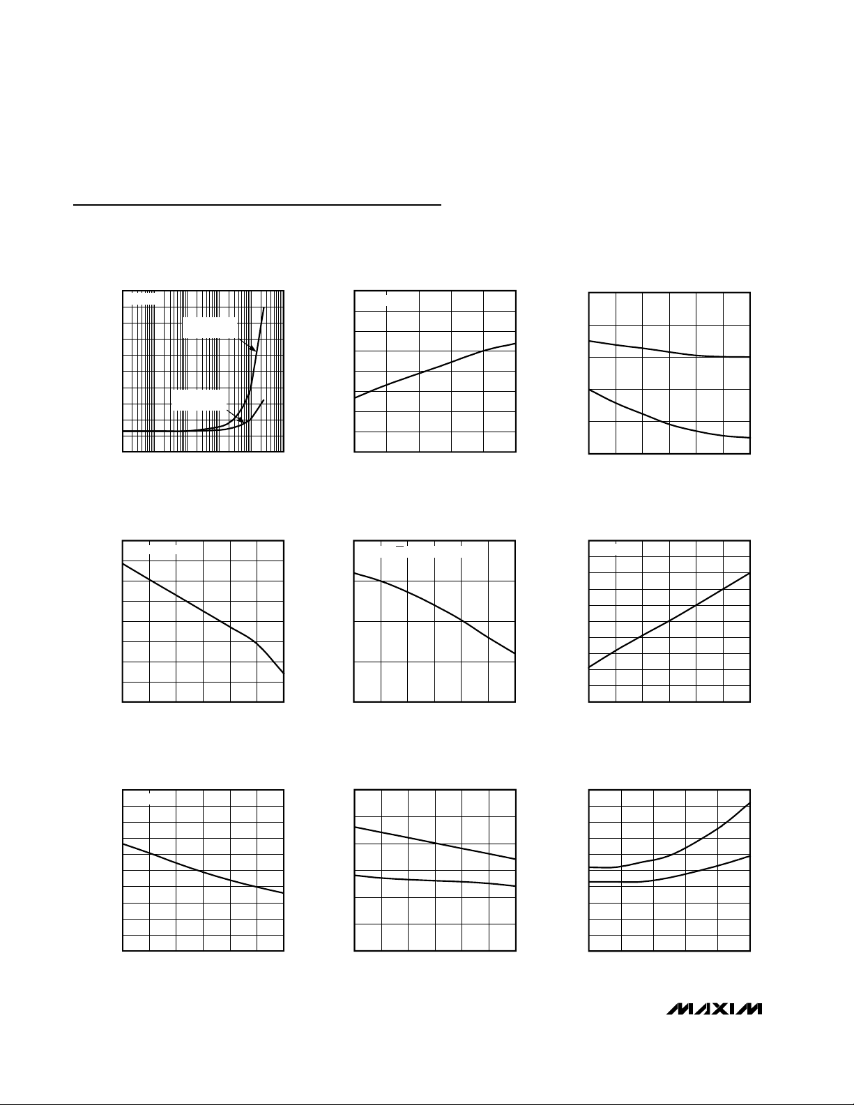
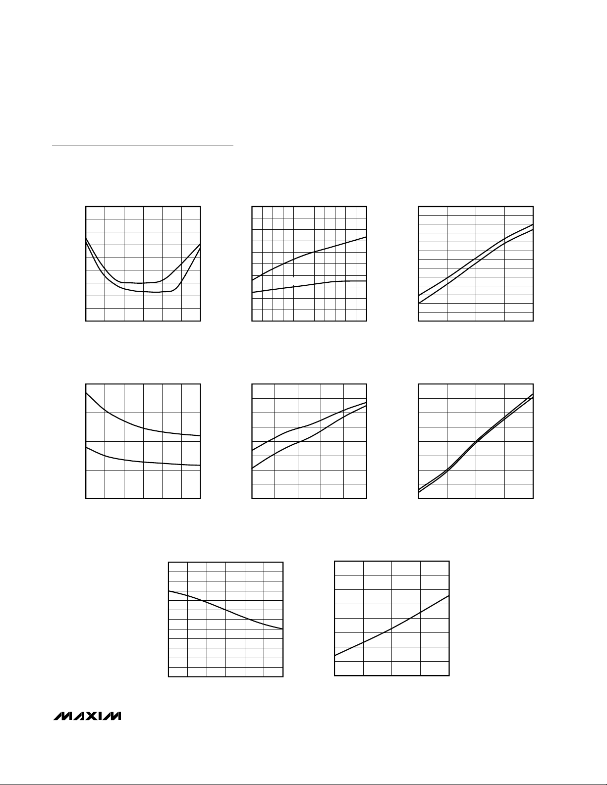
Typical Operating Characteristics
(VCC= 3.3V, VCM= 1.2V, |VID| = 0.2V, f = 100MHz, input rise and fall time = 1ns (0% to 100%), CL= 15pF, and TA= +25°C, unless
otherwise noted.) (Figures 2 and 3)
SUPPLY CURRENT vs. FREQUENCY
MAX9173 toc01
FREQUENCY (MHz)
SUPPLY CURRENT (mA)
1001010.1
10
20
30
40
50
60
70
80
90
100
0
0.01 1000
CL = 15pF
ALL CHANNELS
SWITCHING
ONE CHANNEL
SWITCHING
SUPPLY CURRENT vs. TEMPERATURE
MAX9173 toc02
TEMPERATURE (°C)
SUPPLY CURRENT (mA)
6035-15 10
9
10
11
12
13
14
15
16
8
-40 85
ALL INPUTS OPEN
DIFFERENTIAL THRESHOLD VOLTAGE
vs. SUPPLY VOLTAGE
MAX9173 toc03
SUPPLY VOLTAGE (V)
DIFFERENTIAL INPUT THRESHOLD VOLTAGE (mV)
3.53.43.33.23.1
-51
-47
-43
-39
-35
-55
3.0 3.6
V
TH
V
TL
OUTPUT SHORT-CIRCUIT CURRENT
vs. SUPPLY VOLTAGE
MAX9173 toc04
SUPPLY VOLTAGE (V)
OUTPUT SHORT-CIRCUIT CURRENT (mA)
3.53.43.1 3.2 3.3
-95
-90
-85
-80
-75
-70
-65
-60
-100
3.0 3.6
ALL INPUTS OPEN
OUTPUT HIGH-IMPEDANCE CURRENT
vs. SUPPLY VOLTAGE
MAX9173 toc05
SUPPLY VOLTAGE (V)
OUTPUT HIGH-IMPEDANCE CURRENT (nA)
3.53.43.33.23.1
-0.025
-0.020
-0.015
-0.010
-0.030
3.0 3.6
EN = LOW, EN = HIGH, V
OUT
= 0
OUTPUT HIGH VOLTAGE
vs. SUPPLY VOLTAGE
MAX9173 toc06
SUPPLY VOLTAGE (V)
OUTPUT HIGH VOLTAGE (V)
3.53.43.33.23.1
2.8
2.9
3.0
3.1
3.2
3.3
3.4
3.5
3.6
3.7
2.7
3.0 3.6
IOH = -4mA
OUTPUT LOW VOLTAGE
vs. SUPPLY VOLTAGE
MAX9173 toc07
SUPPLY VOLTAGE (V)
OUTPUT LOW VOLTAGE (mV)
3.53.43.33.23.1
89
90
91
92
93
94
95
96
97
98
88
3.0 3.6
IOL = 4mA
DIFFERENTIAL PROPAGATION DELAY
vs. SUPPLY VOLTAGE
MAX9173 toc08
SUPPLY VOLTAGE (V)
DIFFERENTIAL PROPAGATION DELAY (ns)
3.53.43.33.23.1
1.95
2.00
2.05
2.10
2.15
2.20
1.90
3.0 3.6
t
PLHD
t
PHLD
DIFFERENTIAL PROPAGATION DELAY
vs. TEMPERATURE
MAX9173 toc09
TEMPERATURE (°C)
DIFFERENTIAL PROPAGATION DELAY (ns)
603510-15
1.85
1.90
1.95
2.00
2.05
2.10
2.15
2.20
2.25
2.30
1.80
-40 85
t
PLHD
t
PHLD
Page 5
MAX9173
Quad LVDS Line Receiver with Flow-Through
Pinout and “In-Path” Fail-Safe
_______________________________________________________________________________________ 5
Typical Operating Characteristics (continued)
(VCC= 3.3V, VCM= 1.2V, |VID| = 0.2V, f = 100MHz, input rise and fall time = 1ns (0% to 100%), CL= 15pF, and TA= +25°C, unless
otherwise noted.) (Figures 2 and 3)
DIFFERENTIAL PROPAGATION DELAY
vs. COMMON-MODE VOLTAGE
2.7
2.6
2.5
2.4
2.3
2.2
2.1
2.0
DIFFERENTIAL PROPAGATION DELAY (ns)
1.9
1.8
t
PHLD
0.1 3.1
COMMON-MODE VOLTAGE (V)
TRANSITION TIME vs. SUPPLY VOLTAGE
720
680
640
TRANSITION TIME (ps)
600
560
3.0 3.6
t
TLH
t
THL
SUPPLY VOLTAGE (V)
t
PLHD
DIFFERENTIAL PROPAGATION DELAY
vs. DIFFERENTIAL INPUT VOLTAGE
2.40
MAX9173 toc10
2.62.11.61.10.6
2.35
2.30
2.25
2.20
2.15
2.10
2.05
2.00
DIFFERENTIAL PROPAGATION DELAY (ns)
1.95
1.90
0.1
DIFFERENTIAL INPUT VOLTAGE (V)
t
PHLD
t
PLHD
MAX9173 toc11
1.10.90.3 0.5 0.7
TRANSITION TIME vs. TEMPERATURE
800
MAX9173 toc13
3.53.43.33.23.1
750
700
650
600
550
TRANSITION TIME (ps)
500
450
400
-40 85
t
TLH
t
TEMPERATURE (°C)
THL
MAX9173 toc14
6035-15 10
DIFFERENTIAL PROPAGATION DELAY
vs. LOAD
3.0
2.9
2.8
2.7
2.6
2.5
2.4
2.3
2.2
2.1
2.0
1.9
DIFFERENTIAL PROPAGATION DELAY (ns)
1.8
1.7
10 50
t
PLHD
LOAD (pF)
t
PHLD
TRANSITION TIME vs. LOAD
2000
1800
1600
1400
1200
1000
TRANSITION TIME (ps)
800
600
400
10 50
LOAD (pF)
t
THL
403020
t
TLH
403020
MAX9173 toc12
MAX9173 toc15
DIFFERENTIAL PULSE SKEW
vs. SUPPLY VOLTAGE
120
110
100
90
80
70
60
50
40
30
DIFFERENTIAL PULSE SKEW (ps)
20
10
0
3.0 3.6
SUPPLY VOLTAGE (V)
400
MAX9173 toc16
3.53.43.33.23.1
350
300
250
200
150
100
DIFFERENTIAL PULSE SKEW (ps)
DIFFERENTIAL PULSE SKEW
vs. INPUT TRANSITION TIME
f = 50MHz
50
0
1.0 3.0
INPUT TRANSITION TIME (ns)
2.52.01.5
MAX9173 toc17
Page 6
MAX9173
Detailed Description
LVDS is a signaling method intended for point-to-point
communication over a controlled-impedance medium
as defined by the ANSI TIA/EIA-644 and IEEE 1596.3
standards. LVDS uses a lower voltage swing than other
common communication standards, achieving higher
data rates with reduced power consumption while
reducing EMI and system susceptibility to noise.
The MAX9173 is a 500Mbps, four-channel LVDS receiver intended for high-speed, point-to-point, low-power
applications. Each channel accepts an LVDS input and
translates it to an LVTTL/LVCMOS output. The receiver
is specified to detect differential signals as low as
100mV and as high as 1.2V within an input voltage
range of 0 to VCC. The 250mV to 400mV differential output of an LVDS driver is nominally centered around a
1.2V offset. This offset, coupled with the receiver’s 0 to
VCCinput voltage range, allows more than ±1V shift in
the signal (as seen by the receiver). This allows for a
difference in ground references of the transmitter and
the receiver, the common-mode effects of coupled
noise, or both.
Quad LVDS Line Receiver with Flow-Through
Pinout and “In-Path” Fail-Safe
6 _______________________________________________________________________________________
Pin Description
Table 1. Input/Output Function Table
PIN
TSSOP/SO QFN
1 15 IN1- Inverting Differential Receiver Input for Receiver 1
2 16 IN1+ Noninverting Differential Receiver Input for Receiver 1
3 1 IN2+ Noninverting Differential Receiver Input for Receiver 2
4 2 IN2- Inverting Differential Receiver Input for Receiver 2
5 3 IN3- Inverting Differential Receiver Input for Receiver 3
6 4 IN3+ Noninverting Differential Receiver Input for Receiver 3
7 5 IN4+ Noninverting Differential Receiver Input for Receiver 4
8 6 IN4- Inverting Differential Receiver Input for Receiver 4
9, 16 7, 14 EN, EN
10 8 OUT4 LVCMOS/LVTTL Receiver Output for Receiver 4
11 9 OUT3 LVCMOS/LVTTL Receiver Output for Receiver 3
12 10 GND Ground
13 11 V
14 12 OUT2 LVCMOS/LVTTL Receiver Output for Receiver 2
15 13 OUT1 LVCMOS/LVTTL Receiver Output for Receiver 1
— Exposed Pad EP Exposed Pad. Solder to ground plane for proper heat dissipation.
NAME FUNCTION
Receiver Enable Inputs. When EN = high and EN = low or open, the outputs are active.
For other combinations of EN and EN, the outputs are disabled and in high
impedance.
CC
Power-Supply Input. Bypass VCC to GND with 0.1µF and 0.001µF ceramic capacitors.
Place the smaller value cap as close to the pin as possible.
EN EN (IN_+) - (IN_-) OUT_
All other combinations of ENABLE pins Don’t care Z
ENABLES INPUTS OUTPUT
VID ≥ 0H
H L or open
Open, undriven short, or undriven parallel termination H
VID ≤ -100mV L
Page 7
Fail-Safe
The MAX9173 fail-safe drives the receiver output high
when the differential input is:
• Open
• Undriven and shorted
• Undriven and terminated
Without fail-safe, differential noise at the input may
switch the receiver and appear as data to the receiving
system. An open input occurs when a cable and termination are disconnected. An undriven, terminated input
occurs when a cable is disconnected with the termination still connected across the receiver inputs or when
the driver of a receiver is in high impedance. An undriven, shorted input can occur due to a shorted cable.
“In-Path” vs. “Parallel” Fail-Safe
The MAX9173 has in-path fail-safe that is compatible
with in-path fail-safe receivers, such as the
DS90LV048A. Refer to the MAX9121/MAX9122 data
sheet for pin-compatible receivers with parallel fail-safe
and lower jitter. Refer to the MAX9130 data sheet for a
single LVDS receiver with parallel fail-safe in an SC70
package.
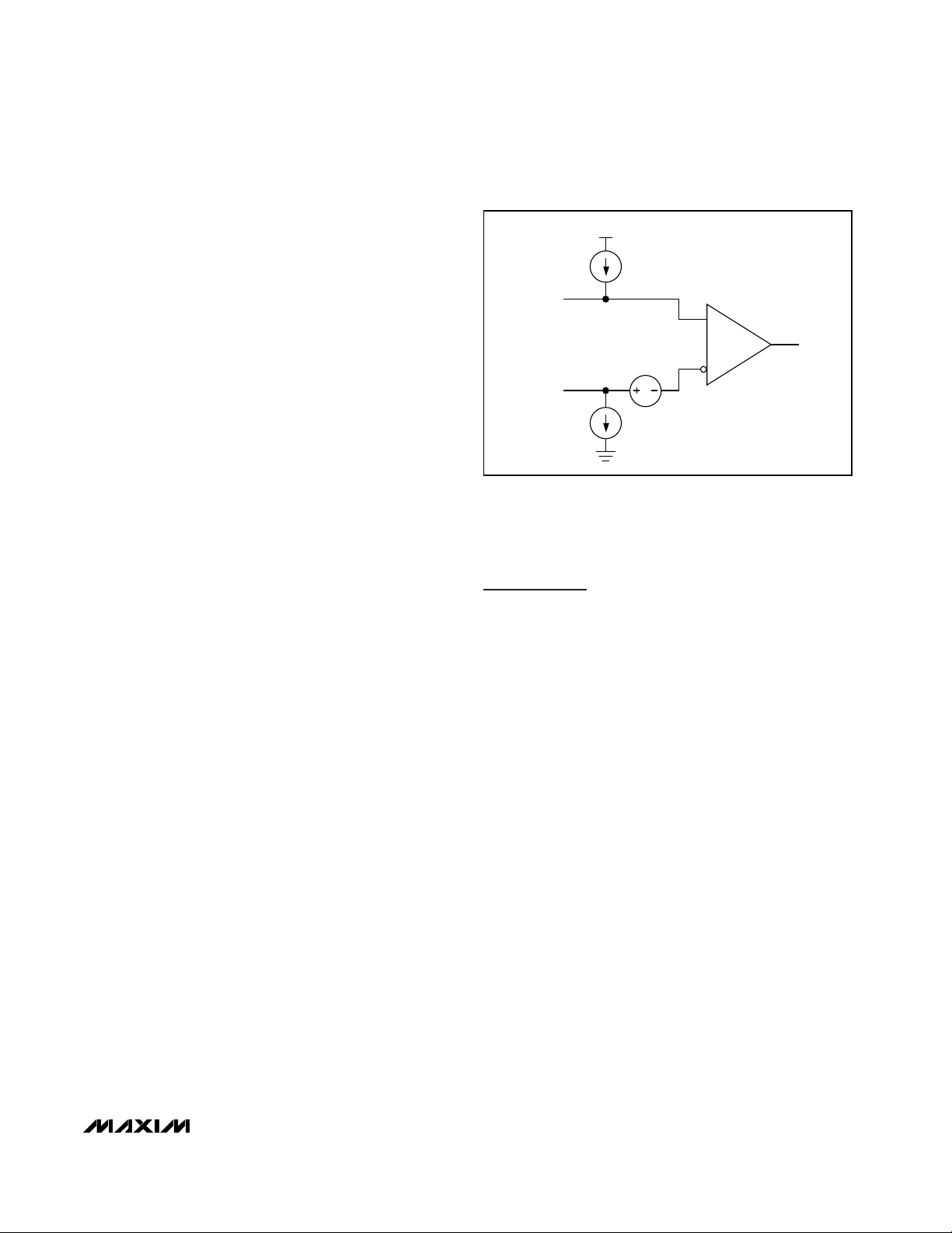
The MAX9173 with in-path fail-safe is designed with a
+45mV input offset voltage, a 2.5µA current source
between VCCand the noninverting input, and a 5µA
current sink between the inverting input and ground
(Figure 1). If the differential input is open, the 2.5µA
current source pulls the input to approximately VCC-
0.8V and the 5µA current sink pulls the inverting input
to ground, which drives the receiver output high. If the
differential input is shorted or terminated with a typical
value termination resistor, the +45mV offset drives the
receiver output high. If the input is terminated and floating, the receiver output is driven high by the +45mV offset, and the 2:1 current sink to current source ratio
(5µA:2.5µA) pulls the inputs to ground. This can be an
advantage when switching between drivers on a multipoint bus because the change in common-mode voltage from ground to the typical driver offset voltage of
1.2V is not as much as the change from VCCto 1.2V
(parallel fail-safe pulls the bus to VCC).
ESD Protection
ESD-protection structures are incorporated on all pins
to protect against electrostatic discharges encountered
during handling and assembly. The receiver inputs of
the MAX9173 have ±7.0kV of protection against static
electricity (per Human Body Model).
Figure 6a shows the Human Body Model, and Figure
6b shows the current waveform it generates when discharged into a low-impedance load. This model con-
sists of a 100pF capacitor charged to the ESD test voltage, which is then discharged into the test device
through a 1.5kΩ resistor.
Applications Information
Differential Traces
Input trace characteristics affect the performance of the
MAX9173. Use controlled-impedance board traces. For
point-to-point connections, match the receiver input termination resistor to the differential characteristic impedance of the board traces.
Eliminate reflections and ensure that noise couples as
common mode by running the differential traces close
together. Reduce skew by matching the electrical
length of the traces. Excessive skew can result in a
degradation of magnetic field cancellation.
Each channel’s differential signals should be routed
close to each other to cancel their external magnetic
field. Maintain a constant distance between the differential traces to avoid discontinuities in differential
impedance. Minimize the number of vias to further prevent impedance discontinuities.
Cables and Connectors
LVDS transmission media typically have controlled differential impedance of 100Ω. Use cables and connectors that have matched differential impedance to
minimize impedance discontinuities.
Avoid the use of unbalanced cables such as coaxial
cable. Balanced cables such as twisted pair offer
superior signal quality and tend to generate less EMI
due to magnetic field canceling effects. Balanced
cables pick up noise as common mode, which is rejected by the LVDS receiver.
MAX9173
Quad LVDS Line Receiver with Flow-Through
Pinout and “In-Path” Fail-Safe
_______________________________________________________________________________________ 7
Figure 1. Input with Fail-Safe Network
V
CC
2.5µA
IN_+
OUT_
IN_-
45mV
5µA
Page 8

MAX9173
Termination
The MAX9173 requires an external termination resistor.
The termination resistor should match the differential
impedance of the transmission line. Termination resistance values may range between 90Ω to 132Ω,
depending on the characteristic impedance of the
transmission medium.
When using the MAX9173, minimize the distance between the input termination resistors and the MAX9173
receiver inputs. Use 1% surface-mount resistors.
Board Layout
In general, separate the LVDS inputs from single-ended
outputs to reduce crosstalk. Take special care when
routing traces with the QFN package. Ideally, the LVDS
inputs should be separated by 180° from the
LVTTL/LVCMOS outputs to reduce crosstalk.
For LVDS applications, a four-layer PC board that provides separate layers of power, ground, LVDS inputs, and
output signals is recommended. When using the QFN
package, solder the exposed pad (EP) to the ground
plane using an array of vias for proper heat dissipation.
Chip Information
TRANSISTOR COUNT: 1462
PROCESS: CMOS
Quad LVDS Line Receiver with Flow-Through
Pinout and “In-Path” Fail-Safe
8 _______________________________________________________________________________________
Figure 2. Propagation Delay and Transition Time Test Circuit
Figure 3. Propagation Delay and Transition Time Test Waveforms
PULSE
GENERATOR
*50Ω REQUIRED FOR PULSE GENERATOR.
50Ω*
IN_+
OUT_
C
IN_-
50Ω*
L
IN_-
= 0.2V
t
PHLD
80%
1.5V
V
ID
20%
t
THL
1.2V (0V DIFFERENTIAL)
IN_+
t
PLHD
80%
1.5V
20%
OUT_
t
TLH
1.3V
1.1V
V
OH
V
OL
Page 9
MAX9173
Quad LVDS Line Receiver with Flow-Through
Pinout and “In-Path” Fail-Safe
_______________________________________________________________________________________ 9
Figure 4. High-Impedance Delay Test Circuit
Figure 5. High-Impedance Delay Waveforms
Figure 6a. Human Body ESD Test Modules Figure 6b. Human Body Current Waveform
GENERATOR
INCLUDES LOAD AND TEST JIG CAPACITANCE.
C
L
= VCC FOR t
S
1
= GND FOR t
S
1
PZL
PZH
AND t
AND t
MEASUREMENTS.
PLZ
MEASUREMENTS.
PHZ
EN WHEN EN = GND OR OPEN
1.5V
1.5V
EN WHEN EN = V
OUTPUT WHEN
OUTPUT WHEN
= -100mV
V
ID
CC
t
t
PHZ
= 0
V
ID
50Ω
V
CC
IN_+
DEVICE
UNDER
EN
EN
1/4 MAX9173
IN_-
TEST
S
1
R
L
OUT_
C
L
3V
1.5V
0
3V
1.5V
0
t
PZL
PLZ
50%
0.5V
t
PZH
0.5V
V
CC
V
OL
V
OH
50%
GND
1M RD 1500Ω
R
C
HIGH-
VOLTAGE
DC
SOURCE
CHARGE-CURRENT
LIMIT RESISTOR
C
100pF
AMPERES
IP 100%
90%
36.8%
10%
0
0
t
RL
DISCHARGE
RESISTANCE
STORAGE
s
CAPACITOR
DEVICE
UNDER
TEST
I
r
TIME
t
DL
CURRENT WAVEFORM
PEAK-TO-PEAK RINGING
(NOT DRAWN TO SCALE)
Page 10

MAX9173
Quad LVDS Line Receiver with Flow-Through
Pinout and “In-Path” Fail-Safe
10 ______________________________________________________________________________________
Functional Diagram
TOP VIEW
TSSOP/SO
16
15
14
13
12
11
10
9
1
2
3
4
5
6
7
8
IN1-
EN
OUT1
OUT2
V
CC
GND
OUT3
OUT4
EN
MAX9173
IN1+
IN2+
IN3+
IN2-
IN3-
IN4+
IN4-
16
15
14
13
IN1+
IN1-ENOUT1
9
10
11
12
OUT3
GND
V
CC
OUT2
4
3
2
1
IN3+
IN3-
IN2-
IN2+
5
6
7
8
IN4+
IN4-
EN
OUT4
MAX9173
THIN QFN-EP
Pin Configurations
V
CC
IN1+
OUT1
IN1-
IN2+
OUT2
IN2-
IN3+
OUT3
IN3-
IN4+
OUT4
IN4-
EN
EN
GND
MAX9173
Page 11

MAX9173
Quad LVDS Line Receiver with Flow-Through
Pinout and “In-Path” Fail-Safe
______________________________________________________________________________________ 11
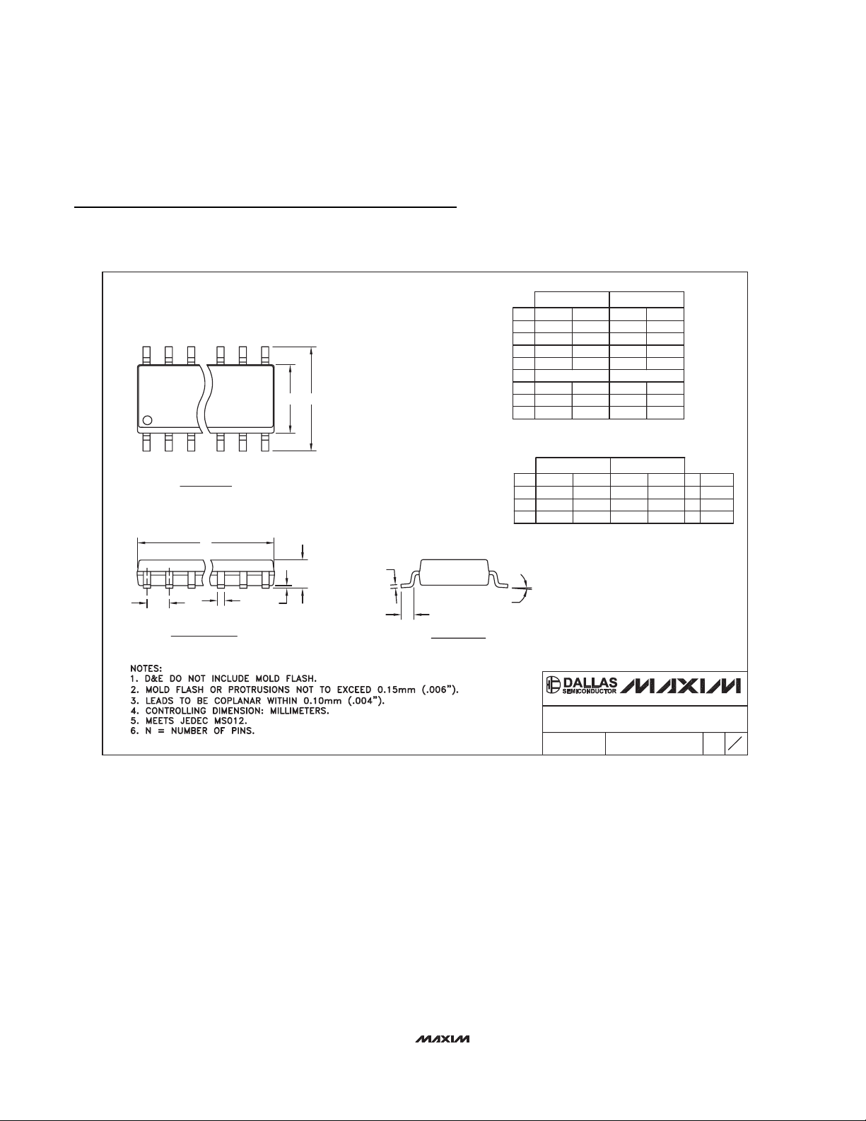
Package Information
(The package drawing(s) in this data sheet may not reflect the most current specifications. For the latest package outline information,
go to www.maxim-ic.com/packages.)
TSSOP4.40mm.EPS
Page 12

MAX9173
Quad LVDS Line Receiver with Flow-Through
Pinout and “In-Path” Fail-Safe
12 ______________________________________________________________________________________
Package Information (continued)
(The package drawing(s) in this data sheet may not reflect the most current specifications. For the latest package outline information,
go to www.maxim-ic.com/packages.)
D2
b
D
D/2
D2/2
0.10 M C A B
E/2
- A -
C
L
E
(NE - 1) X e
E2/2
E2
12x16L QFN THIN.EPS
0.10
- B -
C
L
C
C
0.08
C
A
A2
A1
L
L
e
e
PROPRIETARY INFORMATION
TITLE:
PACKAGE OUTLINE
12 & 16L, QFN THIN, 3x3x0.8 mm
k
(ND - 1) X e
C
L
e
21-0136
L
L
REV.DOCUMENT CONTROL NO.APPROVAL
1
C
2
Page 13

MAX9173
Quad LVDS Line Receiver with Flow-Through
Pinout and “In-Path” Fail-Safe
______________________________________________________________________________________ 13
Package Information (continued)
(The package drawing(s) in this data sheet may not reflect the most current specifications. For the latest package outline information,
go to www.maxim-ic.com/packages.)
EXPOSED PAD VARIATIONS
NOTES:
1. DIMENSIONING & TOLERANCING CONFORM TO ASME Y14.5M-1994.
2. ALL DIMENSIONS ARE IN MILLIMETERS. ANGLES ARE IN DEGREES.
3. N IS THE TOTAL NUMBER OF TERMINALS.
4. THE TERMINAL #1 IDENTIFIER AND TERMINAL NUMBERING CONVENTION SHALL CONFORM TO
JESD 95-1 SPP-012. DETAILS OF TERMINAL #1 IDENTIFIER ARE OPTIONAL, BUT MUST BE LOCATED
WITHIN THE ZONE INDICATED. THE TERMINAL #1 IDENTIFIER MAY BE EITHER A MOLD OR
MARKED FEATURE.
5. DIMENSION b APPLIES TO METALLIZED TERMINAL AND IS MEASURED BETWEEN 0.20 mm AND 0.25 mm
FROM TERMINAL TIP.
6. ND AND NE REFER TO THE NUMBER OF TERMINALS ON EACH D AND E SIDE RESPECTIVELY.
7. DEPOPULATION IS POSSIBLE IN A SYMMETRICAL FASHION.
8. COPLANARITY APPLIES TO THE EXPOSED HEAT SINK SLUG AS WELL AS THE TERMINALS.
9. DRAWING CONFORMS TO JEDEC MO220 REVISION C.
PROPRIETARY INFORMATION
TITLE:
PACKAGE OUTLINE
12 & 16L, QFN THIN, 3x3x0.8 mm
APPROVAL
DOCUMENT CONTROL NO.
21-0136
REV.
2
C
2
Page 14
MAX9173
Quad LVDS Line Receiver with Flow-Through
Pinout and “In-Path” Fail-Safe
Maxim cannot assume responsibility for use of any circuitry other than circuitry entirely embodied in a Maxim product. No circuit patent licenses are
implied. Maxim reserves the right to change the circuitry and specifications without notice at any time.
14 ____________________Maxim Integrated Products, 120 San Gabriel Drive, Sunnyvale, CA 94086 408-737-7600
© 2002 Maxim Integrated Products Printed USA is a registered trademark of Maxim Integrated Products.
Package Information (continued)
(The package drawing(s) in this data sheet may not reflect the most current specifications. For the latest package outline information,
go to www.maxim-ic.com/packages.)
N
1
e
FRONT VIEW
TOP VIEW
D
INCHES
DIM
MIN
0.053A
0.004
A1
0.014
B
0.007
C
e 0.050 BSC 1.27 BSC
0.150
HE
A
B
A1
C
L
E
H 0.2440.228 5.80 6.20
0.016L
VARIATIONS:
INCHES
MINDIM
D
0.189 0.197 AA5.004.80 8
0.337 0.344 AB8.758.55 14
D
0-8
MAX
0.069
0.010
0.019
0.010
0.157
0.050
MAX
0.3940.386D
MILLIMETERS
MAX
MIN
1.35
1.75
0.10
0.25
0.35
0.49
0.19
0.25
3.80 4.00
0.40 1.27
MILLIMETERS
MAX
MIN
9.80 10.00
N MS012
16
AC
SOICN .EPS
SIDE VIEW
PROPRIETARY INFORMATION
TITLE:
PACKAGE OUTLINE, .150" SOIC
REV.DOCUMENT CONTROL NO.APPROVAL
21-0041
1
B
1
 Loading...