

Page 1
General Description
The MAX9171/MAX9172 single/dual low-voltage differential
signaling (LVDS) receivers are designed for high-speed
applications requiring minimum power consumption,
space, and noise. Both devices support switching rates
exceeding 500Mbps while operating from a single 3.3V
supply.
The MAX9171 is a single LVDS receiver and the
MAX9172 is a dual LVDS receiver. Both devices conform to the ANSI TIA/EIA-644 LVDS standard and convert LVDS to LVTTL/LVCMOS-compatible outputs. A
fail-safe feature sets the outputs high when the inputs
are undriven and open, terminated, or shorted. The
MAX9171/MAX9172 are available in 8-pin SO packages
and space-saving thin DFN and SOT23 packages.
For lower skew devices, refer to the MAX9111/ MAX9113
data sheet.
Applications
Multipoint Backplane Interconnect
Laser Printers
Digital Copiers
Cellular Phone Base Stations
LCD Displays
Network Switches/Routers
Clock Distribution
Features
♦ Input Accepts LVDS and LVPECL
♦ In-Path Fail-Safe Circuit
♦ Space-Saving 8-Pin TDFN and SOT23 Packages
♦ Fail-Safe Circuitry Sets Output High for Open,
Undriven Shorted, or Undriven Terminated Output
♦ Flow-Through Pinout Simplifies PCB Layout
♦ Guaranteed 500Mbps Data Rate
♦ Second Source to DS90LV018A and DS90LV028A
(SO Packages Only)
♦ Conforms to ANSI TIA/EIA-644 Standard
♦ 3.3V Supply Voltage
♦ -40°C to +85°C Operating Temperature Range
♦ Low-Power Dissipation
MAX9171/MAX9172
Single/Dual LVDS Line Receivers with
“In-Path” Fail-Safe
________________________________________________________________ Maxim Integrated Products 1
Ordering Information
19-2578; Rev 2; 6/07
For pricing, delivery, and ordering information, please contact Maxim Direct at 1-888-629-4642,
or visit Maxim’s website at www.maxim-ic.com.
PART PIN-PACKAGE
TOP
PKG
CODE
MAX9171EKA-T
8 SOT23-8 AALX K8-1
MAX9171ESA 8 SO — S8-2
MAX9171ETA*
—
T833-2
MAX9172EKA-T
8 SOT23-8 AALY K8-1
MAX9172ESA 8 SO — S8-2
MAX9172ETA*
—
T833-2
1
2
3
4
5
6
7
8
SO/TDFN*
IN-
IN+
N.C.
N.C.
GND
N.C.
OUT
V
CC
IN-
IN+
N.C.
N.C.
GND
N.C.
OUT
V
CC
IN1-
IN1+
IN2+
IN2-
GND
OUT2
OUT1
V
CC
IN1-
IN1+
IN2-
OUT2
GND
IN2+
OUT1
V
CC
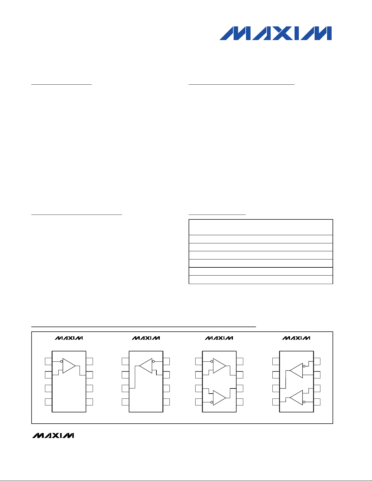
MAX9171
1
2
3
4
5
6
7
8
SO/TDFN*
MAX9172
1
2
3
4
5
6
7
8
SOT23
MAX9172
1
2
3
4
8
7
6
5
SOT23
MAX9171
Pin Configurations
Note: All devices are specified over the -40°C to +85°C operating
temperature range.
*Future product—contact factory for availability.
**EP = Exposed pad.
T = Tape-and-reel.
MARK
8 Thin DFN-EP**
8 Thin DFN-EP**
Page 2
MAX9171/MAX9172
Single/Dual LVDS Line Receivers with
“In-Path” Fail-Safe
2 _______________________________________________________________________________________
ABSOLUTE MAXIMUM RATINGS
ELECTRICAL CHARACTERISTICS
(VCC= 3.0V to 3.6V, differential input voltage |VID| = 0.1V to 1.2V, receiver input voltage = 0 to VCC, common-mode voltage VCM=
|V
ID
/2| to (VCC- |VID/2|), TA= -40°C to +85°C, unless otherwise noted. Typical values are at VCC= 3.3V, |VID| = 0.2V, VCM= 1.2V,
T
A
= +25°C.) (Notes 1, 2)
Stresses beyond those listed under “Absolute Maximum Ratings” may cause permanent damage to the device. These are stress ratings only, and functional
operation of the device at these or any other conditions beyond those indicated in the operational sections of the specifications is not implied. Exposure to
absolute maximum rating conditions for extended periods may affect device reliability.
VCCto GND...........................................................-0.3V to +4.0V
IN_+, IN_- to GND .................................................-0.3V to +4.0V
OUT_ to GND ............................................-0.3V to (VCC+ 0.3V)
Continuous Power Dissipation (TA= +70°C)
8-Pin SOT23 (derate 8.9mW/°C above +70°C) ...........714mW
8-Pin SO (derate 5.9mW/°C above +70°C) .................471mW
8-Pin TDFN (derate 24.4mW/°C above +70°C) ........1951mW
Operating Temperature Range ..........................-40°C to +85°C
Junction Temperature .....................................................+150°C
Storage Temperature Range ............................-65°C to +150°C
ESD Protection
Human Body Model (IN_+, IN_-) ...................................±13kV
Lead Temperature (soldering, 10s) ................................+300°C
PARAMETER
CONDITIONS
UNITS
LVDS INPUTS (IN_+, IN_-)
Differential Input High Threshold
V
TH
Figure 1 -40 0 mV
Differential Input Low Threshold V
TL
Figure 1
-40 mV
Input Current (Noninverting Input)
I
IN+
Figure 1
µA
Power-Off Input Current
(Noninverting Input)
V
IN+
= 0 to 3.6V, V
IN-
= 0 to 3.6V, VCC = 0
or open (Figure 1)
0
µA
Input Current (Inverting Input) I
IN-
Figure 1
µA
Power-Off Input Current
(Inverting Input)
I
IN-OFF
V
IN+
= 0 to 3.6V, V
IN-
= 0 to 3.6V, VCC = 0
or open (Figure 1)
0
µA
LVCMOS/LVTTL OUTPUTS (OUT_)
Open, undriven short, or
2.7 3.2
Output High Voltage V
OH
VID = 0V 2.7 3.2
V
Output Low Voltage V
OL
IOL = 4.0mA, VID = -100mV 0.1 0.4 V
Output Short-Circuit Current I
OS
V
OUT_
= 0 (Note 3) -45 -77
mA
POWER SUPPLY
MAX9171 3.6 6
Supply Current I
CC
MAX9172 7.0 9
mA
SYMBOL
MIN TYP MAX
-100
+0.5 -2.1 -5.0
I
IN+OFF
IOH = -4.0mA
Inputs open
undriven parallel termination
-0.5
-0.5 +4.4 +10.0
-0.5
+0.5
+0.5
-120
Page 3
MAX9171/MAX9172
Single/Dual LVDS Line Receivers with
“In-Path” Fail-Safe
_______________________________________________________________________________________ 3
Note 1: Current into a pin is defined as positive. Current out of a pin is defined as negative. All voltages are referenced to GND
except V
TH
, VTL, and VID.
Note 2: All devices are 100% production tested at TA= +25°C and are guaranteed by design for TA= -40°C to +85°C, as specified.
Note 3: Short only one output at a time. Do not exceed the absolute maximum junction temperature specification.
Note 4: AC parameters are guaranteed by design and not production tested.
Note 5: C
L
includes scope probe and test jig capacitance.
Note 6: Pulse generator output conditions: t
R
= tF< 1ns (0% to 100%), frequency = 250MHz, 50% duty cycle, VOH= 1.3V, VOL= 1.1V.
Note 7: t
SKD1
is the magnitude of the difference of differential propagation delays in a channel. t
SKD1
= |t
PHLD
- t
PLHD
|.
Note 8: t
SKD2
is the magnitude of the difference of the t
PLHD
or t
PHLD
of one channel and the t
PLHD
or t
PHLD
of the other channel on
the same part.
Note 9: t
SKD3
is the magnitude of the difference of any differential propagation delays between parts at the same VCCand within
5°C of each other.
Note 10: t
SKD4
is the magnitude of the difference of any differential propagation delays between parts operating over the rated
supply and temperature ranges.
SWITCHING CHARACTERISTICS
(VCC= 3.0V to 3.6V, CL= 15pF, |VID| = 0.2V, VCM= 1.2V, TA= -40°C to +85°C, unless otherwise noted. Typical values are at VCC=
3.3V, T
A
= +25°C.) (Notes 4, 5, 6)
PARAMETER
CONDITIONS
UNITS
Differential Propagation Delay
High to Low
t
PHLD
Figures 2, 3 1.0
2.5 ns
Differential Propagation Delay
Low to High
t
PLHD
Figures 2, 3 1.0
2.5 ns
Differential Pulse Skew
|t
PHLD
- t
PLHD
|
t
SKD1
Figures 2, 3 (Note 7) 30 400 ps
Differential Channel-to-Channel
Skew (MAX9172)
t
SKD2
Figures 2, 3 (Note 8) 40 500 ps
t
SKD3
Figures 2, 3 (Note 9) 1
Differential Part-to-Part Skew
t
SKD4
Figures 2, 3 (Note 10) 1.5
ns
Rise Time t
TLH
Figures 2, 3
0.8 ns
Fall Time t
THL
Figures 2, 3
0.8 ns
Maximum Operating Frequency f
MAX
All channels switching, V
OL(MAX)
= 0.4V,
V
OH(MIN)
= 2.7V, 40% < duty cycle < 60%
MHz
SYMBOL
MIN TYP MAX
1.65
1.62
0.55
0.51
250 300
Page 4
MAX9171/MAX9172
Single/Dual LVDS Line Receivers with
“In-Path” Fail-Safe
4 _______________________________________________________________________________________
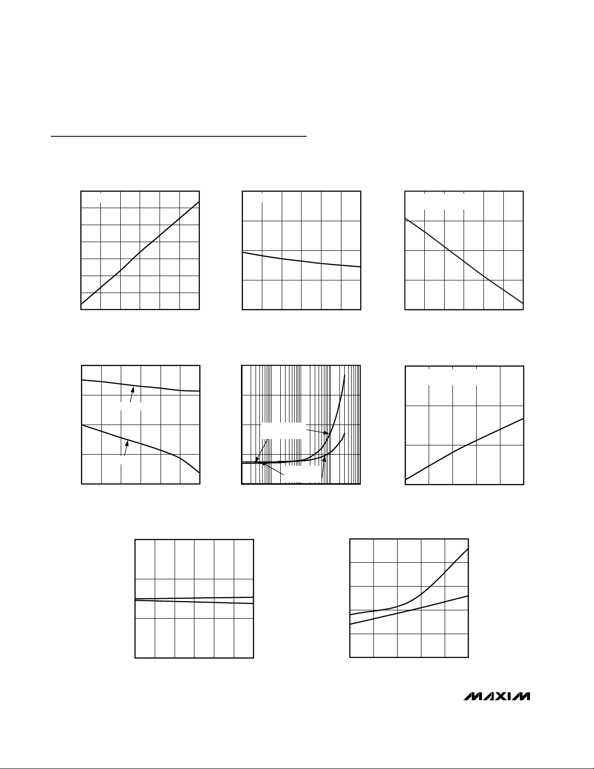
Typical Operating Characteristics
(VCC= 3.3V, VCM= 1.2V, |VID| = 0.2V, fIN= 200MHz, CL= 15pF, TA= +25°C, unless otherwise specified.)
OUTPUT HIGH VOLTAGE
vs. SUPPLY VOLTAGE
MAX9171 toc01
SUPPLY VOLTAGE (V)
OUTPUT HIGH VOLTAGE (V)
3.53.43.33.23.1
3.0
3.1
3.2
3.3
3.4
3.5
3.6
2.9
3.0 3.6
IOH = -4mA
OUTPUT LOW VOLTAGE
vs. SUPPLY VOLTAGE
MAX9171 toc02
SUPPLY VOLTAGE (V)
OUTPUT LOW VOLTAGE (mV)
3.53.43.33.23.1
85
90
95
100
80
3.0 3.6
IOL = +4mA
OUTPUT SHORT-CIRCUIT CURRENT
vs. SUPPLY VOLTAGE
MAX9171 toc03
SUPPLY VOLTAGE (V)
OUTPUT SHORT-CIRCUIT CURRENT (mA)
3.53.43.33.23.1
-80
-75
-70
-65
-85
3.0 3.6
VID = +200mV, OUTPUT
SHORTED TO GROUND
DIFFERENTIAL THRESHOLD VOLTAGE
vs. SUPPLY VOLTAGE
MAX9171 toc04
SUPPLY VOLTAGE (V)
DIFFERENTIAL THRESHOLD VOLTAGE (mV)
3.53.43.33.23.1
-50
-45
-40
-35
-55
3.0 3.6
HIGH-LOW
LOW-HIGH
MAX9172 SUPPLY CURRENT
vs. FREQUENCY
MAX9171 toc05
FREQUENCY (MHz)
SUPPLY CURRENT (mA)
100101
10
20
30
40
0
0.1 1000
BOTH CHANNELS
SWITCHING
ONE CHANNEL
SWITCHING
MAX9172 SUPPLY CURRENT
vs. TEMPERATURE
MAX9171 toc06
TEMPERATURE (°C)
SUPPLY CURRENT (mA)
603510-15
7
8
9
6
-40 85
f = 1MHz
BOTH CHANNELS SWITCHING
DIFFERENTIAL PROPAGATION DELAY
vs. SUPPLY VOLTAGE
MAX9171 toc07
SUPPLY VOLTAGE (V)
DIFFERENTIAL PROPAGATION DELAY (ns)
3.53.43.33.23.1
1.5
2.0
2.5
1.0
3.0 3.6
t
PHLD
t
PLHD
DIFFERENTIAL PROPAGATION DELAY
vs. TEMPERATURE
MAX9171 toc08
TEMPERATURE (°C)
DIFFERENTIAL PROPAGATION DELAY (ns)
603510-15
1.6
1.7
1.8
1.9
2.0
1.5
-40 85
t
PHLD
t
PLHD
Page 5

MAX9171/MAX9172
Single/Dual LVDS Line Receivers with
“In-Path” Fail-Safe
_______________________________________________________________________________________ 5
DIFFERENTIAL PULSE SKEW
vs. SUPPLY VOLTAGE
MAX9171 toc09
SUPPLY VOLTAGE (V)
DIFFERENTIAL PULSE SKEW (ps)
3.53.43.33.23.1
30
60
90
120
0
3.0 3.6
DIFFERENTIAL PULSE SKEW
vs. TEMPERATURE
MAX9171 toc10
TEMPERATURE (°C)
DIFFERENTIAL PULSE SKEW (ps)
603510-15
40
80
120
160
200
0
-40 85
DIFFERENTIAL PROPAGATION DELAY
vs. DIFFERENTIAL INPUT VOLTAGE
MAX9171 toc11
DIFFERENTIAL INPUT VOLTAGE (mV)
DIFFERENTIAL PROPAGATION DELAY (ns)
210016001100600
1.5
2.0
2.5
3.0
1.0
100 2600
fIN = 20MHz
t
PHLD
t
PLHD
DIFFERENTIAL PROPAGATION DELAY
vs. COMMON-MODE VOLTAGE
MAX9171 toc12
COMMON-MODE VOLTAGE (V)
DIFFERENTIAL PROPAGATION DELAY (ns)
2.62.11.61.10.6
1.3
1.6
1.9
2.2
2.5
1.0
0.1 3.1
fIN = 20MHz
t
PHLD
t
PLHD
TRANSITION TIME vs. TEMPERATURE
MAX9171 toc13
TEMPERATURE (°C)
TRANSITION TIME (ps)
603510-15
400
500
600
700
300
-40 85
t
TLH
t
THL
DIFFERENTIAL PROPAGATION DELAY
vs. LOAD
MAX9171 toc14
LOAD (pF)
DIFFERENTIAL PROPAGATION DELAY (ns)
403020
1.6
1.8
2.0
2.2
2.4
1.4
10 50
fIN = 20MHz
t
PHLD
t
PLHD
TRANSITION TIME vs. LOAD
MAX9171 toc15
LOAD (pF)
TRANSITION TIME (ps)
403020
500
900
1300
1700
2100
100
10 50
t
TLH
t
THL
DIFFERENTIAL PULSE SKEW
vs. INPUT TRANSITION TIME
MAX9171 toc16
INPUT TRANSITION TIME (ns)
DIFFERENTIAL PULSE SKEW (ps)
2.52.01.5
50
100
150
200
250
300
0
1.0 3.0
Typical Operating Characteristics (continued)
(VCC= 3.3V, VCM= 1.2V, |VID| = 0.2V, fIN= 200MHz, CL= 15pF, TA= +25°C, unless otherwise specified.)
Page 6

MAX9171/MAX9172
Detailed Description
LVDS Inputs
The MAX9171/MAX9172 feature LVDS inputs for interfacing high-speed digital circuitry. The LVDS interface
standard is a signaling method intended for point-topoint communication over controlled-impedance
media, as defined by the ANSI TIA/EIA-644 standards.
The technology uses low-voltage signals to achieve fast
transition times and minimize power dissipation and
noise immunity. The MAX9171/MAX9172 convert LVDS
signals to LVCMOS/LVTTL signals at rates in excess of
500Mbps. These devices are capable of detecting differential signals as low as 100mV and as high as 1.2V
within a 0 to VCCinput voltage range. Table 1 is the
input-output function table.
Fail-Safe
The MAX9171/MAX9172 fail-safe drives the receiver
output high when the differential input is:
• Open
• Undriven and shorted
• Undriven and terminated
Without fail-safe, differential noise at the input may
switch the receiver and appear as data to the receiving
system. An open input occurs when a cable and termination are disconnected. An undriven, terminated input
occurs when a cable is disconnected with the termination still connected across the receiver inputs or when
the driver of a receiver is in high impedance. An undriven, shorted input can occur due to a shorted cable.
Single/Dual LVDS Line Receivers with
“In-Path” Fail-Safe
6 _______________________________________________________________________________________
MAX9171 Pin Description
PIN
SOT23
NAME FUNCTION
18V
CC
Positive Power-Supply Input. Bypass with a 0.1µF and a 0.001µF capacitor to GND with the
smallest capacitor closest to the pin.
2 5 GND Ground
3 7 OUT Receiver Output
4, 5, 6 3, 4, 6 N.C. No Connection. Not internally connected.
7 2 IN+ Noninverting Differential Receiver Input
8 1 IN- Inverting Differential Receiver Input
—
EP Exposed Paddle. Solder to PCB ground.
MAX9172 Pin Description
PIN
SOT23
NAME FUNCTION
18V
CC
Positive Power-Supply Input. Bypass with a 0.1µF and a 0.001µF capacitor to GND with the
smallest capacitor closest to the pin.
2 5 GND Ground
3 7 OUT1 Receiver Output 1
4 6 OUT2 Receiver Output 2
5 4 IN2- Inverting Differential Receiver Input 2
6 3 IN2+ Noninverting Differential Receiver Input 2
7 2 IN1+ Noninverting Differential Receiver Input 1
8 1 IN1- Inverting Differential Receiver Input 1
—
EP Exposed Paddle. Solder to PCB ground.
INPUTS OUTPUT
(IN_+) - (IN_-) OUT_
≥ 0mV High
≤ -100mV Low
Open High
Undriven short High
Undriven parallel termination
High
Table 1. Input-Output Function Table
SO/TDFN
( TD FN onl y)
SO/TDFN
( TD FN onl y)
Page 7

In-Path vs. Parallel Fail-Safe
The MAX9171/MAX9172 have in-path fail-safe that is
compatible with in-path fail-safe receivers, such as the
DS90LV018A and DS90LV028A. Refer to the MAX9111/
MAX9113 data sheet for pin-compatible receivers with
parallel fail-safe and lower jitter. Refer to the MAX9130
data sheet for a single LVDS receiver with parallel failsafe in an SC70 package.
The MAX9171/MAX9172 with in-path fail-safe are
designed with a +40mV input offset voltage, a 2.5µA
current source between VCCand the noninverting
input, and a 5µA current sink between the inverting
input and ground (Figure 1). If the differential input is
open, the 2.5µA current source pulls the input to VCC-
0.7V and the 5µA source sink pulls the inverting input to
ground, which drives the receiver output high. If the differential input is shorted or terminated with a typical
value termination resistor, the +40mV offset drives the
receiver output high. If the input is terminated and floating, the receiver output is driven high by the +40mV offset, and the 2:1 current sink to current source ratio
(5µA:2.5µA) pulls the inputs to ground. This can be an
advantage when switching between drivers on a multipoint bus because the change in common-mode voltage from ground to the typical driver offset voltage of
1.2V is not as much as the change from VCCto 1.2V
(parallel fail-safe pulls the bus to VCC). Figure 2 shows
the propagation delay and transition test time circuit
and Figure 3 shows the propagation delay and transition test time waveforms.
MAX9171/MAX9172
Single/Dual LVDS Line Receivers with
“In-Path” Fail-Safe
_______________________________________________________________________________________ 7
OUT_
V
CC
IN_+
IN_-
5µA
2.5µA
40mV
Figure 1. Input with In-Path Fail-Safe Network Equivalent Circuit
50Ω 50Ω
IN_-
OUT_
IN_+
15pF
PULSE
GENERATOR
Figure 2. Propagation Delay and Transition Test Time Circuit
IN_+
IN_-
t
PLHD
20%
80%
OUT_
V
OH
V
OL
1.5V
1.5V
20%
80%
1.2V (0V DIFFERENTIAL) V
ID
= 0.2V
1.3V
1.1V
t
PHLD
t
THL
t
TLH
Figure 3. Propagation Delay and Transition Time Waveforms
Page 8

MAX9171/MAX9172
ESD Protection
ESD protection structures are incorporated on all pins
to protect against electrostatic discharges encountered
during handling and assembly. The receiver inputs of
the MAX9171/MAX9172 have extra protection against
static electricity. These pins are protected to ±13kV
without damage. The structures withstand ESD during
normal operation and when powered down.
The receiver inputs of these devices are characterized
for protection to the limit of ±13kV using the Human
Body Model.
Human Body Model
Figure 4a shows the Human Body Model, and Figure
4b shows the current waveform it generates when discharged into a low-impedance load. This model consists of a 100pF capacitor charged to the ESD test
voltage, which is then discharged into the test device
through a 1.5kΩ resistor.
Applications Information
Supply Bypassing
Bypass VCCwith high-frequency surface-mount ceramic 0.1µF and 0.001µF capacitors in parallel, as close to
the device as possible, with the 0.001µF capacitor closest to the device. For additional supply bypassing,
place a 10µF tantalum or ceramic capacitor at the point
where power enters the circuit board.
Differential Traces
Input trace characteristics affect the performance of the
MAX9171/MAX9172. Use controlled-impedance PCB
traces to match the cable characteristic impedance.
Eliminate reflections and ensure that noise couples as
common mode by running the differential traces close
together. Reduce skew by matching the electrical
length of traces.
Each channel’s differential signals should be routed
close to each other to cancel their external magnetic
field. Maintain a constant distance between the differential traces to avoid discontinuities in differential
impedance. Avoid 90° turns and minimize the number
of vias to further prevent impedance discontinuities.
Cables and Connectors
Transmission media typically have a controlled differential impedance of about 100Ω. Use cables and connectors that have matched differential impedance to
minimize impedance discontinuities. Balanced cables
tend to pick up noise as common mode, which is
rejected by the LVDS receiver.
Termination
The MAX9171/MAX9172 require an external termination
resistor. The termination resistor should match the differential impedance of the transmission line. Termination
resistance values may range between 90Ω to 132Ω,
depending on the characteristic impedance of the
transmission medium.
When using the MAX9171/MAX9172, minimize the distance between the input termination resistors and the
MAX9171/MAX9172 receiver inputs. Use a single 1%
surface-mount resistor.
Board Layout
For LVDS applications, a four-layer PCB that provides
separate power, ground, LVDS signals, and output signals is recommended. Separate the input LVDS signals
from the output signals to prevent crosstalk. Solder the
exposed pad on the TDFN package to a pad connected
to the PCB ground plane by a matrix of vias. Connecting
the exposed pad is not a substitute for connecting the
ground pin. Always connect pin 5 on the TDFN package to ground.
Chip Information
TRANSISTOR COUNT: 624
PROCESS: CMOS
Single/Dual LVDS Line Receivers with
“In-Path” Fail-Safe
8 _______________________________________________________________________________________
CHARGE-CURRENT
LIMIT RESISTOR
DISCHARGE
RESISTANCE
STORAGE
CAPACITOR
C
s
100pF
R
C
1MΩ RD 1500Ω
HIGH-
VOLTAGE
DC
SOURCE
DEVICE
UNDER
TEST
Figure 4a. Human Body ESD Test Modules
IP 100%
90%
36.8%
t
RL
TIME
t
DL
CURRENT WAVEFORM
PEAK-TO-PEAK RINGING
(NOT DRAWN TO SCALE)
I
r
10%
0
0
AMPERES
Figure 4b. Human Body Current Waveform
Page 9

MAX9171/MAX9172
Single/Dual LVDS Line Receivers with
“In-Path” Fail-Safe
_______________________________________________________________________________________ 9
Package Information
(The package drawing(s) in this data sheet may not reflect the most current specifications. For the latest package outline information,
go to www.maxim-ic.com/packages.)
SOT23, 8L .EPS
Page 10

MAX9171/MAX9172
Single/Dual LVDS Line Receivers with
“In-Path” Fail-Safe
10 ______________________________________________________________________________________
Package Information (continued)
(The package drawing(s) in this data sheet may not reflect the most current specifications. For the latest package outline information,
go to www.maxim-ic.com/packages.)
SOICN .EPS
PACKAGE OUTLINE, .150" SOIC
1
1
21-0041
B
REV.DOCUMENT CONTROL NO.APPROVAL
PROPRIETARY INFORMATION
TITLE:
TOP VIEW
FRONT VIEW
MAX
0.010
0.069
0.019
0.157
0.010
INCHES
0.150
0.007
E
C
DIM
0.014
0.004
B
A1
MIN
0.053A
0.19
3.80 4.00
0.25
MILLIMETERS
0.10
0.35
1.35
MIN
0.49
0.25
MAX
1.75
0.050
0.016L
0.40 1.27
0.3940.386D
D
MINDIM
D
INCHES
MAX
9.80 10.00
MILLIMETERS
MIN
MAX
16
AC
0.337 0.344 AB8.758.55 14
0.189 0.197 AA5.004.80 8
N MS012
N
SIDE VIEW
H 0.2440.228 5.80 6.20
e 0.050 BSC 1.27 BSC
C
HE
e
B
A1
A
D
0-8
L
1
VARIATIONS:
Page 11

MAX9171/MAX9172
Single/Dual LVDS Line Receivers with
“In-Path” Fail-Safe
______________________________________________________________________________________ 11
Package Information (continued)
(The package drawing(s) in this data sheet may not reflect the most current specifications. For the latest package outline information,
go to www.maxim-ic.com/packages.)
6, 8, &10L, DFN THIN.EPS
Page 12

MAX9171/MAX9172
Single/Dual LVDS Line Receivers with
“In-Path” Fail-Safe
Maxim cannot assume responsibility for use of any circuitry other than circuitry entirely embodied in a Maxim product. No circuit patent licenses are
implied. Maxim reserves the right to change the circuitry and specifications without notice at any time.
12 ____________________Maxim Integrated Products, 120 San Gabriel Drive, Sunnyvale, CA 94086 408-737-7600
© 2007 Maxim Integrated Products is a registered trademark of Maxim Integrated Products, Inc.
Package Information (continued)
(The package drawing(s) in this data sheet may not reflect the most current specifications. For the latest package outline information,
go to www.maxim-ic.com/packages.)
COMMON DIMENSIONS
SYMBOL MIN. MAX.
A 0.70 0.80
D 2.90 3.10
E 2.90 3.10
A1
0.00 0.05
L 0.20 0.40
PKG. CODE N D2 E2 e JEDEC SPEC b
[(N/2)-1] x e
PACKAGE VARIATIONS
0.25 MIN.k
A2 0.20 REF.
2.00 REF0.25–0.050.50 BSC2.30–0.1010T1033-1
2.40 REF0.20–0.05- - - - 0.40 BSC1.70–0.10 2.30–0.1014T1433-1
1.50–0.10 MO229 / WEED-3
0.40 BSC - - - - 0.20–0.05 2.40 REFT1433-2 14 2.30–0.101.70–0.10
T633-2 6 1.50–0.10 2.30–0.10 0.95 BSC MO229 / WEEA 0.40–0.05 1.90 REF
T833-2 8 1.50–0.10 2.30–0.10 0.65 BSC MO229 / WEEC 0.30–0.05 1.95 REF
T833-3 8 1.50–0.10 2.30–0.10 0.65 BSC MO229 / WEEC 0.30–0.05 1.95 REF
2.30–0.10 MO229 / WEED-3 2.00 REF0.25–0.050.50 BSC1.50–0.1010T1033-2
Revision History
Pages changed at Rev 2: 1, 2, 3, 6, 8, 10, 11, 12
 Loading...