

Page 1
General Description
The MAX9169/MAX9170 low-jitter, low-voltage differential signaling LVDS/LVTTL-to-LVDS repeaters are ideal
for applications that require high-speed data or clock
distribution while minimizing power, space, and noise.
The devices accept a single LVDS (MAX9169) or LVTTL
(MAX9170) input and repeat the input at four LVDS outputs. Each differential output drives 100Ω, allowing
point-to-point distribution of signals on transmission
lines with 100Ω termination at the receiver input. The
MAX9169 and MAX9170 are pin compatible with the
SN65LVDS104 and SN65LVDS105, respectively, and
offer improved pulse-skew performance.
Ultra-low 150ps (max) pulse skew and 200ps
P-P
(max)
added deterministic jitter ensure reliable communication in high-speed links that are highly sensitive to timing error, especially those incorporating clock-and-data
recovery or serializers and deserializers. The highspeed switching performance guarantees 630Mbps
data rate and less than 120ps channel-to-channel skew
over the 3.0V to 3.6V operating supply range.
Supply current is 30mA (max) for the MAX9169, and
25mA (max) for the MAX9170. LVDS inputs and outputs
conform to the ANSI EIA/TIA-644 standard. A fail-safe
feature on the MAX9169 sets the output high when the
input is undriven and open, terminated, or shorted. The
MAX9169/MAX9170 are offered in 16-pin TSSOP and
SO packages, and operate over an extended -40°C to
+85°C temperature range.
Refer to the MAX9130 data sheet for an LVDS line
receiver in an SC70 package.
Applications
Point-to-Point Baseband Data Transmission
Cellular Phone Base Stations
Add/Drop Muxes
Digital Cross-Connects
Network Switches/Routers
Backplane Interconnect
Clock Distribution
Features
♦ 150ps (max) Pulse Skew
♦ 200ps
P-P
(max) Added Deterministic Jitter at
630Mbps (223- 1) PRBS Pattern
♦ 8ps
RMS
(max) Added Random Jitter
♦ 120ps (max) Channel-to-Channel Skew
♦ 630Mbps Data Rate
♦ Conforms to ANSI EIA/TIA-644 LVDS Standard
♦ 30mA (max) (MAX9169), 25mA (max) (MAX9170)
Supply Current, a 15% Improvement vs.
Competition
♦ LVDS (MAX9169) or +5V Tolerant LVTTL/LVCMOS
(MAX9170) Input Versions
♦ Fail-Safe Circuit Sets Output High for Undriven
Differential Input
♦ Output Rated for 10pF Load
♦ Individual Output Enables
♦ Single 3.3V Supply
♦ Improved Second Source of the SN65LVDS104
(MAX9169)/SN65LVDS105 (MAX9170)
♦ 16-Pin SO and TSSOP Packages
MAX9169/MAX9170
4-Port LVDS and LVTTL-to-LVDS Repeaters
________________________________________________________________ Maxim Integrated Products 1
Ordering Information
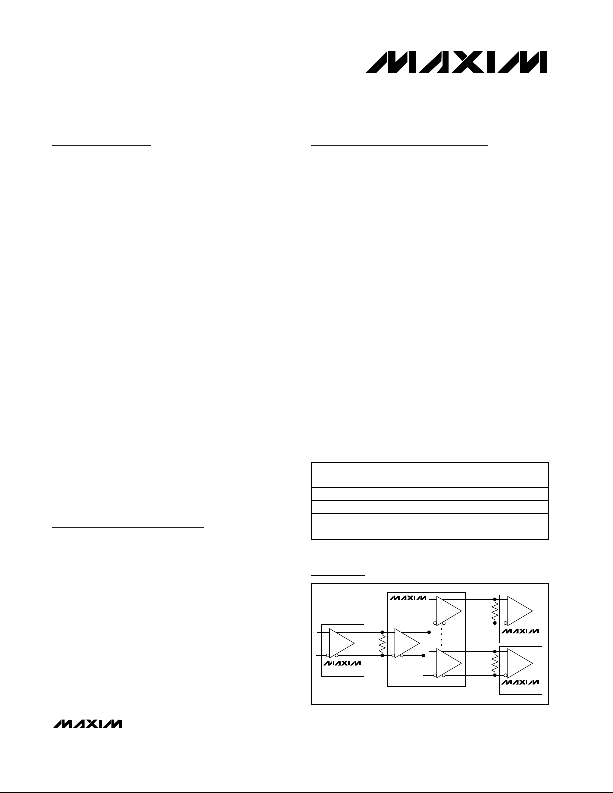
MAX9180
MAX9169
MAX9130
MAX9130
100Ω
LVDS
LVDS
BACKPLANE
OR CABLE
1
4
Rx
Rx
100Ω
100Ω
Typical Application Circuit
19-2616; Rev 0; 10/02
For pricing, delivery, and ordering information, please contact Maxim/Dallas Direct! at
1-888-629-4642, or visit Maxim’s website at www.maxim-ic.com.
Pin Configurations appear at end of data sheet.
PART TEMP RANGE
MAX9169ESE -40°C to +85°C 16 SO LVDS
MAX9169EUE -40°C to +85°C 16 TSSOP LVDS
MAX9170ESE -40°C to +85°C 16 SO LVTTL
MAX9170EUE -40°C to +85°C 16 TSSOP LVTTL
PINPACKAGE
INPUT
Page 2
MAX9169/MAX9170
4-Port LVDS and LVTTL-to-LVDS Repeaters
2 _______________________________________________________________________________________
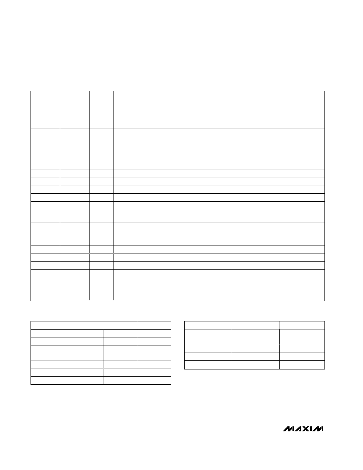
ABSOLUTE MAXIMUM RATINGS
DC ELECTRICAL CHARACTERISTICS
(VCC= 3.0V to 3.6V, RL= 100Ω ±1%, EN_ = high, MAX9169 differential input voltage | V
ID
| = 0.05V to 1.2V, LVDS input common-
mode voltage V
CM
= | VID/2 | to +2.4V - | VID/2 |, TA= -40°C to +85°C, unless otherwise noted. Typical values are at VCC= 3.3V, | VID|
= 0.2V, V
CM
= 1.25V, TA= +25°C for MAX9169. Typical values are at VCC= 3.3V, VIN= 0 or VCC, TA= +25°C for MAX9170.)
(Notes 1 and 2)
Stresses beyond those listed under “Absolute Maximum Ratings” may cause permanent damage to the device. These are stress ratings only, and functional
operation of the device at these or any other conditions beyond those indicated in the operational sections of the specifications is not implied. Exposure to
absolute maximum rating conditions for extended periods may affect device reliability.
VCCto GND..............................................................-0.5V to +4V
Inputs
IN+, IN- to GND....................................................-0.5V to +4V
IN, EN_ to GND ....................................................-0.5V to +6V
Outputs
OUT_+, OUT_- to GND.........................................-0.5V to +4V
Continuous Power Dissipation (T
A
= +70°C)
16-Pin SO (derate 8.7mW/°C above +70°C)................696mW
16-Pin TSSOP (derate 9.4mW/°C above +70°C) .........755mW
Storage Temperature Range .............................-65°C to +150°C
Maximum Junction Temperature .....................................+150°C
ESD Protection
Human Body Model (MAX9169)
(IN+, IN-, OUT_+, OUT_-) ..............................................≥16kV
Human Body Model (MAX9170)
(OUT_+, OUT_-) .............................................................≥10kV
Lead Temperature (soldering, 10s) .................................+300°C
LVDS INPUTS (IN+, IN-) (MAX9169)
PARAMETER SYMBOL CONDITIONS MIN TYP MAX UNITS
Differential Input High Threshold V
Differential Input Low Threshold V
Input Current
(IN+ or IN-, Single Ended)
Power-Off Input Current
(IN+ or IN-, Single Ended)
Input Current I
Power-Off Input Current I
Fail-Safe Input Resistor
Input Capacitance C
+5V TOLERANT LVTTL/LVCMOS INPUTS (IN, EN_)
Input High Voltage V
Input Low Voltage V
Input Current
Input Capacitance (MAX9170) C
LVDS OUTPUTS (OUT_+, OUT_-)
Differential Output Voltage V
Change in VOD Between
Complementary Output States
Steady-State Output Offset
Voltage
TH
TL
V
= 0V, other input open, Figure 1 -2 -11.8 -20
I
IN+, IIN-
I
INO+, IINO-
IN+, IIN-
INO+, IINO-
R
IN1
R
IN2
IN
IH
IL
I
IH
I
IL
IN
OD
∆V
OD
V
OS
IN
V
= +2.4V, other input open, Figure 1 -1.2 -3.2
IN
V
= +1.5V, V
CC
Figure 1
0.05V ≤VID≤ 0.6V, Figure 1 -15 +15
0.6V <VID≤ 1.2V, Figure 1 -20 +20
0.05V ≤VID≤ 0.6V, V
0.6V <VID≤ 1.2V, V
V
= 3.6V, 0 or open, Figure 1 103 138 190
CC
V
= 3.6V, 0 or open, Figure 1 154 210 260
CC
IN+ or IN- to GND (Note 3) 2.2 pF
V
= 2V to 5.5V 20
IN
V
= 0 to 0.8V 10
IN
IN to GND (Note 3) 2.2 pF
Figures 3, 4, 6, 7 250 350 450 mV
Figures 3, 4, 6, 7 1.5 25 mV
Figures 2, 4, 5, 7, 8, 9 1.125 1.26 1.375 V
550mV
-50 -5 mV
= +2.4V, other input open,
IN
= 1.5V, Figure 1 -15 +15
CC
= 1.5V, Figure 1 -20 +20
CC
3.2 20 µA
2.0 5.5 V
0 0.8 V
µA
µA
µA
kΩ
µA
Page 3
MAX9169/MAX9170
4-Port LVDS and LVTTL-to-LVDS Repeaters
_______________________________________________________________________________________ 3
DC ELECTRICAL CHARACTERISTICS (continued)
(VCC= 3.0V to 3.6V, RL= 100Ω ±1%, EN_ = high, MAX9169 differential input voltage | V
ID
| = 0.05V to 1.2V, LVDS input common-
mode voltage V
CM
= | VID/2 | to +2.4V - | VID/2 |, TA= -40°C to +85°C, unless otherwise noted. Typical values are at VCC= 3.3V, | VID|
= 0.2V, V
CM
= 1.25V, TA= +25°C for MAX9169. Typical values are at VCC= 3.3V, VIN= 0 or VCC, TA= +25°C for MAX9170.)
(Notes 1 and 2)
)
PARAMETER SYMBOL CONDITIONS MIN TYP MAX UNITS
Change in VOS Between
Complementary Output States
Peak-to-Peak Output Offset
Voltage
Output Voltage
Fail-Safe Differential Output
Voltage (MAX9169)
High-Impedance Output Current I
Power-Off Output Current I
Output Short-Circuit Current I
Magnitude of Differential Output
Short-Circuit Current
Output Capacitance C
POWER SUPPLY
Supply Current I
Disabled Supply Current I
∆V
V
OS(P-P
V
V
V
OD+
OFF
I
OSD
CC
CCZ
OH
OZ
OS
Figures 2, 4, 5, 7, 8, 9 1.5 25 mV
OS
Figures 8, 9 (Note 4) 40 150 mV
Figures 3, 4, 6, 7 1.65
Figures 3, 4, 6, 7 0.9
OL
IN+, IN- open, undriven and shorted, or
undriven and parallel terminated
EN_ = low, V
V
OUT_- =
OUT_+ =
+3.6V or 0
VCC = +1.5V, V
OUT_- =
+3.6V or 0
V
+3.6V or 0,
OUT_+ =
+3.6V or 0,
VID = +50mV or -50mV,
V
OUT+
= 0 or VCC, V
OUT-
= 0 or V
CC
VID = +50mV or -50mV, VOD = 0 (Note 5) 5.8 10 mA
OUT_+ or OUT_- to GND (Note 6) 3.6 pF
O
DC, RL = 100Ω,
Figures 10, 13
315MHz (630Mbps),
R
= 100Ω, Figures 10, 13
L
EN_ = low
MAX9169 22 30
MAX9170 18 25
MAX9169 43 60
MAX9170 41 55
MAX9169 6.8 8.0
MAX9170 4.3 6.4
+250 +350 +450 mV
-0.5 0.01 +0.5 µA
-0.5 0.01 +0.5 µA
-10 ±5.8 +10 mA
V
mA
mA
Page 4
MAX9169/MAX9170
4-Port LVDS and LVTTL-to-LVDS Repeaters
4 _______________________________________________________________________________________
Note 1: Current into a pin is defined as positive. Current out of a pin is defined as negative. All voltages are referenced to ground
except V
TH
, VTL, VID, VOD, and ∆VOD.
Note 2: Maximum and minimum limits over temperature are guaranteed by design and characterization. Devices are production
tested at T
A
= +25°C.
Note 3: Signal generator output for IN+, IN-, or single-ended IN: V
IN
= 0.4 sin(4E6πt) + 0.5.
Note 4: All input pulses are supplied by a generator having the following characteristics: t
R
or tF≤ 1ns, pulse repetition rate (PRR) =
0.5 Mpps, pulsewidth = 500 ±10ns.
Note 5: Guaranteed by design and characterization.
Note 6: Signal generator output for OUT+ or OUT-: V
IN
= 0.4 sin(4E6πt) + 0.5, EN_ = low.
Note 7: C
L
includes scope probe and test jig capacitance.
Note 8: Signal generator output for differential inputs IN+, IN- (unless otherwise noted): frequency = 50MHz, 49% to 51% duty cycle,
R
O
= 50Ω, tR= 1.0ns, and tF= 1.0ns (0% to 100%). Signal generator output for single-ended input IN (unless otherwise noted):
frequency = 50MHz, 49% to 51% duty cycle, R
O
= 50Ω, VIH= VCC, VIL= 0V, tR= 1.0ns, and tF= 1.0ns (0% to 100%).
Note 9: Signal generator output for MAX9169 t
DJ
: VOH= +1.3V, VOL= +1.1V, data rate = 630Mbps, 223-1 PRBS, RO= 50Ω,
t
R
= 1.0ns and tF= 1.0ns (0% to 100%). Signal generator output for MAX9170 tDJ: VOH= VCC, VOL= 0V, data rate =
630Mbps, 223-1 PRBS, RO= 50Ω, tR= 1.0ns, and tF= 1.0ns (0% to 100%).
Note 10: Signal generator output for MAX9169 t
RJ
: VOH= +1.3V, VOL= +1.1V, frequency = 315MHz, 50% duty cycle, RO= 50Ω,
t
R
= 1.0ns, and tF= 1.0ns (0% to 100%). Signal generator output for MAX9170 tRJ: VOH= VCC, VOL= 0V, frequency =
315MHz, 50% duty cycle, R
O
= 50Ω, tR= 1.0ns, and tF= 1.0ns (0% to 100%).
Note 11: Signal generator output for MAX9169 t
SK(P)
: VOH= +1.4V, VOL= +1.0V, RO= 50Ω, tR= 1.0ns, and tF= 1.0ns (0% to 100%).
Signal generator output for MAX9170 t
SK(P)
: VOH= +3.0, VOL= 0V, RO= 50Ω, tR= 1.0ns, and tF= 1.0ns (0% to 100%).
Note 12: t
SK(0)
is the magnitude of the time difference between t
PLH
or t
PHL
of all drivers of a single device with all of their inputs
connected together.
Note 13: t
SK(PP)
is the magnitude of the difference in propagation delay times between any specified terminals of two devices when
both devices operate with the same supply voltages, at the same temperature, and have identical packages and test circuits.
AC ELECTRICAL CHARACTERISTICS
(VCC= 3.0V to 3.6V, RL= 100Ω ±1%, CL= 10pF, EN_ = high, MAX9169 differential input voltage | V
ID
| = 0.15V to 1.2V, LVDS input
common-mode voltage V
CM
= | VID/2 | to +2.4V - | VID/2 |, TA= -40°C to +85°C, unless otherwise noted. Typical values are at | VID| =
0.2V, V
CM
= 1.25V, VCC= 3.3V, TA= +25°C for MAX9169. Typical values are at VIN= 0 or VCC, V
CC = 3.3V
, T
A
= +25°C for
MAX9170.) (Notes 5, 7, and 8)
PARAMETER SYMBOL CONDITIONS MIN TYP MAX UNITS
Rise Time t
Fall Time t
Added Deterministic Jitter
Added Random Jitter
Differential Propagation Delay
High to Low
Differential Propagation Delay
Low to High
Pulse Skew t
Pulse Skew t
Channel-to-Channel Skew
(Note 12)
PLH
PLH
- t
- t
Differential Part-to-Part Skew
(Note 13)
Disable Time
Enable Time
Figures 10–15 0.6 0.8 1.2 ns
R
Figures 10–15 0.6 0.8 1.2 ns
F
t
PHL
PHL
t
DJ
t
RJ
t
PHL
t
PLH
SKEW
t
SK(P)
t
SK(0)
t
SK(PP)
t
PHZ
t
PLZ
t
PZH
t
PZL
(Note 9) 110 200 ps
(Note 10) 6 8 ps
Figures 10, 11, 13, 14
Figures 10, 11, 13, 14
MAX9169 2.2 3.5 4.2
MAX9170 1.5 2.6 3.2
MAX9169 2.2 3.5 4.2
MAX9170 1.5 2.6 3.2
Figures 10, 11, 13, 14 40 250 ps
Figures 10, 12, 13, 15 (Note 11) 40 150 ps
MAX9169, Figures 10, 11, 12 25 120
MAX9170, Figures 13, 14, 15 15 100
MAX9169, Figures 10, 11, 12 0.28 1.2
MAX9170, Figures 13, 14, 15 0.19 1.2
High to high-Z, Figures 16–19 11 15
Low to high-Z, Figures 16–19 11.8 15
High-Z to high, Figures 16–19 2.3 10
High-Z to low, Figures 16–19 5.8 10
ns
ns
ps
ns
ns
ns
Page 5

MAX9169/MAX9170
4-Port LVDS and LVTTL-to-LVDS Repeaters
_______________________________________________________________________________________ 5
Typical Operating Characteristics
(VCC= 3.3V, RL= 100Ω, CL= 10pF, | VID| = 150mV, VCM= 1.25V, fIN= 50MHz, TA= +25°C, unless otherwise noted.)
MAX9169 SUPPLY CURRENT
vs. FREQUENCY
50
40
2 CHANNELS ACTIVE
30
20
SUPPLY CURRENT (mA)
10
0
0 315
4 CHANNELS ACTIVE
3 CHANNELS ACTIVE
1 CHANNEL ACTIVE
ALL CHANNELS DISABLED
FREQUENCY (MHz)
TRANSITION TIME
vs. TEMPERATURE
840
820
800
780
760
TRANSITION TIME (ns)
740
t
r
MAX9169/70 toc01
SUPPLY CURRENT (mA)
2702251801359045
MAX9169/70 toc04
t
f
PROPAGATION DELAY (ns)
MAX9170 SUPPLY CURRENT
vs. FREQUENCY
40
30
20
10
0
0 315
4 CHANNELS ACTIVE
3 CHANNELS ACTIVE
2 CHANNELS ACTIVE
1 CHANNEL ACTIVE
ALL CHANNELS DISABLED
FREQUENCY (MHz)
MAX9169 PROPAGATION DELAY
vs. TEMPERATURE
3.8
3.7
3.6
t
3.5
3.4
3.3
PHL
t
PLH
DIFFERENTIAL OUTPUT AMPLITUDE
vs. FREQUENCY
360
MAX9169/70 toc02
320
280
VCC = 3.3V
240
DIFFERENTIAL OUTPUT AMPLITUDE (mV)
2702251801359045
200
0 315
VCC = 3.0V
FREQUENCY (MHz)
MAX9170 PROPAGATION DELAY
vs. TEMPERATURE
2.9
2.8
MAX9169/70 toc05
2.7
2.6
PROPAGATION DELAY (ns)
2.5
t
PLH
VCC = 3.6V
t
PHL
MAX9169/70 toc03
2702251801359045
MAX9169/70 toc06
720
-40 85
TEMPERATURE (°C)
DIFFERENTIAL OUTPUT VOLTAGE
600
500
400
300
200
DIFFERENTIAL OUTPUT VOLTAGE (mV)
100
50 150
603510-15
vs. LOAD RESISTOR
LOAD RESISTOR (Ω)
3.2
-40 85
TEMPERATURE (°C)
MAX9169/70 toc07
12510075
603510-15
950
900
850
800
TRANSITION TIME (ps)
750
700
2.4
-40 85
TEMPERATURE (°C)
603510-15
TRANSITION TIME
vs. CAPACITIVE LOAD
MAX9169/70 toc08
t
r
t
f
515
CAPACITIVE LOAD (pF)
131197
Page 6
MAX9169/MAX9170
4-Port LVDS and LVTTL-to-LVDS Repeaters
6 _______________________________________________________________________________________
Pin Description
Table 1. MAX9169 Input/Output Functions
Table 2. MAX9170 Input/Output Functions
PIN
MAX9169 MAX9170
1 1 EN1
2 2 EN2
3 3 EN3
44VCCPower-Supply Voltage. Bypass with 0.1µF and 0.001µF capacitors to ground.
5 5 GND Ground
6 — IN+ Noninverting Differential LVDS Input
7 — IN- Inverting Differential LVDS Input
8 8 EN4
9 9 OUT4- Inverting Differential LVDS Output
10 10 OUT4+ Noninverting Differential LVDS Output
11 11 OUT3- Inverting Differential LVDS Output
12 12 OUT3+ Noninverting Differential LVDS Output
13 13 OUT2- Inverting Differential LVDS Output
14 14 OUT2+ Noninverting Differential LVDS Output
15 15 OUT1- Inverting Differential LVDS Output
16 16 OUT1+ Noninverting Differential LVDS Output
— 6 IN Data Input, 5V Tolerant LVTTL/LVCMOS. Integrated pulldown to GND.
— 7 N.C. No Connection
NAME FUNCTION
OUT1+/OUT1- Enable. +5V tolerant LVTTL/LVCMOS input. Set EN1 high to enable
OUT1+/OUT1-. Set EN1 low to disable OUT1+/OUT1- (high-impedance mode). Integrated
pulldown to GND.
OUT2+/OUT2- Enable. +5V tolerant LVTTL/LVCMOS input. Set EN2 high to enable
OUT2+/OUT2-. Set EN2 low to disable OUT2+/OUT2- (high-impedance mode). Integrated
pulldown to GND.
OUT3+/OUT3- Enable. +5V tolerant LVTTL/LVCMOS input. Set EN3 high to enable
OUT3+/OUT3-. Set EN3 low to disable OUT3+/OUT3- (high-impedance mode). Integrated
pulldown to GND.
OUT4+/OUT4- Enable. +5V tolerant LVTTL/LVCMOS input. Set EN4 high to enable
OUT4+/OUT4-. Set EN4 low to disable OUT4+/OUT4- (high-impedance mode). Integrated
pulldown to GND.
VID = V
+50mV High High
-50mV High Low
Undriven short High High
Undriven parallel terminated High High
INPUT OUTPUT
- V
IN+
IN-
X Low or open High-Z
Open High High
EN_ V
OD
V
X Low or open High-Z
High High High
Low High Low
Open High Low
INPUT OUTPUT
IN
EN_ V
OD
Page 7

Detailed Description
LVDS is a signaling method for point-to-point and
multidrop data communication over a controlled-impedance medium as defined by the ANSI TIA/EIA-644 and
IEEE 1596.3 standards. LVDS uses a lower voltage swing
than other common standards, achieving higher data
rates with reduced power consumption, while reducing
EMI emissions and system susceptibility to noise.
The MAX9169/MAX9170 are 630Mbps, four-port
repeaters for high-speed, low-power applications. The
MAX9169 accepts an LVDS input and has a fail-safe
input circuit. The MAX9170 features a +5V tolerant single-ended LVTTL/LVCMOS input. Both devices repeat
the input at four LVDS outputs. The MAX9169 detects
differential signals as low as 50mV and as high as 1.2V
over a |VID|/2 to 2.4V - |VID|/2 common-mode range.
The MAX9170’s +5V tolerant LVTTL/LVCMOS input
includes circuitry to hold the decision threshold constant at +1.5V over temperature and supply voltage.
The MAX9169/MAX9170 outputs use a current-steering
configuration to generate a 2.5mA to 4.5mA output current. This current-steering approach induces less ground
bounce and shoot-through current, enhancing noise
margin and system speed performance. The outputs are
short-circuit current limited and are high impedance
when disabled or when the device is not powered.
The MAX9169/MAX9170 current-steering output requires
a resistive load to terminate the signal and complete the
transmission loop. Because the devices switch the direction of current flow and not voltage levels, the output voltage swing is determined by the value of the termination
resistor multiplied by the output current. With a typical
3.5mA output current, the MAX9169/MAX9170 produce
a 350mV output voltage when driving a transmission line
terminated with a 100Ω resistor (3.5mA ✕ 100Ω =
350mV). Logic states are determined by the direction of
current flow through the termination resistor.
Fail-Safe Circuitry
The fail-safe feature of the MAX9169 sets the outputs
high when the differential input is:
• Open
• Undriven and shorted
• Undriven and terminated
Without a fail-safe circuit, when the input is undriven,
noise at the input may switch the outputs and it may
appear to the system that data is being sent. Open or
undriven terminated input conditions can occur when a
cable is disconnected or cut, or when an LVDS driver
output is in high impedance. A shorted input can occur
because of cable failure.
When the input is driven with signals meeting the LVDS
standard, the input common-mode voltage is less than
V
CC
- 0.3V and the fail-safe circuit is not activated
(Figure 1). If the input is open, undriven and shorted, or
undriven and parallel terminated, an internal resistor in
the fail-safe circuit pulls both the inputs above VCC-
0.3V, activating the fail-safe circuit and forcing the outputs high.
Applications Information
Supply Bypassing
Bypass VCCwith high-frequency surface-mount ceramic 0.1µF and 0.001µF capacitors in parallel as close to
the device as possible, with the smaller value capacitor
closest to the VCCpin. Use multiple parallel vias to minimize parasitic inductance.
Traces, Cables, and Connectors
The characteristics of differential input and output connections affect the performance of the MAX9169/
MAX9170. Use controlled-impedance traces, cables,
and connectors with matched characteristic impedance.
Ensure that noise couples as common mode by running the traces of a differential pair close together.
Reduce within-pair skew by matching the electrical
length of the traces of a differential pair. Excessive
skew can result in a degradation of magnetic field cancellation. Maintain a constant distance between traces
of a differential pair to avoid discontinuities in differen-
MAX9169/MAX9170
4-Port LVDS and LVTTL-to-LVDS Repeaters
_______________________________________________________________________________________ 7
Figure 1. MAX9169 Input Fail-Safe Circuit
V
CC
R
IN2
COMPARATOR
- 0.3V
V
CC
IN+
R
/2
IN1
R
/2
IN1
IN-
RECEIVER
MAX9169
OUT1+
OUT1-
OUT4+
OUT4-
Page 8

MAX9169/MAX9170
4-Port LVDS and LVTTL-to-LVDS Repeaters
8 _______________________________________________________________________________________
Figure 2. MAX9169 Output Offset Voltage Test Circuit
Test Circuits and Timing Diagrams
tial impedance. Minimize the number of vias to further
prevent impedance discontinuities.
Avoid the use of unbalanced cables, such as ribbon
cable. Balanced cables, such as twisted pair, offer
superior signal quality and tend to generate less EMI
due to canceling effects. Balanced cables tend to pick
up noise as common mode, which is rejected by the
LVDS receiver.
Termination
The MAX9169/MAX9170 LVDS outputs are specified for
a 100Ω load but can drive 90Ω to 132Ω to accommo-
date various types of interconnect. The termination
resistor at the driven receiver should match the differential characteristic impedance of the interconnect and
be located close to the receiver input. Use a ±1% surface-mount termination resistor.
Board Layout
A four-layer PC board with separate layers for power,
ground, and LVDS signals is recommended. Keep
LVTTL/LVCMOS signals separated from the LVDS signals to prevent crosstalk to the LVDS lines.
MAX9169
50Ω
OUT1+
50Ω
50Ω
OUT1-
V
OS
10pF
10pF
50Ω
IN+
IN-
10pF
10pF
PULSE
GENERATOR
50Ω
50Ω
OUT4+
OUT4-
V
OS
Page 9

MAX9169/MAX9170
4-Port LVDS and LVTTL-to-LVDS Repeaters
_______________________________________________________________________________________ 9
Figure 3. MAX9169 Differential Output Voltage Test Circuit
Test Circuits and Timing Diagrams (continued)
Figure 4. MAX9169 Output DC Parameters
MAX9169
50Ω
50Ω
IN+
IN-
PULSE
GENERATOR
IN-
100Ω
100Ω
3.75kΩ
3.75kΩ
3.75kΩ
3.75kΩ
0V ≤ V
0V ≤ V
TEST
TEST
≤ 2.4V
≤ 2.4V
OUT1+
V
OD
OUT1-
OUT4+
V
OD
OUT4-
V
= ((V
) - (V
CM
)) / 2
IN+
IN-
IN+
OUT_-
OUT_+
(OUT_+) - (OUT_-)
V
OS(-)
V
OD_-
0V
DIFFERENTIAL
V
ID
∆VOS = | (V
= | (V
∆V
OD
V
OS(+)
OS(+)
OD_+
V
) - (V
OD_+
) - (V
OS(-)
OD_-
V
OS(-)
OH
V
OL
V
= 0V
OD
V
) |
) |
Page 10

MAX9169/MAX9170
4-Port LVDS and LVTTL-to-LVDS Repeaters
10 ______________________________________________________________________________________
Figure 5. MAX9170 Output Offset Voltage Test Circuit
Test Circuits and Timing Diagrams (continued)
Figure 6. MAX9170 Differential Output Voltage Test Circuit
OUT1+
MAX9170
10pF
10pF
50Ω
50Ω
OUT1-
V
OS
50Ω
IN
PULSE
GENERATOR
MAX9170
PULSE
GENERATOR
IN
OUT1+
OUT1-
OUT4+
OUT4+
50Ω
50Ω
3.75kΩ
3.75kΩ
3.75kΩ
OUT4-
V
OS
0V ≤ V
TEST
≤ 2.4V
10pF
10pF
V
100Ω
OD
50Ω
OUT4-
V
100Ω
OD
0V ≤ V
TEST
3.75kΩ
≤ 2.4V
Page 11

MAX9169/MAX9170
4-Port LVDS and LVTTL-to-LVDS Repeaters
______________________________________________________________________________________ 11
Figure 7. MAX9170 LVDS Output DC Parameters
Test Circuits and Timing Diagrams (continued)
Figure 8. MAX9169 Output Offset Voltage Waveforms
Figure 9. MAX9170 Output Offset Voltage Waveforms
IN
OUT_-
OUT_+
(OUT_+) - (OUT_-)
V
OS(-)
V
OD_-
IN-
IN+
V
OS(-)
V
IH
V
IL
V
OH
1.25V
1.20V
V
OS(-)
V
OL
V
= 0V
OD
V
OS(+)
= | (V
∆V
OS
∆V
= | (V
OD
VID = 50mV
V
OS(P-P)
V
OS(+)
OS(+)
OD_+
) - (V
V
) - (V
OD_+
OS(-)
OD_-
) |
) |
∆V
OS
V
OS(-)
IN
V
OS(-)
V
OS(+)
V
OS(P-P)
3V
0V
∆V
OS
V
OS(-)
Page 12

MAX9169/MAX9170
4-Port LVDS and LVTTL-to-LVDS Repeaters
12 ______________________________________________________________________________________
Figure 10. MAX9169 Propagation Delay and Transition Time Test Circuit
Test Circuits and Timing Diagrams (continued)
Figure 11. MAX9169 Propagation Delay and Transition Time Waveforms
C
L
10pF
10pF
OUT1+
R
L
100Ω
C
L
OUT1-
50Ω
MAX9169
50Ω
IN+
IN-
PULSE
GENERATOR
IN-
V
CM
IN+
V
OD
20%
0V
t
PLH
0V
DIFFERENTIAL
t
R
80%
V
ID
80%
10pF
10pF
t
PHL
C
L
OUT4+
R
L
100Ω
OUT4-
20%
VCM =
V
OD
= (V
(V
IN+
OUT_+
) - (V
2
) - (V
)
IN-
)
OUT_-
C
L
0V
t
F
Page 13

MAX9169/MAX9170
4-Port LVDS and LVTTL-to-LVDS Repeaters
______________________________________________________________________________________ 13
Figure 12. MAX9169 Propagation Delay and Transition Time Waveforms, t
SK(p)
Test Circuits and Timing Diagrams (continued)
Figure 13. MAX9170 Propagation Delay and Transition Time Test Circuit
IN-
= 1.2V VCM = 1.2V
V
CM
IN+
t
PLH
80%
VOD = (V
0V
V
OD
20%
t
R
MAX9170
OUT_+
) - (V
OUT_-
10pF
10pF
1.4V
1.0V
t
PHL
80%
)
C
L
R
L
100Ω
C
L
t
F
OUT1+
OUT1-
0V
20%
50Ω
IN
PULSE
GENERATOR
10pF
10pF
C
L
OUT4+
R
L
100Ω
OUT4-
C
L
Page 14

MAX9169/MAX9170
4-Port LVDS and LVTTL-to-LVDS Repeaters
14 ______________________________________________________________________________________
Figure 14. MAX9170 Propagation Delay and Transition Time Waveforms
Test Circuits and Timing Diagrams (continued)
Figure 15. MAX9170 Propagation Delay and Transition Time Waveforms, t
SK(p)
V
CC
IN
/2 VCC/2
V
CC
t
PLH
80%
0V
VOD = (V
OUT_+
) - (V
OUT_-
)
80%
0V
t
PHL
0V
V
OD
20%
t
R
IN
V
OD
1.5V 1.5V
t
PLH
80%
VOD = (V
20%
0V
t
R
OUT_+
) - (V
OUT_-
20%
t
F
3.0V
0V
t
PHL
80%
)
0V
20%
t
F
Page 15

MAX9169/MAX9170
4-Port LVDS and LVTTL-to-LVDS Repeaters
______________________________________________________________________________________ 15
Figure 16. MAX9169 Enable and Disable Time Test Circuit
Test Circuits and Timing Diagrams (continued)
Figure 17. MAX9170 Enable and Disable Time Test Circuit
MAX9169
1.25V
EN_
IN+
IN-
50Ω
MAX9170
IN
1.20V
1.25V
1.20V
PULSE
GENERATOR
2.0V
10pF
10pF
10pF
C
L
C
L
C
L
50Ω
50Ω
50Ω
OUT_+
1.2V
OUT_-
OUT_+
0.8V
PULSE
GENERATOR
EN_
50Ω
10pF
C
L
50Ω
OUT_-
1.2V
Page 16

MAX9169/MAX9170
4-Port LVDS and LVTTL-to-LVDS Repeaters
16 ______________________________________________________________________________________
Figure 18. MAX9169 Enable and Disable Time Waveforms
Test Circuits and Timing Diagrams (continued)
Figure 19. MAX9170 Enable and Disable Time Waveforms
EN_
1.5V
t
PHZ
1.5V
t
PZH
3V
OV
~1.4V
V
WHEN VID = +50mV
OUT_+
WHEN VID = -50mV
V
OUT_-
V
WHEN VID = -50mV
OUT_+
WHEN VID = +50mV
V
OUT_-
t
PLZ
EN_
1.5V
t
PHZ
V
WHEN VIN = 2.0V
OUT_+
WHEN VIN = 0.8V
V
OUT_-
WHEN VIN = 0.8V
V
OUT_+
WHEN VIN = 2.0V
V
OUT_-
t
PLZ
1.25V
1.15V
1.25V
1.15V
1.5V
1.25V
1.2V
1.2V
1.15V
t
PZL
t
PZH
~1.0V
3V
OV
~1.4V
1.25V
1.2V
1.2V
1.15V
t
PZL
~1.0V
Page 17

MAX9169/MAX9170
4-Port LVDS and LVTTL-to-LVDS Repeaters
______________________________________________________________________________________ 17
Pin Configurations
Chip Information
TRANSISTOR COUNT: 1187
PROCESS: CMOS
TOP VIEW
EN1
1
EN2
2
EN3
3
V
4
CC
GND
5
IN+
6
IN-
7
EN4
8
MAX9169
OUT1+
16
OUT1-
15
OUT2+
14
OUT2-
13
OUT3+
12
OUT3-
11
OUT4+
10
OUT4-
9
TSSOP/SO
EN1
EN2
EN3
V
GND
N.C.
EN4
MAX9170
1
2
3
4
CC
5
IN
6
7
8
OUT1+
16
OUT1-
15
OUT2+
14
OUT2-
13
OUT3+
12
OUT3-
11
OUT4+
10
OUT4-
9
TSSOP/SO
Page 18

Package Information
(The package drawing(s) in this data sheet may not reflect the most current specifications. For the latest package outline information,
go to www.maxim-ic.com/packages.)
MAX9169/MAX9170
4-Port LVDS and LVTTL-to-LVDS Repeaters
18 ______________________________________________________________________________________
TSSOP4.40mm.EPS
Page 19

MAX9169/MAX9170
4-Port LVDS and LVTTL-to-LVDS Repeaters
Maxim cannot assume responsibility for use of any circuitry other than circuitry entirely embodied in a Maxim product. No circuit patent licenses are
implied. Maxim reserves the right to change the circuitry and specifications without notice at any time.
Maxim Integrated Products, 120 San Gabriel Drive, Sunnyvale, CA 94086 408-737-7600 ____________________ 19
© 2002 Maxim Integrated Products Printed USA is a registered trademark of Maxim Integrated Products.
Package Information (continued)
(The package drawing(s) in this data sheet may not reflect the most current specifications. For the latest package outline information,
go to www.maxim-ic.com/packages.)
16L SOIC.EPS
 Loading...