

Page 1
General Description
The MAX9164 high-speed LVDS driver/receiver is
designed specifically for low-power point-to-point applications. The MAX9164 operates from a single 3.3V
power supply, and is pin compatible with DS90LV019.
The device features an independent differential driver
and receiver.
The MAX9164 driver output uses a current-steering
configuration to generate a 3.1mA drive current. The
driver accepts a single-ended input and translates it to
LVDS signals at speeds up to 200Mbps over controlled-impedance media of approximately 100Ω. The
transmission media may be printed circuit board traces
or cables. The enable logic input, DE, is used to enable
or disable the driver.
The MAX9164 receiver detects a differential input as
low as 100mV and translates it to single-ended output
at speeds up to 200Mbps. The enable logic input, RE,
is used to enable or disable the receiver.
Inputs and outputs conform to the ANSI TIA/EIA-644
LVDS standard. The MAX9164 is offered in 14-lead SO
and TSSOP packages, and is specified for operation
from -40°C to +85°C.
Applications
Cell-Phone Base Stations Network Switches/Routers
Add/Drop Muxes Backplane Interconnect
Digital Cross-Connects Clock Distribution
DSLAMs
Features
♦ 3.3V Operation
♦ 35% Lower Power than DS90LV019
♦ 200Mbps Data Signaling Rate
♦ ±1V Common-Mode Range
♦ ±100mV Receiver Sensitivity
♦ Flow-Through Pinout
♦ Receiver Output High for Open Input
MAX9164
3.3V Single LVDS Driver/Receiver
________________________________________________________________ Maxim Integrated Products 1
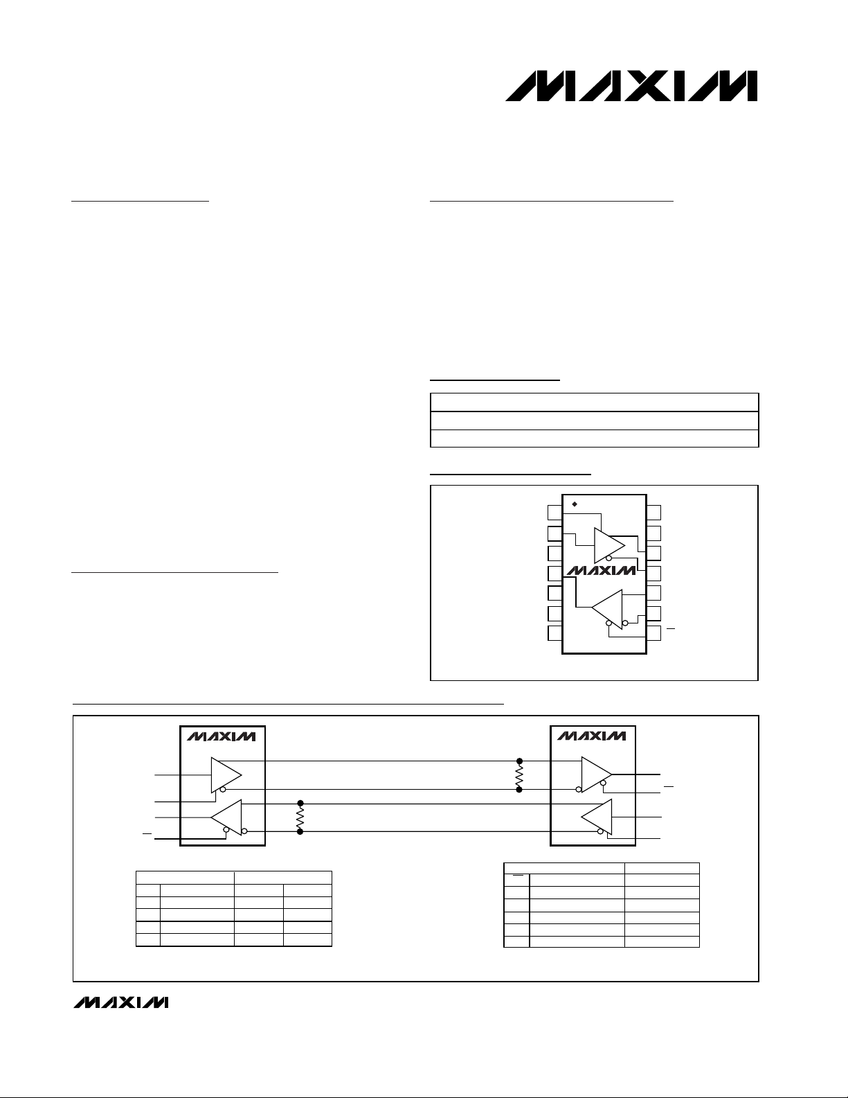
Pin Configuration
Ordering Information
MAX9164
DIN
ROUT
RE
DIN
DE
DO+
DO-
100Ω
RI+
RI-
X: High or low
Z: High impedance
INPUTS
DE
H
H
H
L
DIN
L (≤ 0.8V)
H (≥ 2.0V)
(> 0.8V and < 2.0V)
X
DO+
L
H
Undefined
Z
DO-
H
L
Undefined
Z
TABLE 1. DRIVER FUNCTION TABLE
OUTPUTS
RI+
100Ω
RI-
DO+
DO-
DE
ROUT
RE
MAX9164
X: High or low
Z: High impedance
INPUTS
RE
L
L
L
L
H
RI+ - RI-
L (≤ -100mV)
H(≥ 100mV)
(> -100mV and < 100mV)
Open
X
ROUT
L
H
Undefined
H
Z
TABLE 2. RECEIVER FUNCTION TABLE
OUTPUT
Typical Application Circuit
19-2738; Rev 0; 1/03
For pricing, delivery, and ordering information, please contact Maxim/Dallas Direct! at
1-888-629-4642, or visit Maxim’s website at www.maxim-ic.com.
PART TEMP RANGE PIN-PACKAGE
MAX9164ESD -40°C to +85°C 14 SO
MAX9164EUD -40°C to +85°C 14 TSSOP
TOP VIEW
DIN
N.C.
N.C.
N.C.
DE
1
2
3
4
MAX9164
5
6
7
SO/TSSOP
14
V
CC
N.C.
13
DO+
12
DO-ROUT
11
RI+
10
9
RI-
REGND
8
Page 2
MAX9164
3.3V Single LVDS Driver/Receiver
2 _______________________________________________________________________________________
ABSOLUTE MAXIMUM RATINGS
DC ELECTRICAL CHARACTERISTICS
(VCC= 3.0V to 3.6V, |VID| = 0.1V to 2.4V, common-mode input voltage (VCM) = |VID/2| to 2.4V - |VID|/2, RL= 100Ω ±1%, TA= -40°C to
+85°C. Typical values are at V
CC
= 3.3V, |VID| = 0.2V, VCM= 1.2V, TA= +25°C, unless otherwise noted.) (Notes 1, 2)
Stresses beyond those listed under “Absolute Maximum Ratings” may cause permanent damage to the device. These are stress ratings only, and functional
operation of the device at these or any other conditions beyond those indicated in the operational sections of the specifications is not implied. Exposure to
absolute maximum rating conditions for extended periods may affect device reliability.
VCCto GND...........................................................-0.3V to +4.0V
DO+, DO-, RI+, RI- to GND...................................-0.3V to +4.0V
DIN, ROUT, DE, RE to GND .......................-0.3V to (V
CC
+ 0.3V)
Driver Short-Circuit Current .......................................Continuous
Continuous Power Dissipation (T
A
= +70°C)
14-Pin SO (derate 8.3mW/°C above +70°C)................667mW
14-Pin TSSOP (derate 9.1mW/°C above +70°C) .........727mW
Operating Temperature Range ...........................-40°C to +85°C
Junction Temperature......................................................+150°C
Storage Temperature Range .............................-65°C to +150°C
ESD Protection
HBM (1.5kΩ, 100pF), DO+, DO-, RI+, RI-, DE, RE, DIN,
ROUT ......................................................................> ±2kV
Lead Temperature (soldering, 10s) .................................+300°C
PARAMETER SYMBOL CONDITIONS MIN TYP MAX UNITS
SINGLE-ENDED INPUTS (DIN, DE, RE)
Input High Voltage V
Input Low Voltage V
Input Current I
Input Diode Clamp Voltage V
DRIVER OUTPUT (DO+, DO-)
Differential Output Voltage V
Change in Magnitude of VOD Between
Complementary Output States
Offset Voltage V
Change in Magnitude of V
Complementary Output States
H i g h- Im p ed ance Leakag e C ur r ent I
Power-Off Leakage Current I
Output Short-Circuit Current I
Output Capacitance C
RECEIVER INPUT (RI+, RI-)
Differential Input High Threshold V
Differential Input Low Threshold V
Input Current I
Input Capacitance C
RECEIVER OUTPUT (ROUT)
Output High Voltage V
Output Low Voltage V
Output Short-Circuit Current
IH
IL
RE, DE, DIN = high or low -10 +10 µA
I
CLAMP
Figure 1 250 310 450 mV
Figure 1 0.02 25 mV
OD
Figure 1 1.0 1.29 1.7 V
Figure 1 0.8 25 mV
OS
DE = 0; DO+, DO- = VCC or 0 -1 +1 µA
DO+, DO- = 3.6V or 0; VCC = 0 -1 +1 µA
DO+ = 0 at DIN = V
DO- = 0 at DIN = 0 -3 -10
Capacitance from DO+ or
DO- to 0
TL
VCC = 3.6V or 0;
RI+, RI- = 2.4V or 0
RI+ or RI- to 0 5 pF
RI
IOH = -400µA
IOL = +2.0mA, VID = -100mV 0.025 0.4 V
VID = +100mV, ROUT = 0 -20 -28 -75 mA
Between
OS
∆V
∆V
IN
CL
OD
OS
OZD
OXD
OSD
DO
TH
IN
OH
OL
I
OS
2.0 V
CC
0 0.8 V
= -18mA -1.5 V
CC
-3 -10
3.7 pF
100 mV
-100 mV
-10 +10 µA
VID = 100mV
RI+, RI- open
2.9 3.28 V
V
mA
Page 3
MAX9164
3.3V Single LVDS Driver/Receiver
_______________________________________________________________________________________ 3
DC ELECTRICAL CHARACTERISTICS (continued)
(VCC= 3.0V to 3.6V, |VID| = 0.1V to 2.4V, common-mode input voltage (VCM) = |VID/2| to 2.4V - |VID|/2, RL= 100Ω ±1%, TA= -40°C to
+85°C. Typical values are at V
CC
= 3.3V, |VID| = 0.2V, VCM= 1.2V, TA= +25°C, unless otherwise noted.) (Notes 1, 2)
AC ELECTRICAL CHARACTERISTICS
(VCC= 3.0V to 3.6V, |VID| = 0.2V, VCM= 1.2V, RL= 100Ω ±1%, CL= 10pF, TA= -40°C to +85°C. Typical values are at VCC= 3.3V,
|V
ID
| = 0.2V, VCM= 1.2V, TA= +25°C, unless otherwise noted.) (Notes 3, 4, 5)
Note 1: Maximum and minimum limits over temperature are guaranteed by design and characterization. Devices are 100% tested
at T
A
= +25°C.
Note 2: Current into a pin is defined as positive. Current out of a pin is defined as negative. All voltages are referenced to device
ground except V
TH
, VTL, VID, VOD, and ∆VOD.
Note 3: C
L
includes probe and jig capacitance.
Note 4: AC parameters are guaranteed by design and characterization.
Note 5: Generator waveforms for all tests unless otherwise specified: f = 100MHz, Z
0
= 50Ω, tR = tF = 6.0ns (0 to 3V, 0% to 100%)
for DE and RE, t
R
= tF = 3.0ns (0 to 3V, 0% to 100%) for DIN, and tR = tF = 1.0ns (|VID| = 0.2V, 20% to 80%) for RI+/RI-
inputs.
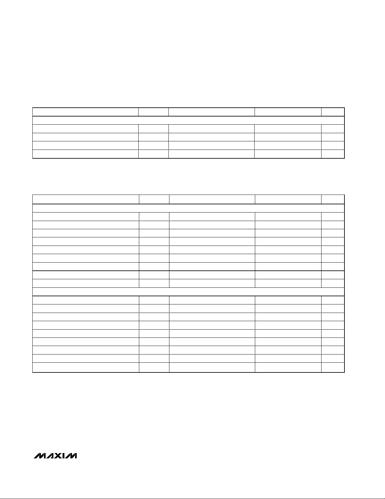
PARAMETER SYMBOL CONDITIONS MIN TYP MAX UNITS
SUPPLY CURRENT
Supply Current I
Driver Supply Current I
Receiver Supply Current I
Disable Supply Current I
CC
CCD
CCR
CCZ
DE = VCC, RE = 0 7.4 12.5 mA
DE = RE = V
CC
7.4 12.5 mA
DE = RE = 0 4.4 7.0 mA
DE = 0, RE = V
CC
4.4 7.0 mA
DRIVER
Differential High-to-Low Propagation Delay t
Differential Low-to-High Propagation Delay t
Differential Skew | t
Rise Time t
Fall Time t
Disable Time High to Z t
Disable Time Low to Z t
Enable Time Z to High t
Enable Time Z to Low t
RECEIVER
Differential High-to-Low Propagation Delay t
Differential Low-to-High Propagation Delay t
Differential Skew | t
Rise Time t
Fall Time t
Disable Time High to Z t
Disable Time Low to Z t
Enable Time Z to High t
Enable Time Z to Low t
PARAMETER SYMBOL CONDITIONS MIN TYP MAX UNITS
Figure 2 2.0 4.4 6.5 ns
Figure 2 1.0 4.2 7.0 ns
Figure 2 0.2 1.0 ns
Figure 2 0.2 0.9 3.0 ns
Figure 2 0.2 0.8 3.0 ns
Figure 3 1.5 6.0 8.0 ns
Figure 3 2.5 5.5 9.0 ns
Figure 3 4.0 5.5 8.0 ns
Figure 3 3.8 5.0 8.0 ns
Figure 4 3.0 5.4 7.0 ns
Figure 4 3.0 5.3 9.0 ns
Figure 4 0.14 1.5 ns
Figure 4 0.15 0.8 3.0 ns
Figure 4 0.15 0.4 3.0 ns
Figure 5 3.0 5.4 6.0 ns
Figure 5 3.0 5.1 6.0 ns
Figure 5 3.0 5.4 8.0 ns
Figure 5 3.0 5.1 8.0 ns
PHLD
PHL
PHLD
PLHD
- t
|t
PLHD
- t
|T
PLH
SKD
TLHD
THLD
PHZ
PLZ
PZH
PZL
PHL
PLH
SK
TLH
THL
PHZ
PLZ
PZH
PZL
Page 4

MAX9164
3.3V Single LVDS Driver/Receiver
4 _______________________________________________________________________________________
Typical Operating Characteristics
(VCC= 3.3V, |VID| = 0.2V, VCM= 1.2V, RL= 100Ω ±1%, FREQ = 100MHz, CL= 10pF, TA= +25°C, unless otherwise noted.)
DRIVER DIFFERENTIAL OUTPUT VOLTAGE
vs. SUPPLY VOLTAGE
MAX9164 toc01
SUPPLY VOLTAGE (V)
DRIVER DIFFERENTIAL OUTPUT VOLTAGE (mV)
3.53.43.33.23.1
307
308
309
310
311
312
313
306
3.0 3.6
DRIVER DIFFERENTIAL OUTPUT VOLTAGE
vs. LOAD RESISTANCE
MAX9164 toc02
LOAD RESISTANCE (Ω)
DRIVER DIFFERENTIAL OUTPUT VOLTAGE (mV)
140130110 12080 90 10070
180
200
220
240
260
280
300
320
340
360
380
400
420
440
460
160
60 150
DRIVER SUPPLY CURRENT
vs. FREQUENCY
MAX9164 toc03
FREQUENCY (MHz)
DRIVER SUPPLY CURRENT (mA)
175150125100755025
8
9
10
11
12
13
7
0 200
SUPPLY CURRENT (ICC)
vs. TEMPERATURE
MAX9164 toc04
TEMPERATURE (°C)
SUPPLY CURRENT (mA)
603510-15
7.2
7.4
7.6
7.8
8.0
7.0
-40 85
DE = HIGH
RE = LOW
DC CURRENT
DRIVER SUPPLY CURRENT (ICC)
vs. SUPPLY VOLTAGE
MAX9164 toc05
SUPPLY VOLTAGE (V)
DRIVER SUPPLY CURRENT (mA)
3.53.43.33.23.1
7.3
7.4
7.5
7.6
7.7
7.8
7.2
3.0 3.6
DE = HIGH
RE = HIGH
DC CURRENT
DRIVER DIFFERENTIAL PROPAGATION
DELAY vs. SUPPLY VOLTAGE
MAX9164 toc06
SUPPLY VOLTAGE (V)
DRIVER DIFFERENTIAL PROPAGATION DELAY (ns)
3.53.43.33.23.1
3.5
4.0
4.5
5.0
5.5
6.0
3.0
3.0 3.6
t
PHLD
t
PLHD
DRIVER DIFFERENTIAL PROPAGATION
DELAY vs. TEMPERATURRE
MAX9164 toc07
TEMPERATURE (°C)
DRIVER PROPAGATION DELAY (ns)
603510-15
3.5
4.0
4.5
5.0
5.5
3.0
-40 85
t
PHLD
t
PLHD
DRIVER DIFFERENTIAL SKEW
vs. SUPPLY VOLTAGE
MAX9164 toc08
SUPPLY VOLTAGE (V)
DRIVER DIFFERENTIAL SKEW (ns)
3.53.43.33.23.1
0.18
0.19
0.20
0.21
0.22
0.23
0.17
3.0 3.6
DRIVER DIFFERENTIAL SKEW
vs. TEMPERATURE
MAX9164 toc09
TEMPERATURE (°C)
DRIVER DIFFERENTIAL SKEW (ns)
603510-15
0.15
0.20
0.25
0.30
0.35
0.10
-40 85
Page 5

MAX9164
3.3V Single LVDS Driver/Receiver
_______________________________________________________________________________________ 5
Typical Operating Characteristics (continued)
(VCC= 3.3V, |VID| = 0.2V, VCM= 1.2V, RL= 100Ω ±1%, FREQ = 100MHz, CL= 10pF, TA= +25°C, unless otherwise noted.)
DRIVER TRANSITION TIME
vs. SUPPLY VOLTAGE
1.3
1.2
1.1
1.0
0.9
0.8
0.7
DRIVER TRANSITION TIME (ns)
0.6
0.5
3.0 3.6
t
THLD
t
TLHD
SUPPLY VOLTAGE (V)
3.53.43.1 3.2 3.3
RECEIVER OUTPUT SHORT-CIRCUIT
CURRENT vs. SUPPLY VOLTAGE
40
35
30
25
20
15
10
5
RECEIVER OUTPUT SHORT-CIRCUIT CURRENT (mA)
0
3.0 3.6
SUPPLY VOLTAGE (V)
VID = +100mV
3.53.43.1 3.2 3.3
RECEIVER DIFFERENTIAL PROPAGATION
DELAY vs. SUPPLY VOLTAGE
7.0
6.5
6.0
5.5
5.0
4.5
4.0
3.5
RECEIVER DIFFERENTIAL PROPAGATION DELAY (ns)
3.0
3.0 3.6
t
PHL
t
PLH
SUPPLY VOLTAGE (V)
3.53.43.1 3.2 3.3
1.6
1.4
MAX9164 toc10
1.2
1.0
0.8
0.6
0.4
DRIVER TRANSITION TIME (ns)
0.2
3.7
3.6
MAX9164 toc13
3.5
3.4
3.3
3.2
3.1
3.0
RECEIVER OUTPUT HIGH VOLTAGE (V)
2.9
2.8
6.00
MAX9164 toc16
5.75
5.50
5.25
5.00
RECEIVER DIFFERENTIAL PROPAGATION DELAY (ns)
4.75
DRIVER TRANSITION TIME
vs. TEMPERATURE
t
TLHD
t
THLD
0
-40 85
TEMPERATURE (°C)
6035-15 10
RECEIVER OUTPUT HIGH VOLTAGE
vs. SUPPLY VOLTAGE
I
= -400µA
LOAD
= +100mV
V
ID
3.0 3.6
SUPPLY VOLTAGE (V)
3.53.43.33.23.1
RECEIVER DIFFERENTIAL PROPAGATION
DELAY vs. TEMPERATURE
t
PHL
t
PLH
-40 85
TEMPERATURE (°C)
603510-15
DRIVER TRANSITION TIME
vs. TOTAL LOAD CAPACITANCE
3.5
3.0
MAX9164 toc11
2.5
2.0
1.5
1.0
DRIVER TRANSITION TIME (ns)
0.5
0
10 35
RECEIVER OUTPUT LOW VOLTAGE
0.029
0.028
MAX9164 toc14
0.027
0.026
0.025
0.024
RECEIVER OUTPUT LOW VOLTAGE (V)
0.023
0.022
3.0 3.6
RECEIVER TRANSITION TIME
vs. TOTAL LOAD CAPACITANCE
3.0
2.5
MAX9164 toc17
2.0
1.5
1.0
RECEIVER TRANSITION TIME (ns)
0.5
0
10 35
t
TLHD
t
THLD
CAPACITANCE (pF)
vs. SUPPLY VOLTAGE
SUPPLY VOLTAGE (V)
t
TLH
t
THL
CAPACITANCE (pF)
30252015
I
LOAD
= -100mV
V
ID
30252015
MAX9164 toc12
MAX9164 toc15
= 2mA
3.53.43.33.23.1
MAX9164 toc18
Page 6

MAX9164
3.3V Single LVDS Driver/Receiver
6 _______________________________________________________________________________________
Pin Description
Figure 1. Differential Driver DC Test Circuit
PIN NAME FUNCTION
1DE
2 DIN LVTTL/LVCMOS Driver Input
3, 5, 6, 13 N.C. No Connection. Not internally connected.
4 ROUT LVTTL/LVCMOS Receiver Output
7 GND Ground
8 RE
9 RI- Inverting LVDS Receiver Input. RI- has an integrated pulldown to GND.
10 RI+ Noninverting LVDS Receiver Input. RI+ has an integrated pullup to VCC.
11 DO- Inverting LVDS Driver Output
12 DO+ Noninverting LVDS Driver Output
14 V
2.0V
0.8V
CC
LVTTL/LVCMOS Driver Enable Input. The driver is enabled when DE is high. When DE is low,
the driver outputs, DO+ and DO-, are disabled and are high impedance.
LVTTL/LVCMOS Receiver Enable Input. The receiver is enabled when RE is low. When RE is
high, the receiver output is disabled and is high impedance.
Power-Supply Input. Bypass VCC to GND with 0.1µF and 0.001µF ceramic capacitors.
DO+
R
/2
L
DIN
RL/2
DO-
V
OS
V
OD
Page 7

MAX9164
3.3V Single LVDS Driver/Receiver
_______________________________________________________________________________________ 7
Figure 2. Driver Differential Propagation Delay and Transition
Time Test Circuit and Waveforms
Figure 3. Driver High-Impedance Delay Test Circuit and
Waveforms
Figure 4. Receiver Propagation Delay and Transition Time Test
Circuit and Waveforms
Figure 5. Receiver High-Impedance Delay Test Circuit and
Waveforms
C
L
PULSE
GENERATOR
50Ω
DIN
R
L
C
L
DO+
DO-
3V
DIN
t
PLHD
1.5V
1.5V
t
PHLD
0V
DO-
DO+
0V
80% 80%
V
OD
V
OD
0V (DIFFERENTIAL)
V
DO+ - DO-
20%
t
TLHD
OD
t
THLD
20%
RI+
RI-
RI+
PULSE
GENERATOR
50Ω
0V DIFF
t
PLH
50Ω
RI-
V
ID
ROUT
C
L
1.3V
V
= 1.2V
CM
t
PHL
1.1V
V
OH
80% 80%
1.5V
V
OL
t
THL
ROUT
1.5V
20% 20%
t
TLH
C
2.0V
0.8V
PULSE
GENERATOR
DO- (DIN = L)
DO+ (DIN = H)
DO- (DIN = H)
DO+ (DIN = L)
L
DIN
C
DE
50Ω
DE
1.5V
t
PHZ
V
OH
t
PLZ
V
OL
L
50%
50%
/2
R
L
/2 1.2V
R
L
1.5V
t
PZH
50%
t
PZL
50%
DO+
DO-
3V
0V
1.2V
1.2V
RI+
PULSE
RI-
RE
C
L
500Ω
V
CC
GENERATOR
50Ω
V
WHEN ROUT IS LOW,
CC
GND WHEN ROUT IS HIGH.
1.5V
1.5V
RE
ROUT
ROUT
t
PHZ
V
- 0.5V
OH
t
PLZ
+ 0.5V
V
OL
t
PZH
50%
t
PZL
50%
ROUT
3V
0V
V
OH
GND
V
CC
V
OL
Page 8

MAX9164
3.3V Single LVDS Driver/Receiver
8 _______________________________________________________________________________________
Detailed Description
The MAX9164 high-speed LVDS driver/receiver is
designed specifically for low-power point-to-point
applications. The MAX9164 operates from a single 3.3V
power supply, and is pin compatible with the
DS90LV019. The device features an independent differential driver and receiver.
The MAX9164 driver outputs use a current-steering
configuration to generate a 3.1mA (typ) output current.
This current-steering approach induces less ground
bounce and no shoot-through current, enhancing noise
margin and system speed performance. The outputs
are short-circuit current limited. The MAX9164 output
requires a resistive load to terminate the signal and
complete the transmission loop. With a typical 3.1mA
output current, the MAX9164 produces a 310mV output
voltage when driving a bus terminated with a 100Ω
resistor (3.1mA x 100Ω = 310mV).
The MAX9164 receiver detects a differential input as
low as 100mV and translates it to single-ended output.
The device features input biasing that drives the output
high if the inputs are left open.
Power-On Reset
The power-on reset voltage of the MAX9164 is typically
2.2V. When the supply falls below this voltage, the
device is disabled and the outputs (DO+, DO-, and
ROUT) are high impedance.
Applications Information
Power-Supply Bypassing
Bypass VCCwith high-frequency, surface-mount
ceramic 0.1µF and 0.001µF capacitors in parallel as
close to the device as possible, with the smaller valued
capacitor closest to VCC.
Termination
The MAX9164 requires an external termination resistor
at the differential input. This termination resistor should
match the differential impedance of the input transmission line.
The differential output requires a termination resistor at
the far end of the transmission line. This termination
resistor should match the differential impedance of the
output transmission line.
These termination resistors are typically 100Ω. Minimize the distance between the input termination resistor and the MAX9164 receiver input.
Traces, Cables, and Connectors
The characteristics of differential input and output connections affect the performance of the device. Use
controlled-impedance traces, cables, and connectors
with matched characteristic impedance.
Ensure that noise couples as common mode by running the traces of a differential pair close together.
Reduce within-pair skew by matching the electrical
length of the conductors within a differential pair.
Excessive skew can result in a degradation of magnetic field cancellation.
Maintain the distance between conductors within a differential pair to avoid discontinuities in differential
impedance. Minimize the number of vias to further prevent impedance discontinuities.
Board Layout
For LVDS applications, a four-layer PC board with separate power, ground, LVDS, and logic signal layers is
recommended. Separate the LVTTL/LVCMOS and
LVDS signals to prevent coupling.
Chip Information
TRANSISTOR COUNT: 901
PROCESS: CMOS
Page 9

MAX9164
3.3V Single LVDS Driver/Receiver
_______________________________________________________________________________________ 9
Package Information
(The package drawing(s) in this data sheet may not reflect the most current specifications. For the latest package outline information
go to www.maxim-ic.com/packages
.)
N
1
TOP VIEW
D
e
FRONT VIEW
INCHES
DIM
MIN
0.053A
0.004
A1
0.014
B
0.007
C
e 0.050 BSC 1.27 BSC
0.150
HE
A
B
A1
C
L
E
H 0.2440.228 5.80 6.20
0.016L
VARIATIONS:
INCHES
MINDIM
D
0.189 0.197 AA5.004.80 8
0.337 0.344 AB8.758.55 14
D
0-8
SIDE VIEW
MAX
0.069
0.010
0.019
0.010
0.157
0.050
MAX
0.3940.386D
MILLIMETERS
MAX
MIN
1.35
1.75
0.10
0.25
0.35
0.49
0.19
0.25
3.80 4.00
0.40 1.27
MILLIMETERS
MAX
MIN
9.80 10.00
N MS012
16
AC
SOICN .EPS
PROPRIETARY INFORMATION
TITLE:
PACKAGE OUTLINE, .150" SOIC
REV.DOCUMENT CONTROL NO.APPROVAL
21-0041
1
B
1
Page 10

MAX9164
3.3V Single LVDS Driver/Receiver
Maxim cannot assume responsibility for use of any circuitry other than circuitry entirely embodied in a Maxim product. No circuit patent licenses are
implied. Maxim reserves the right to change the circuitry and specifications without notice at any time.
10 ____________________Maxim Integrated Products, 120 San Gabriel Drive, Sunnyvale, CA 94086 408-737-7600
© 2003 Maxim Integrated Products Printed USA is a registered trademark of Maxim Integrated Products.
Package Information (continued)
(The package drawing(s) in this data sheet may not reflect the most current specifications. For the latest package outline information
go to www.maxim-ic.com/packages
.)
TSSOP4.40mm.EPS
 Loading...