

Page 1
General Description
The MAX9160 125MHz, 14-port LVTTL/LVCMOS clock
driver repeats the selected LVDS or LVTTL/LVCMOS
input on two output banks. Each bank consists of seven
LVTTL/LVCMOS series terminated outputs and a bank
enable. The LVDS input has a fail-safe function. The
MAX9160 has a propagation delay that can be adjusted
using an external resistor to set the bias current for an
internal delay cell. The LVTTL/LVCMOS outputs feature
200ps maximum output-to-output skew and ±100ps maximum added peak-to-peak jitter.
The MAX9160 is designed to operate with a 3.3V supply voltage over the extended temperature range of
-40°C to +85°C. This device is available in 28-pin
exposed- and nonexposed-pad TSSOP and 32-lead
5mm x 5mm QFN packages.
Applications
Features
♦ LVDS or LVTTL/LVCMOS Input Selection
♦ LVDS Input Fail-Safe Sets Outputs High for Open,
Undriven Short, or Undriven Parallel Termination
♦ Two Output Banks with Separate Bank Enables
♦ Integrated Output Series Termination for 60Ω
Lines
♦ 200ps (max) Output-to-Output Skew
♦ ±100ps (max) Peak-to-Peak Added Output Jitter
♦ 42% to 58% Output Duty Cycle at 125MHz
♦ Guaranteed 125MHz Operating Frequency
♦ LVDS Input Is High Impedance with V
CC
= 0V
or Open (Hot Swappable)
♦ 28-Pin Exposed- and Nonexposed-Pad TSSOP
or 32-Lead QFN Packages
♦ -40°C to +85°C Operating Temperature
♦ 3.0V to 3.6V Supply Voltage
MAX9160
LVDS or LVTTL/LVCMOS Input to
14 LVTTL/LVCMOS Output Clock Driver
________________________________________________________________ Maxim Integrated Products 1
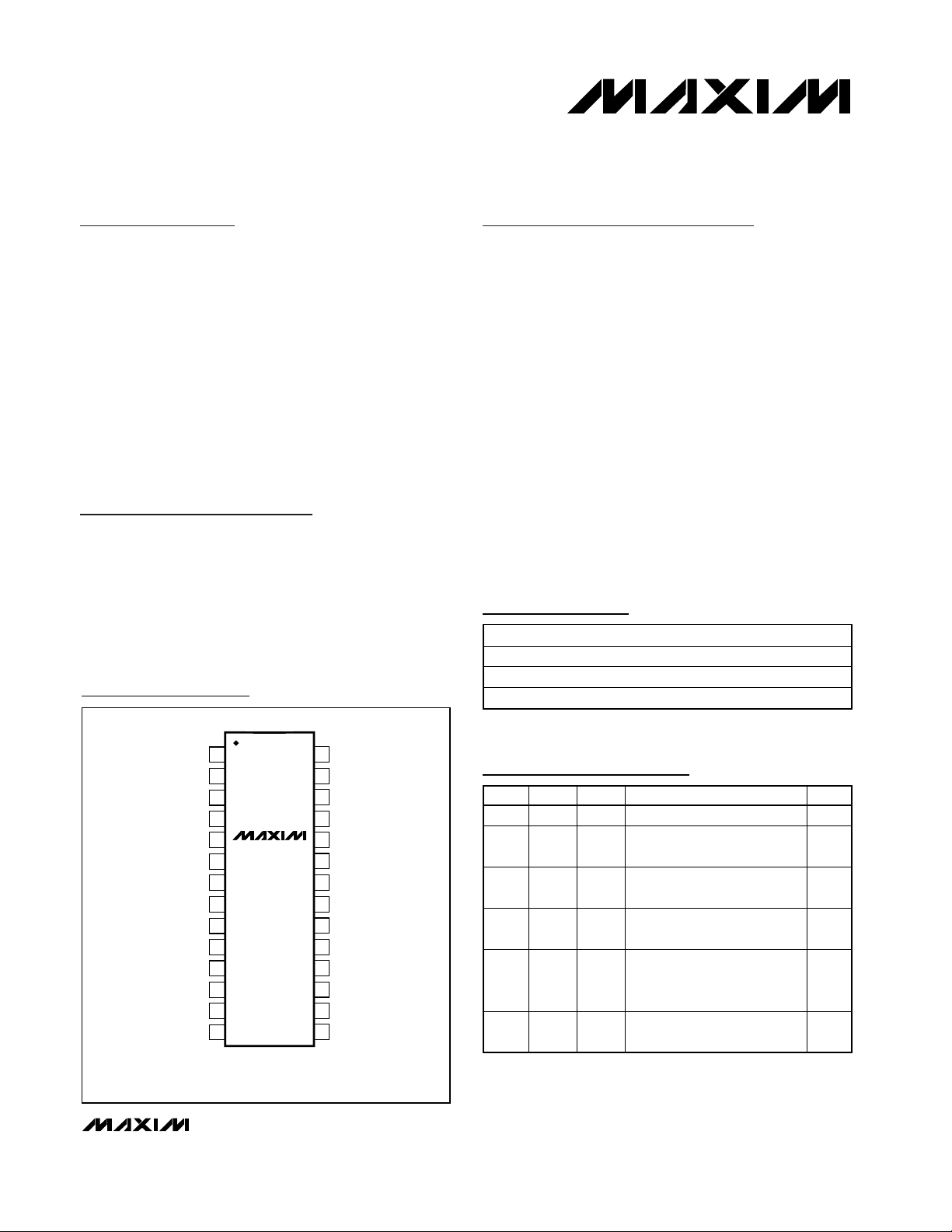
Pin Configurations
Ordering Information
Function Table
19-2392; Rev 0; 4/02
For pricing, delivery, and ordering information, please contact Maxim/Dallas Direct! at
1-888-629-4642, or visit Maxim’s website at www.maxim-ic.com.
Typical Application Circuit and Functional Diagram appear
at end of data sheet.
VID= V
IN+
- V
IN-
H = high logic level
L = low logic level
X = don’t care
Cellular Base Stations
Servers
Add/Drop Multiplexers
Digital Cross-Connects
DSLAMs
Networking Equipment
*Future product—contact factory for availability.
**Exposed pad.
Pin Configurations continued at end of data sheet.
TOP VIEW
1
OUTA5
2
OUTA6
3
ENA
4
SEL
5
SE_IN
V
CC
GND
IN+
IN-
GND
RSET
ENB
OUTB0
OUTB1
MAX9160
6
7
8
9
10
11
12
13
14
TSSOP
28
OUTA4
27
OUTA3
26
GND
25
OUTA2
24
OUTA1
23
V
CC
22
OUTA0
21
OUTB6
20
GND
19
OUTB5
18
OUTB4
17
V
CC
16
OUTB3
15
OUTB2
PART TEMP RANGE PIN-PACKAGE
MAX9160EUI -40°C to +85°C 28 TSSOP
MAX9160AEUI -40°C to +85°C 28 TSSOP-EP**
MAX9160EGJ* -40°C to +85°C 32 QFN-EP
EN_ SEL SE_IN V
HHH X H
HH
L or
H
open
L or
H
open
L or
H
open
L or
Open
XXXL
ID
L or
open
X ≥ +50mV H
X ≤ -50mV L
X
Op en, und r i ven shor t, or
und r i ven p ar al l el ter m i nati on
XL
OUT_
H
Page 2
MAX9160
LVDS or LVTTL/LVCMOS Input to
14 LVTTL/LVCMOS Output Clock Driver
2 _______________________________________________________________________________________
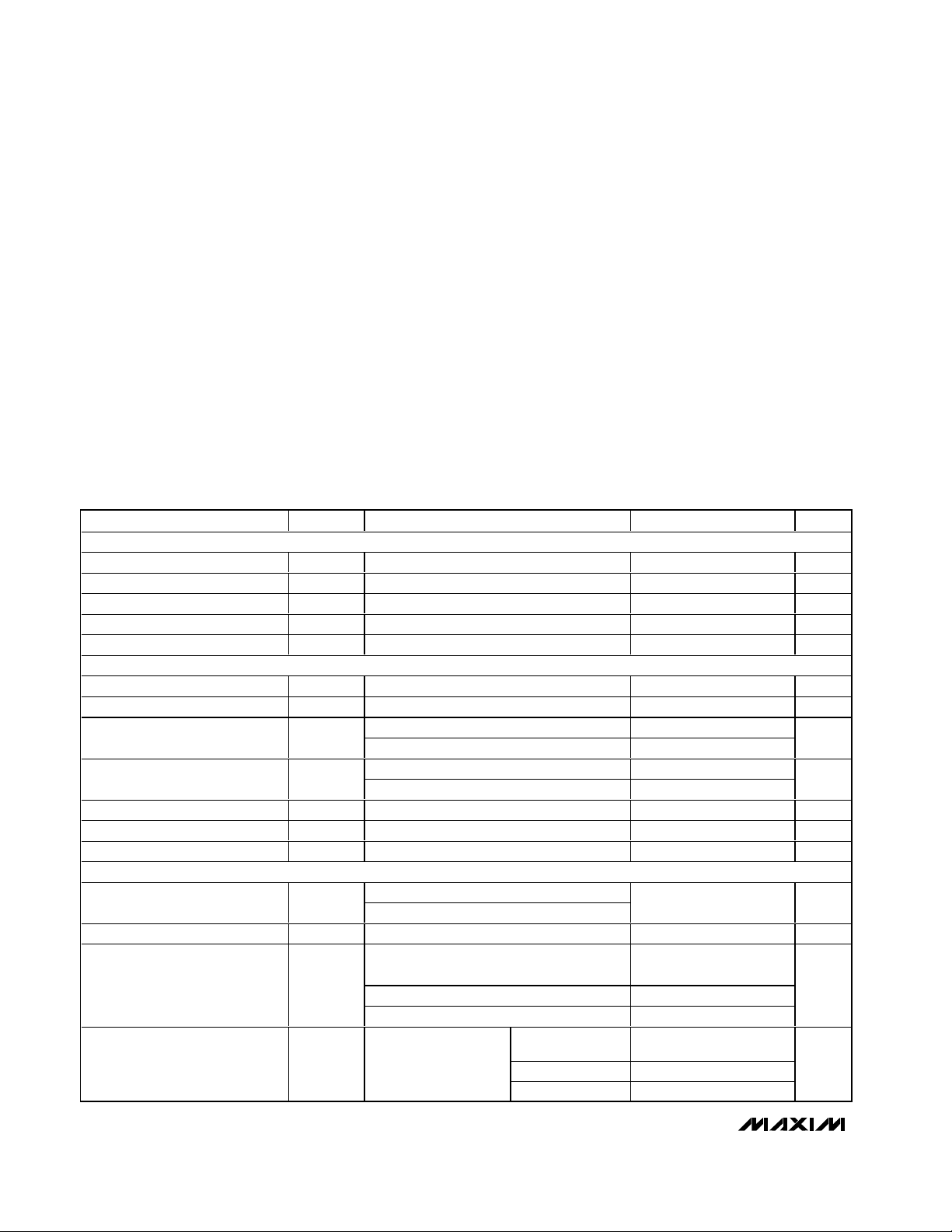
ABSOLUTE MAXIMUM RATINGS
DC ELECTRICAL CHARACTERISTICS
(VCC= 3.0V to 3.6V, ENA = ENB = high, RSET = 12kΩ±1%, differential input voltage IVIDI = 0.05V to 1.2V, input common-mode voltage V
CM
= IVID/2 I to 2.4V - IVID/2 I, TA= -40°C to +85°C, unless otherwise noted. Typical values are at VCC= 3.3V, IVIDI = 0.2V,
V
CM
= 1.2V, TA = +25°C.) (Notes 2, 3)
Stresses beyond those listed under “Absolute Maximum Ratings” may cause permanent damage to the device. These are stress ratings only, and functional
operation of the device at these or any other conditions beyond those indicated in the operational sections of the specifications is not implied. Exposure to
absolute maximum rating conditions for extended periods may affect device reliability.
V
CC
to GND ..............................................................-0.3V to +4V
IN+, IN- to GND........................................................-0.3V to +4V
SE_IN, EN_, SEL, RSET, OUT_ to GND ........-0.3V to V
CC
+ 0.3V
Output Short-Circuit Duration (OUT_) (Note 1) ..........Continuous
Continuous Power Dissipation (T
A
= +70°C)
28-Pin TSSOP (derate 12.8mW/°C above +70°C) .....1024mW
28-Pin TSSOP-EP (derate 23.8mW/°C above +70°C) ..1904mW
32-Pin QFN (derate 21.2mW/°C above +70°C) .........1704mW
Storage Temperature Range .............................-65°C to +150°C
Junction Temperature......................................................+150°C
Operating Temperature Range ...........................-40°C to +85°C
ESD Protection
Human Body Model (IN+, IN-) .......................................±16kV
Human Body Model (SE_IN) ............................................±8kV
Soldering Temperature (10s) ...........................................+300°C
Note 1: Short one output at a time. Do not exceed the absolute maximum junction temperature.
SINGLE-ENDED INPUTS (SE_IN, ENA, ENB, SEL)
Input High Voltage V
Input Low Voltage V
Input Clamp Voltage V
Input Current I
SE_IN Capacitance (Note 4) C
LVDS INPUT (IN+, IN-)
Differential Input High Threshold V
Differential Input Low Threshold V
Input Current I
Power-Off Input Current
Input Resistor 1 R
Input Resistor 2 R
Input Capacitance (Note 4) C
OUTPUTS (OUT_)
Output Short-Circuit Current
(Note 1)
Output Capacitance (Note 4) C
Output High Voltage V
Fail-Safe Output High Voltage V
PARAMETER SYMBOL CONDITIONS MIN TYP MAX UNITS
IH
IL
ICL = -18mA -1.5 -0.85 V
CL
VIN = high or low -20 +20 µA
IN
SE_IN to GND 6.1 pF
IN
TH
TL
0.05V ≤ IVIDI ≤ 0.6V -15 +15
, I
IN+
IN-
0.6V < IVIDI ≤ 1.2V -20 +20
I
IN+(off)
I
IN-(off)
IN1
IN2
I
OS
OH
OHFS
0.05V ≤ IVIDI ≤ 0.6V, VCC = 0V or open -15 +15
0.6V < IVIDI ≤ 1.2V, VCC = 0V or open -20 +20
VCC = 3.6V or 0V, Figure 1 51 100 kΩ
VCC = 3.6V or 0 V, Figure 1 200 341 kΩ
IN+ or IN- to GND 6.0 pF
IN
SEL = high, SE_IN = high, V
SEL = low, VID = 100mV, V
OUT_ to GND 9 pF
O
IOH = -100µA
IOH = -4mA 2.4
IOH = -8mA 2.1
SEL = low, inputs
open, undriven short,
or undriven parallel
terminated
2.0 V
GND 0.8 V
-50 mV
= 0V
OUT
= 0V
OUT
IOH = -100µA
IOH = -4mA 2.4
I
= -8mA 2.1
OH
-115 -30 mA
V
CC
0.2
V
CC
0.2
-
-
CC
50 mV
V
µA
µA
V
V
Page 3
MAX9160
LVDS or LVTTL/LVCMOS Input to
14 LVTTL/LVCMOS Output Clock Driver
_______________________________________________________________________________________ 3
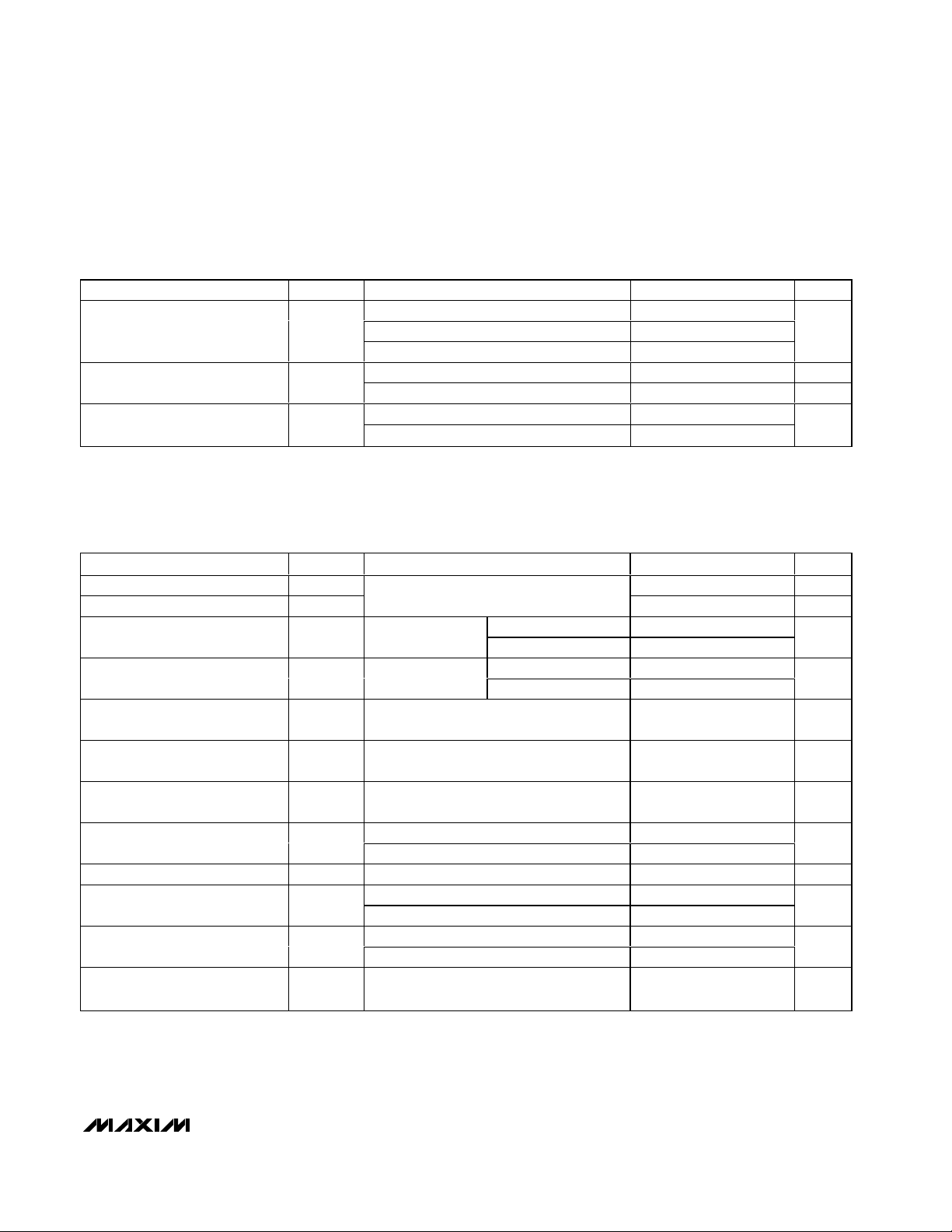
DC ELECTRICAL CHARACTERISTICS (continued)
(VCC= 3.0V to 3.6V, ENA = ENB = high, RSET = 12kΩ±1%, differential input voltage IVIDI = 0.05V to 1.2V, input common-mode voltage V
CM
= IVID/2 I to 2.4V - IVID/2 I, TA= -40°C to +85°C, unless otherwise noted. Typical values are at VCC= 3.3V, IVIDI = 0.2V,
V
CM
= 1.2V, TA = +25°C.) (Notes 2, 3)
AC ELECTRICAL CHARACTERISTICS
(VCC= 3.0V to 3.6V, CL= 20pF, ENA = ENB = high, SEL = high or low, RSET = 12kΩ±1%, differential input voltage IVIDI = 0.15V to
1.2V, input common-mode voltage V
CM
= IVID/2I to 2.4V - IVID/2 I, TA= -40°C to +85°C, unless otherwise noted. Typical values are at
V
CC
= 3.3V, IVIDI = 0.2V, VCM= 1.2V, TA = +25°C.) (Notes 6, 7, 8)
Note 2: Current into a pin is defined as positive. Current out of a pin is defined as negative. All voltages are referenced to ground
except V
TH
, VTL, and VID.
Note 3: Parameter limits over temperature are guaranteed by design and characterization. Devices are production tested at
T
A
= +25°C.
Supply Current I
Output Series Resistance
(Note 5)
PARAMETER SYMBOL CONDITIONS MIN TYP MAX UNITS
IOL = 100µA 0.2
OL
CC
R
IOL = 4mA 0.4Output Low Voltage V
IOL = 8mA 0.8
SEL = high, SE_IN = high or low, no load 15 µA
SEL = low, V
Output switched high, V
S
Output switched low, V
= -100mV or 100mV, no load 7.0 10 mA
ID
= 1.65V 72
OUT
= 1.65V 61
OUT
V
Ω
Rise Time t
Fall Time t
Low-to-High Propagation Delay
IN+, IN- to OUT_
High-to-Low Propagation Delay
IN+, IN- to OUT_
Low-to-High Propagation Delay
SE_IN to OUT_
High-to-Low Propagation Delay
SE_IN to OUT_
Added Peak-to-Peak Output Jitter t
Output Duty Cycle ODC
Outp ut- to- Outp ut S kew ( N ote 9) t
Part-to-Part Skew (Note 10) t
Part-to-Part Skew (Note 11) t
Maximum Switching Frequency
(Note 12)
PARAMETER SYMBOL CONDITIONS MIN TYP MAX UNITS
R
F
t
PLH1
t
PHL1
t
PLH2
t
PHL2
J
SKOO
SKPP1
SKPP2
f
MAX
Figures 2 and 3
SEL = low
SEL = low
SEL = high 2.2 2.9 3.8 ns
SEL = high 2.2 3.1 3.8 ns
100mV peak-to-peak supply noise at
200kHz, 3.3V supply
f
= 125MHz 42 58
IN
f
= 35MHz 48.75 51.25
IN
SE_IN to OUT_, SEL = high 0.9
IN+, IN- to OUT_, SEL = low 2.2
SE_IN to OUT_, SEL = high 1.6
IN+, IN- to OUT_, SEL = low 2.7
RSET = 12kΩ 5.3 6.5 8.0
RSET = open 4.9 9.0
RSET = 12kΩ 5.3 6.4 8.0
RSET = open 4.9 9.0
1.4 2.95 ns
1.4 2.95 ns
100 ps
200 ps
125 MHz
ns
ns
%
ns
ns
Page 4
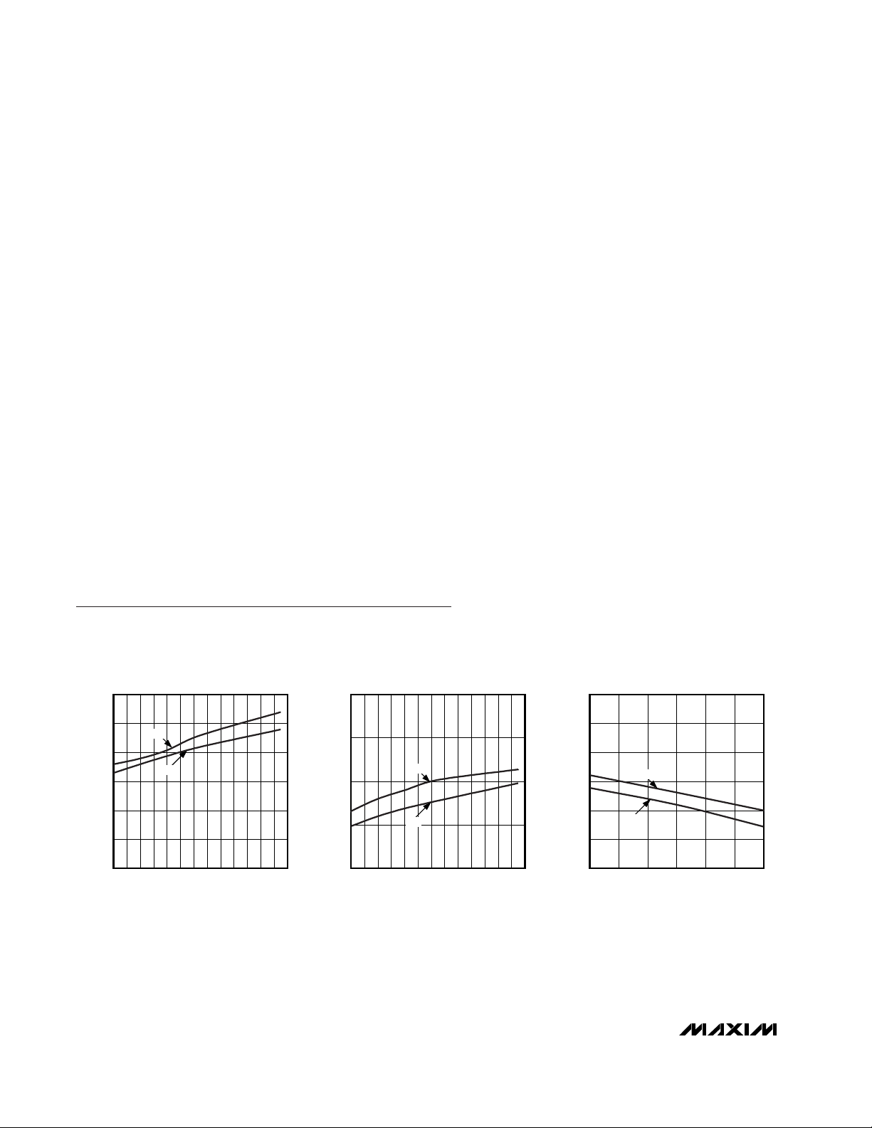
Typical Operating Characteristics
(MAX9160 with RSET = 12kΩ±1%, VCC= 3.3V, CL= 20pF, ENA = ENB = high, IVIDI = 0.2, V
CM
= 1.2V, f
IN
= 125MHz, TA= +25°C,
unless otherwise noted.)
MAX9160
LVDS or LVTTL/LVCMOS Input to
14 LVTTL/LVCMOS Output Clock Driver
4 _______________________________________________________________________________________
AC ELECTRICAL CHARACTERISTICS (continued)
(VCC= 3.0V to 3.6V, CL= 20pF, ENA = ENB = high, SEL = high or low, RSET = 12kΩ±1%, differential input voltage IVIDI = 0.15V to
1.2V, input common-mode voltage V
CM
= IVID/2I to 2.4V - IVID/2 I, TA= -40°C to +85°C, unless otherwise noted. Typical values are at
V
CC
= 3.3V, IVIDI = 0.2V, VCM= 1.2V, TA = +25°C.) (Notes 6, 7, 8)
Note 4: Guaranteed by design and characterization.
Note 5: Total of driver output resistance and integrated series resistor.
Note 6: AC parameters are guaranteed by design and characterization and are not production tested. Limits are set at ±6 sigma.
Note 7: C
L
includes scope probe and test jig capacitance.
Note 8: Pulse generator conditions for SE_IN input: frequency = 125MHz, 50% duty cycle, Z
O
= 50Ω, tR= 1.2ns, and tF= 1.2ns (20%
to 80%), V
OH
= V
CC, VOL
= 0V. Pulse generator conditions for IN+, IN- input: frequency = 125MHz, 50% duty cycle, ZO=
50Ω, t
R
= 1ns, and tF= 1ns (20% to 80%). VID, VCMas specified in AC Electrical Characteristics general
conditions.
Note 9: Measured between outputs with identical loads at V
CC
/2 for a same-edge transition.
Note 10: t
SKPP1
is the greatest difference in propagation delay between different parts operating under identical conditions within
rated conditions.
Note 11: t
SKPP2
is the greatest difference in propagation delay between different parts operating within rated conditions.
Note 12: All AC specifications met at f
MAX
.
DIFFERENTIAL PROPAGATION DELAY
vs. SUPPLY VOLTAGE
MAX9160 toc03
SUPPLY VOLTAGE (V)
DIFFERENTIAL PROPAGATION DELAY (ns)
3.53.43.33.23.1
5.7
6.2
6.7
7.2
7.7
8.2
5.2
3.0 3.6
t
PLH
t
PHL
SINGLE-ENDED PROPAGATION DELAY
vs. TEMPERATURE
MAX9160 toc02
TEMPERATURE (°C)
SINGLE-ENDED PROPAGATION DELAY (ns)
80706050403020100-10-20-30
2.5
3.0
3.5
4.0
2.0
-40 90
t
PHL
t
PLH
DIFFERENTIAL PROPAGATION DELAY
vs. TEMPERATURE
MAX9160 toc01
TEMPERATURE (°C)
DIFFERENTIAL PROPAGATION DEALY (ns)
80706050403020100-10-20-30
4.7
5.2
5.7
6.2
6.7
7.2
4.2
-40 90
t
PLH
t
PHL
Page 5

MAX9160
LVDS or LVTTL/LVCMOS Input to
14 LVTTL/LVCMOS Output Clock Driver
_______________________________________________________________________________________ 5
Typical Operating Characteristics (continued)
(MAX9160 with RSET = 12kΩ±1%, VCC= 3.3V, CL= 20pF, ENA = ENB = high, IVIDI = 0.2, V
CM
= 1.2V, f
IN
= 125MHz, TA= +25°C,
unless otherwise noted.)
SINGLE-ENDED PROPAGATION DELAY
vs. SUPPLY VOLTAGE
4.0
3.5
3.0
2.5
2.0
1.5
1.0
0.5
SINGLE-ENDED PROPAGATION DELAY (ns)
0
t
PHL
t
PLH
3.0 3.6
SUPPLY VOLTAGE (V)
3.53.43.1 3.2 3.3
MAX9160 toc04
OUTPUT VOLTAGE LOW
vs. TEMPERATURE
0.30
0.25
0.20
0.15
0.10
OUTPUT VOLTAGE LOW (V)
0.05
0
-40 90
TEMPERATURE (°C)
I
LOAD
MAX9160 toc07
= 4mA
80706050403020100-10-20-30
SUPPLY CURRENT vs. FREQUENCY
200
ALL CHANNELS SWITCHING
180
CL = 18pF
SINGLE-ENDED INPUT
160
140
120
100
80
60
SUPPLY CURRENT (mA)
40
20
0
0120
FREQUENCY (MHz)
MAX9160 toc10
1059060 7530 4515
DIFFERENTIAL PROPAGATION DELAY
vs. COMMON-MODE VOLTAGE
8.2
7.7
7.2
t
6.7
6.2
5.7
5.2
4.7
DIFFERENTIAL PROPAGATION DELAY (ns)
4.2
0.1 2.1
PLH
t
PHL
1.61.10.6
COMMON-MODE VOLTAGE (V)
OUTPUT VOLTAGE HIGH
vs. SUPPLY VOLTAGE
4.0
3.5
3.0
2.5
2.0
1.5
OUTPUT VOLTAGE HIGH (V)
1.0
0.5
0
3.0 3.6
I
= -4mA
LOAD
SUPPLY VOLTAGE (V)
DIFFERENTIAL PROPAGATION DELAY
vs. OUTPUT CAPACITANCE
14
12
10
8
6
4
2
DIFFERENTIAL PROPAGATION DELAY (ns)
0
15 90
t
PLH
t
PHL
OUTPUT CAPACITANCE (pF)
MAX9160 toc05
MAX9160 toc08
3.53.43.1 3.2 3.3
MAX9160 toc11
75604530
OUTPUT VOLTAGE HIGH
vs. TEMPERATURE
3.20
I
= -4mA
LOAD
3.15
3.10
OUTPUT VOLTAGE HIGH (V)
3.05
3.00
-40 90
TEMPERATURE (°C)
OUTPUT VOLTAGE LOW
vs. SUPPLY VOLTAGE
0.25
0.24
0.23
0.22
OUTPUT VOLTAGE LOW (V)
0.21
I
= 4mA
LOAD
0.20
3.0 3.6
SUPPLY VOLTAGE (V)
TRANSITION TIME
vs. TEMPERATURE
3.0
2.5
2.0
TRANSITION TIME (ns)
1.5
1.0
-40 90
t
R
t
F
TEMPERATURE (°C)
MAX9160 toc06
80706050403020100-10-20-30
MAX9160 toc09
3.53.43.33.23.1
MAX9160 toc12
80706050403020100-10-20-30
Page 6

MAX9160
LVDS or LVTTL/LVCMOS Input to
14 LVTTL/LVCMOS Output Clock Driver
6 _______________________________________________________________________________________
Pin Description
DIFFERENTIAL PROPAGATION DELAY
vs. RSET
MAX9160 toc14
RSET (kΩ)
DIFFERENTIAL PROPAGATION DELAY (ns)
1510
1
2
3
4
5
6
7
8
9
10
0
520
t
PLH
t
PHL
OUTPUT JITTER vs. 200kHz
SUPPLY NOISE AMPLITUDE
MAX9160 toc15
SUPPLY NOISE AMPLITUDE (mV
P-P
)
OUTPUT JITTER (ps
P-P
)
25020015010050
50
100
150
200
250
300
0
0 300
DIFFERENTIAL INPUT
TRANSITION TIME vs. SUPPLY VOLTAGE
MAX9160 toc13
SUPPLY VOLTAGE (V)
TRANSITION TIME (ns)
3.53.43.33.23.1
1.5
2.0
2.5
3.0
1.0
3.0 3.6
t
R
t
F
Typical Operating Characteristics (continued)
(MAX9160 with RSET = 12kΩ±1%, VCC= 3.3V, CL= 20pF, ENA = ENB = high, IVIDI = 0.2, V
CM
= 1.2V, f
IN
= 125MHz, TA= +25°C,
unless otherwise noted.)
PIN
NAME FUNCTION
QFN TSSOP
1 4 SEL
2 5 SE_IN LVCMOS/LVTTL Level Input. SE_IN is pulled to GND by an internal resistor.
3, 12, 16,
22, 29
4, 7, 13,
19, 25, 28
6, 17, 23 V
CC
7, 10, 20, 26 GND Ground
5 8 IN+ Noninverting Input of Differential Input
6 9 IN- Inverting Input of Differential Input
8 11 RSET
9 12 ENB
10, 11, 14, 15,
17, 18, 20
13–16, 18,
19, 21
OUTB_ Bank B LVCMOS/LVTTL Outputs
LVCMOS/LVTTL Level Logic Input. SEL = high selects SE_IN. SEL = low or
open selects IN+, IN-. SEL is pulled to GND by an internal resistor.
Positive Supply Voltage. Bypass with 0.1µF and 0.001µF capacitors to ground.
Connect a 12kΩ ±1% resistor to ground to decrease the minimum to maximum
IN+, IN- to OUT_ propagation delay.
LVCMOS/LVTTL Level Logic Input. When ENB = high, outputs OUTB_ are
enabled and follow the selected input. When ENB = low or open, outputs
OUTB_ are driven low. ENB is pulled to GND by an internal resistor.
Page 7

Detailed Description
The MAX9160 125MHz, 14-port LVTTL/LVCMOS clock
driver repeats the selected LVDS or LVTTL/LVCMOS
input on two output banks. Each bank consists of seven
LVTTL/LVCMOS series terminated outputs and a bank
enable. The LVDS input has a fail-safe function. The
MAX9160 has a propagation delay that can be adjusted
using an external resistor to set the bias current for an
internal delay cell. The LVTTL/LVCMOS outputs feature
200ps maximum output-to-output skew and ±100ps
maximum added peak-to-peak jitter.
The MAX9160 is designed to operate with a 3.3V supply voltage over the extended temperature range of
-40°C to +85°C. This device is available in 28-pin
exposed and nonexposed pad TSSOP and 32-lead
5mm x 5mm QFN packages.
Fail-Safe
A fail-safe circuit on the MAX9160 sets enabled outputs
high when the LVDS input is:
• Open
• Undriven and shorted
• Undriven and terminated
Without a fail-safe circuit, when the LVDS input is
selected and undriven, noise may cause the enabled
outputs to switch. Open or undriven terminated input
conditions can occur when a cable is disconnected or
cut, or when a driver output is in high impedance. A
shorted input can occur because of a cable failure.
When the MAX9160 LVDS input is driven with a differential signal with a common-mode voltage between
IVID/2I and 2.4V - IVID/2I, the fail-safe circuit is not activated. If the input is open, undriven and shorted, or
undriven and parallel terminated, an internal resistor in
the fail-safe circuit pulls both of the LVDS inputs above
VCC- 0.3V, activating the fail-safe circuit and forcing
the output high (Figure 1).
MAX9160
LVDS or LVTTL/LVCMOS Input to
14 LVTTL/LVCMOS Output Clock Driver
_______________________________________________________________________________________ 7
Pin Description (continued)
*MAX9160EGJ and MAX9160AEUI.
Figure 1. Fail-Safe Input Circuit
Figure 2. Output Load
PIN
QFN TSSOP
21, 23, 24, 26,
27, 30, 31
32 3 ENA
EP*
IN+
IN-
R
IN2
R
IN1
R
IN1
1, 2, 22, 24, 25,
27, 28
V
CC
VCC - 0.3V
NAME FUNCTION
OUTA_ Bank A LVCMOS/LVTTL Outputs
LVCMOS/LVTTL Level Logic Input. When ENA = high, outputs OUTA_ are
enabled and follow the selected input. When ENA = low or open, outputs
OUTA_ are driven low. ENA is pulled to GND by an internal resistor.
Exposed
Pad
FAIL-SAFE
COMPARATOR
Solder to PC board
TO INPUT
MUX
OUT_
C
L
Page 8

MAX9160
LVDS or LVTTL/LVCMOS Input to
14 LVTTL/LVCMOS Output Clock Driver
8 _______________________________________________________________________________________
Propagation Delay and RSET
The MAX9160 delay can be adjusted by connecting a
resistor from RSET to ground. See Typical Operating
Characteristics for a graph of delay vs. RSET.
Output Enables
Each bank of seven LVTTL/LVCMOS drivers is controlled by an output enable. Outputs follow the selected
input when EN_ is high. Outputs are low (not high
impedance) when EN_ = low.
Power Dissipation and Package Type
Power dissipation at high switching frequencies may
exceed the power dissipation capacity of the standard
TSSOP package (see the Supply Current vs. Frequency
graph in the Typical Operating Characteristics). An EP
version of the TSSOP package is available that dissipates higher power. Also, a space-saving QFN package with EP is available. The EP must be soldered to
the PC board.
Supply Bypassing
Bypass each supply pin with high-frequency surfacemount ceramic 0.1µF and 0.001µF capacitors in parallel as close to the device as possible, with the smaller
value capacitor closest to the device.
Board Layout
A four-layer PC board that provides separate power,
ground, input, and output signals is recommended.
Keep input and output signals separated to prevent
coupling.
Figure 3. Transition Time and Propagation Delay Timing Diagram
Chip Information
TRANSISTOR COUNT: 756
PROCESS: CMOS
VCC/2 VCC/2
V
CC
SE_IN
IN-
0V DIFFERENTIAL
IN+
t
PLH
80% V
50% V
CC
20% V
OUT_
CC
t
R
0V
0V DIFFERENTIAL
t
PHL
V
80% V
CC
CC
50% V
CC
20% V
CC
t
F
OH
V
OL
Page 9

MAX9160
LVDS or LVTTL/LVCMOS Input to
14 LVTTL/LVCMOS Output Clock Driver
_______________________________________________________________________________________ 9
Functional Diagram
RSET
IN+
IN-
SE_IN
SEL
DELAY
MUX
ENA
V
CC
OUTA[0:6]
V
CC
OUTB[0:6]
ENB
Page 10

MAX9160
LVDS or LVTTL/LVCMOS Input to
14 LVTTL/LVCMOS Output Clock Driver
10 ______________________________________________________________________________________
Typical Application Circuit
Pin Configurations (continued)
CARD 1
LVDS SYSTEM CLOCK
TEST CLOCK
ASIC 1
1
SINGLE ENDED
ASIC 14
14
MAX9160
BACKPLANE
CARD 2
FPGA 1
1
FPGA 14
14
MAX9160
R
T
R
T
TOP VIEW
OUTA5
SE_IN
V
GND
IN+
IN-
GND
RSET
OUTA6
31
10
OUTB0
VCCGND
30
29
MAX9160
11
12
V
OUTB1
QFN
ENA
32
1SEL
2
3
CC
4
5
6
7
8
9
ENB
OUTA4
OUTA3
27
14
OUTB2
26
15
OUTB3
25 GND
16V
CC
24 OUTA2
OUTA1
23
22
V
CC
21
OUTA0
20
OUTB6
19
GND
18
OUTB5
17
OUTB4
28
13
CC
GND
Page 11

MAX9160
LVDS or LVTTL/LVCMOS Input to
14 LVTTL/LVCMOS Output Clock Driver
______________________________________________________________________________________ 11
Package Information
(The package drawing(s) in this data sheet may not reflect the most current specifications. For the latest package outline information,
go to www.maxim-ic.com/packages.)
Page 12

MAX9160
LVDS or LVTTL/LVCMOS Input to
14 LVTTL/LVCMOS Output Clock Driver
12 ______________________________________________________________________________________
Package Information (continued)
(The package drawing(s) in this data sheet may not reflect the most current specifications. For the latest package outline information,
go to www.maxim-ic.com/packages.)
Page 13

MAX9160
LVDS or LVTTL/LVCMOS Input to
14 LVTTL/LVCMOS Output Clock Driver
Maxim cannot assume responsibility for use of any circuitry other than circuitry entirely embodied in a Maxim product. No circuit patent licenses are
implied. Maxim reserves the right to change the circuitry and specifications without notice at any time.
Maxim Integrated Products, 120 San Gabriel Drive, Sunnyvale, CA 94086 408-737-7600 ____________________ 13
© 2002 Maxim Integrated Products Printed USA is a registered trademark of Maxim Integrated Products.
Package Information (continued)
(The package drawing(s) in this data sheet may not reflect the most current specifications. For the latest package outline information,
go to www.maxim-ic.com/packages.)
TSSOP, 4.0,EXP PADS.EPS
 Loading...