

Page 1
General Description
The MAX9159 dual low-voltage differential signaling
(LVDS) receiver is ideal for applications requiring high
speed, low power, and low noise. The MAX9159 is pin
compatible with the SN65LVDS9637. The MAX9159
conforms to the ANSI TIA/EIA-644 LVDS standard and
converts LVDS to LVTTL-compatible outputs. A fail-safe
feature sets the output high when the inputs are undriven and open, terminated, or shorted. The MAX9159 is
available in an 8-pin SO package and fully specified for
the -40°C to +85°C extended temperature range.
Refer to the MAX9111/MAX9113 data sheet for higher
performance single/dual LVDS line receivers in SOT23
and SO packages. Refer to the MAX9110/MAX9112
data sheet for single/dual LVDS line drivers in SOT23
and SO packages.
Applications
Network Switches/Routers
Telecom Switching Equipment
Cellular Phone Base Stations
Digital Copiers
LCD Displays
Backplane Interconnect
Clock Distribution
Features
♦ Pin Compatible with SN65LVDS9637
♦ Fail-Safe Circuit Sets Output High for Undriven
Inputs
♦ Conforms to ANSI TIA/EIA-644 Standard
♦ Single 3.3V Supply
♦ Designed for Data Rates up to 400Mbps
♦ ±100mV (max) Differential Input Threshold
♦ 2.2ns (typ) Propagation Delay
♦ 41mW (typ) Power Dissipation per Receiver at
200MHz
♦ ±8kV ESD Protection for LVDS Inputs
♦ Low-Voltage TTL (LVTTL) Logic Output Levels
MAX9159
Dual LVDS Line Receiver
________________________________________________________________ Maxim Integrated Products 1
Ordering Information
RT = 100Ω
0.001µF 0.1µF
3.3V
DIN_
MAX9110
MAX9112
MAX9159
_Y
0.001µF 0.1µF
3.3V
LVDS
_A
_B
RECEIVERDRIVER
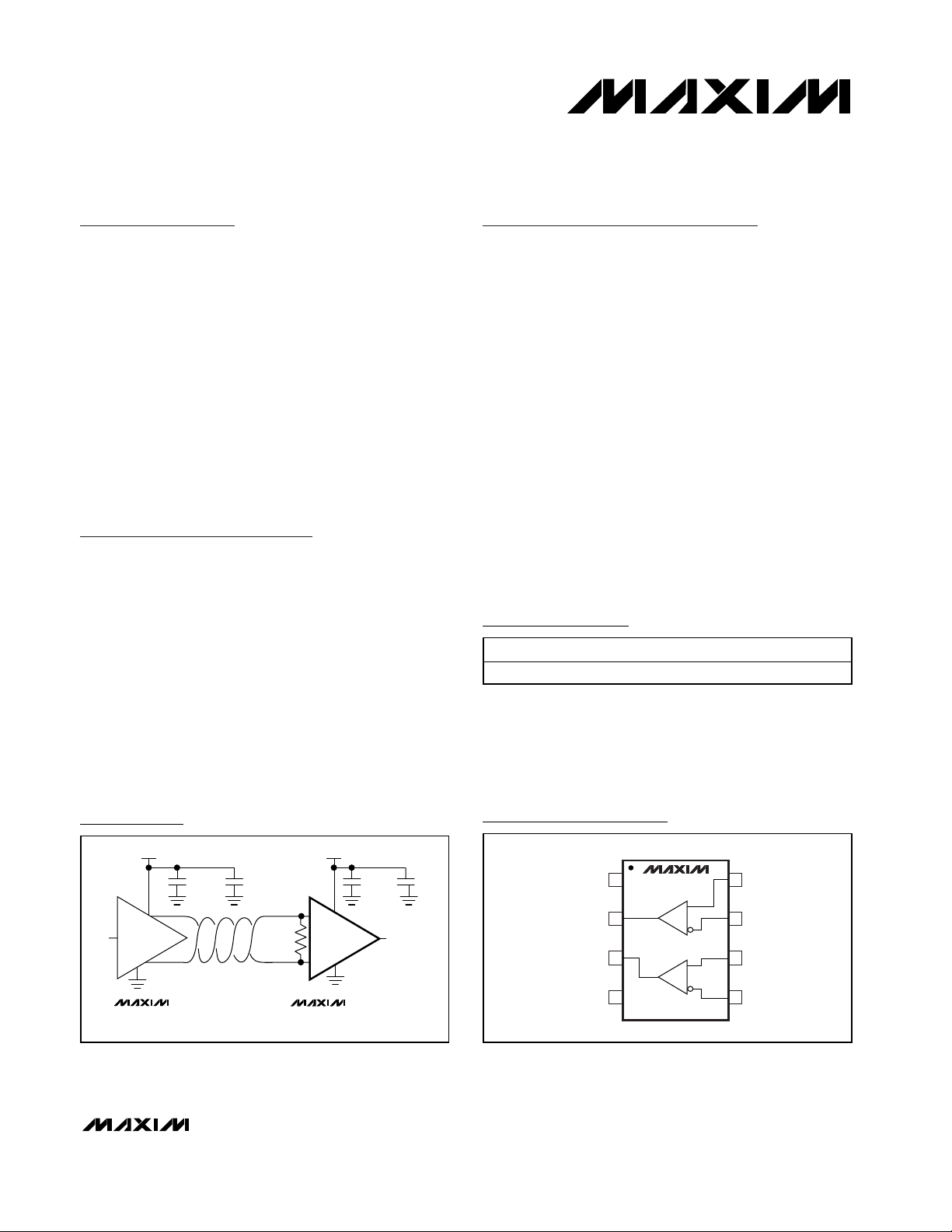
Typical Operating Circuit
19-2274; Rev 0; 1/02
For pricing, delivery, and ordering information, please contact Maxim/Dallas Direct! at
1-888-629-4642, or visit Maxim’s website at www.maxim-ic.com.
Pin Configuration
PART TEMP RANGE PIN-PACKAGE
MAX9159ESA -40°C to +85°C 8 SO
MAX9159
SO
TOP VIEW
1
V
CC
2
2Y
3
4
871A
6
5
1B1Y
2A
2BGND
Page 2
MAX9159
Dual LVDS Line Receiver
2 _______________________________________________________________________________________
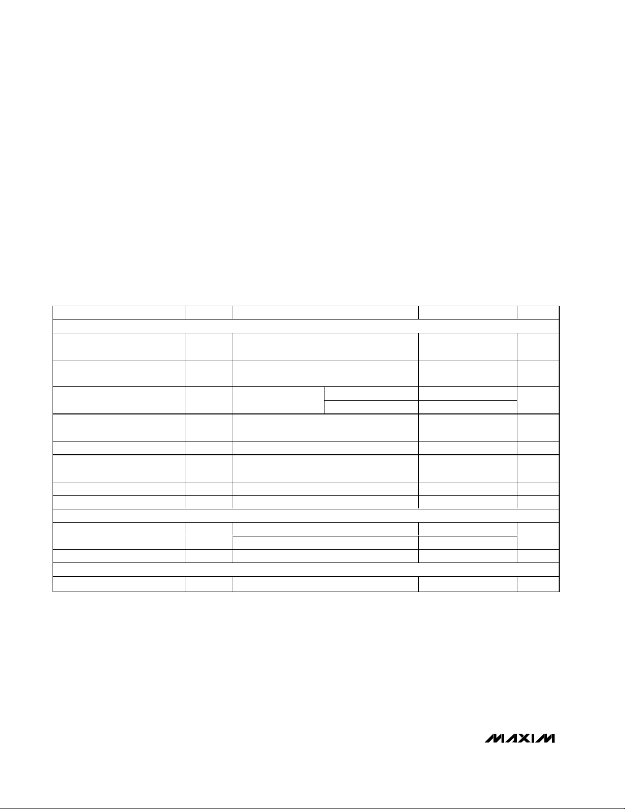
ABSOLUTE MAXIMUM RATINGS
ELECTRICAL CHARACTERISTICS
(VCC= 3.0V to 3.6V, differential input voltage |VID| = 0.1V to 0.6V, common-mode input voltage VCM= |VID/2| to 2.4V - |VID/2|, TA=
-40°C to +85°C. Typical values are at V
CC
= 3.3V, TA= +25°C, unless otherwise noted.) (Notes 1 and 2)
Stresses beyond those listed under “Absolute Maximum Ratings” may cause permanent damage to the device. These are stress ratings only, and functional
operation of the device at these or any other conditions beyond those indicated in the operational sections of the specifications is not implied. Exposure to
absolute maximum rating conditions for extended periods may affect device reliability.
VCCto GND..............................................................-0.5V to +4V
1A, 1B, 2A, 2B to GND ............................................-0.5V to +4V
Y1, Y2 to GND ............................................-0.5V to (VCC+ 0.5V)
Continuous Power Dissipation ................................(TA= +70°C)
8-Pin SO (derate 5.88mW/°C above +70°C)................471mW
Maximum Junction Temperature .....................................+150°C
Operating Temperature Range ...........................-40°C to +85°C
Storage Temperature Range .............................-65°C to +150°C
ESD Protection LVDS Inputs (1A, 1B, 2A, 2B)
Human Body Model ........................................................±8kV
Lead Temperature (soldering, 10s) .................................+300°C
)
LVDS INPUTS (1A, 1B, 2A, 2B)
Differential Input High
Threshold
Differential Input Low
Threshold
Input Current I
Input Current with Differential
Input
Power-Off Input Current I
Power-Off Input Current
with Differential Input
Input Resistor 1 R
Input Resistor 2 R
LVTTL OUTPUTS (Y1, Y2)
Output High Voltage V
Output Low Voltage V
SUPPLY
Supply Current I
PARAMETER SYMBOL CONDITIONS MIN TYP MAX UNITS
V
TH
V
TL
_A or _B inputs
I
I
ID
I(OFF)
I
ID(OFF
IN1
IN2
OH
OL
CC
0.1V ≤ |V
VCC = 0, VIN = 3.6V; _A or _B inputs 2.3 20 µA
0.1V ≤ |V
VCC = 0 or 3.6V, Figure 1 35 kΩ
VCC = 0 or 3.6V, Figure 1 157 kΩ
IOH = -8mA 2.4 3.14
IOH = -4mA 2.8 3.2
IOL = 8mA 0.19 0.4 V
No load 5.7 10 mA
≤ 0.6V; _A or _B inputs -20 20 µA
ID|
≤ 0.6V, VCC = 0; _A or _B inputs -15 15 µA
ID|
100 mV
-100 mV
VIN = 0 -1.0 -2.3 -20
V
= 2.4V -0.3 -0.67
IN
µA
V
Page 3
MAX9159
Dual LVDS Line Receiver
_______________________________________________________________________________________ 3
Note 1: Maximum and minimum limits over temperature are guaranteed by design and characterization. Devices are production
tested at T
A
= +25°C.
Note 2: Current into a pin is defined as positive. Current out of a pin is defined as negative. All voltages are referenced to ground,
except V
TH
, VTL, and VID.
Note 3: AC parameters are guaranteed by design and characterization.
Note 4: C
L
includes scope probe and test jig capacitance.
Note 5: All input pulses are supplied by a generator having the following characteristics: t
R
or tF≤ 1ns, pulse repetition rate (PRR) =
50Mpps, pulse width = 10 ±0.2ns.
Note 6: t
SK(O)
is the skew between specified outputs of a single device with all driving inputs connected together and the outputs
switching in the same direction while driving identical specified loads.
Note 7: t
SK(PP)
is the magnitude of the difference in propagation delay times between any specified terminals of two devices when
both devices operate with the same supply voltages, same temperature, and have identical packages and test circuits.
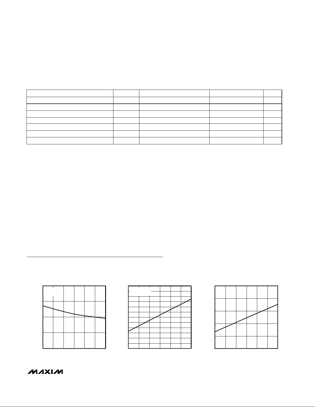
SWITCHING CHARACTERISTICS
(VCC= 3.0V to 3.6V, differential input voltage |VID| = 0.1V to 0.6V, common-mode input voltage VCM= |VID/2| to 2.4V - |VID/2|, CL=
10pF, T
A
= -40°C to +85°C. Typical values are at VCC= 3.3V, TA= +25°C, unless otherwise noted.) (Figures 2 and 3) (Notes 3, 4,
Typical Operating Characteristics
(VCC= 3.3V, |VID| = 200mV, VCM= 1.2V, fIN= 200MHz, CL= 10pF, TA= +25°C, unless otherwise noted.)
Propagation Delay High to Low t
Propagation Delay Low to High t
Pulse Skew | t
Channel-to-Channel Output Skew (Note 6) t
Part-to-Part Skew (Note 7) t
Output Signal Rise Time (20% to 80%) t
Output Signal Fall Time (80% to 20%) t
PARAMETER SYMBOL CONDITIONS MIN TYP MAX UNITS
PHL
PLH
- t
PHL
|t
PLH
SK(P)
SK(O)
SK(PP)
R
F
1.5 2.2 3 ns
1.5 2.13 3 ns
0.07 0.4 ns
0.03 0.3 ns
1ns
0.40 0.8 ns
0.42 0.8 ns
OUTPUT LOW VOLTAGE
vs. SUPPLY VOLTAGE
200
OUTPUT
SINKING 8mA
195
190
185
OUTPUT LOW VOLTAGE (mV)
180
3.0 3.33.1 3.2 3.4 3.5 3.6
SUPPLY VOLTAGE (V)
3.7
3.6
3.5
MAX9159 toc01
3.4
3.3
3.2
3.1
3.0
2.9
OUTPUT HIGH VOLTAGE (V)
2.8
2.7
2.6
2.5
OUTPUT HIGH VOLTAGE
vs. SUPPLY VOLTAGE
OUTPUT
SOURCING 8mA
3.0 3.23.1 3.3 3.4 3.5 3.6
SUPPLY VOLTAGE (V)
100
MAX9159 toc02
90
80
70
SHORT-CIRCUIT CURRENT (mA)
60
50
3.0 3.23.1 3.3 3.4 3.5 3.6
CURRENT vs. SUPPLY VOLTAGE
OUTPUT SHORT-CIRCUIT
MAX9159 toc03
SUPPLY VOLTAGE (V)
Page 4

MAX9159
Dual LVDS Line Receiver
4 _______________________________________________________________________________________
Typical Operating Characteristics (continued)
(VCC= 3.3V, |VID| = 200mV, VCM= 1.2V, fIN= 200MHz, CL= 10pF, TA= +25°C, unless otherwise noted.)
DIFFERENTIAL INPUT THRESHOLD
VOLTAGE vs. SUPPLY VOLTAGE
0
-0.5
-1.0
-1.5
-2.0
-2.5
-3.0
-3.5
-4.0
DIFFERENTIAL INPUT THRESHOLD (mV)
-4.5
-5.0
3.0 3.23.1 3.3 3.4 3.5 3.6
V
TH
SUPPLY VOLTAGE (V)
PROPAGATION DELAY
vs. SUPPLY VOLTAGE
2.4
MAX9159 toc04
V
TL
SUPPLY CURRENT vs. FREQUENCY
40
35
30
25
20
15
SUPPLY CURRENT (mA)
10
5
0
0.01 0.1 1 10 100 1000
TWO CHANNELS
SWITCHING
ONE CHANNEL
SWITCHING
FREQUENCY (MHz)
PROPAGATION DELAY vs. TEMPERATURE
2.5
MAX9159 toc05
SUPPLY CURRENT (mA)
150
SUPPLY CURRENT vs. TEMPERATURE
8
fIN = 1MHz
BOTH CHANNELS
SWITCHING
7
6
5
4
3
-40 10-15 35 60 85
TEMPERATURE (°C)
PULSE SKEW vs. SUPPLY VOLTAGE
MAX9159 toc06
2.3
t
PHL
2.2
t
PROPAGATION DELAY (ns)
2.1
2.0
3.0 3.33.1 3.2 3.4 3.5 3.6
PLH
SUPPLY VOLTAGE (V)
PULSE SKEW vs. TEMPERATURE
100
90
80
70
60
50
PULSE SKEW (ps)
40
30
20
-40 -15 10 35 60 85
TEMPERATURE (°C)
2.4
MAX9159 toc07
2.3
2.2
2.1
2.0
PROPAGATION DELAY (ns)
1.9
1.8
-40 10-15 35 60 85
PROPAGATION DELAY vs. DIFFERENTIAL
2.6
2.5
MAX9159 toc10
2.4
2.3
2.2
PROPAGATION DELAY (ns)
2.1
2.0
t
PHL
t
PLH
TEMPERATURE (°C)
INPUT VOLTAGE
t
PHL
t
PLH
0 2500
1000500 1500 2000
DIFFERENTIAL INPUT VOLTAGE (mV)
125
MAX9159 toc08
100
75
PULSE SKEW (ps)
50
25
0
3.0 3.2 3.33.1 3.4 3.5 3.6
2.6
2.5
MAX9159 toc11
2.4
2.3
2.2
PROPAGATION DELAY (ns)
2.1
2.0
SUPPLY VOLTAGE (V)
PROPAGATION DELAY
vs. COMMON-MODE VOLTAGE
t
PHL
t
PLH
0 1.0 1.50.5 2.0 2.5 3.0
COMMON-MODE VOLTAGE (V)
MAX9159 toc09
MAX9159 toc12
Page 5

MAX9159
Dual LVDS Line Receiver
_______________________________________________________________________________________ 5
Typical Operating Characteristics (continued)
(VCC= 3.3V, |VID| = 200mV, VCM= 1.2V, fIN= 200MHz, CL= 10pF, TA= +25°C, unless otherwise noted.)
Detailed Description
LVDS is intended for point-to-point communication over
a controlled-impedance medium as defined by the
ANSI TIA/EIA-644 and IEEE 1596.3 standards. LVDS
uses a lower voltage swing than other common communication standards, achieving higher data rates with
reduced power consumption, while reducing EMI
emissions and system susceptibility to noise.
The MAX9159 is a dual LVDS line receiver ideal for
applications requiring high data rates, low power, and
low noise. The device accepts an LVDS input and
translates it to an LVTTL output. The receiver detects
differential signals as low as 100mV and as high as
0.6V within an input voltage range of 0 to 2.4V.
The 250mV to 450mV differential output of an LVDS driver is nominally centered around a 1.25V offset. This
offset, coupled with the receiver’s 0 to 2.4V input voltage range, allows an approximate ±1V shift in the signal (as seen by the receiver). This allows for a
difference in ground references of the driver and the
receiver, the common-mode effects of coupled noise,
or both. The LVDS standards specify an input voltage
range of 0 to 2.4V referenced to receiver ground.
Fail-Safe
The fail-safe feature of the MAX9159 sets the output
high and reduces supply current when:
• Inputs are open.
• Inputs are undriven and shorted.
• Inputs are undriven and terminated.
A fail-safe circuit is important because under these
conditions, noise at the input may switch the receiver
and it may appear to the system that data is being
received. Open or undriven terminated input conditions
can occur when a cable is disconnected or cut, or
when an LVDS driver output is in high impedance. A
short condition can occur because of a cable failure.
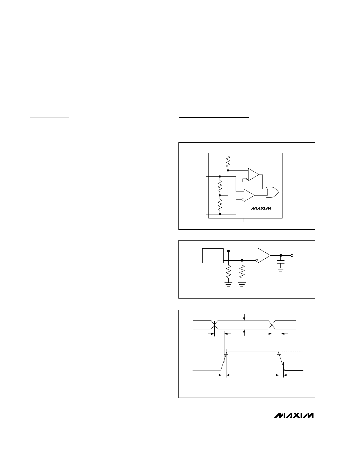
The fail-safe input network (Figure 1) samples the input
common-mode voltage and compares it to V
CC
- 0.3V
(nominal). When the input is driven to levels specified in
the LVDS standards, the input common-mode voltage is
less than VCC- 0.3V and the fail-safe circuit is not acti-
Pin Description
PROPAGATION DELAY
TRANSITION TIME vs. TEMPERATURE
0.6
0.5
t
F
0.4
TRANSITION TIME (ns)
0.3
0.2
-40 10-15 35 60 85
PIN NAME FUNCTION
t
R
TEMPERATURE (°C)
3.6
3.4
MAX9159 toc13
3.2
3.0
2.8
2.6
PROPAGATION DELAY (ns)
2.4
2.2
2.0
1VCCPower Supply
2 1Y Channel 1 Output
3 2Y Channel 2 Output
4 GND Ground
5 2B Channel 2 Inverting Differential Input
6 2A Channel 2 Noninverting Differential Input
7 1B Channel 1 Inverting Differential Input
8 1A Channel 1 Noninverting Differential Input
vs. LOAD CAPACITANCE
t
PHL
t
PLH
10 20 2515 30 35 40 45 50
LOAD CAPACITANCE (pF)
2.2
2.0
MAX9159 toc14
1.8
1.6
1.4
1.2
1.0
0.8
TRANSITION TIME (ns)
0.6
0.4
0.2
0
10 20 2515 30 35 40 45 50
TRANSITION TIME
vs. LOAD CAPACITANCE
t
F
t
R
LOAD CAPACITANCE (pF)
MAX9159 toc15
Page 6
MAX9159
Dual LVDS Line Receiver
6 _______________________________________________________________________________________
vated. If the inputs are open or if the inputs are undriven
and shorted or undriven and parallel terminated, there is
no input current. In this case, a pullup resistor in the failsafe circuit pulls both inputs above VCC- 0.3V, activating
the fail-safe circuit and forcing the output high.
Applications Information
Power-Supply Bypassing
Bypass VCCwith high-frequency surface-mount ceramic 0.1µF and 0.001µF capacitors in parallel as close to
the device as possible, with the smaller value capacitor
closest to the device.
Differential Traces
Input trace characteristics affect the performance of the
MAX9159. Use controlled-impedance PC board traces,
typically 100Ω. Match the termination resistor to this
characteristic impedance. Eliminate reflections and
ensure that noise couples as common mode by running
the differential traces close together. Reduce skew by
matching the electrical length of the traces. Excessive
skew can result in a degradation of magnetic field cancellation. Input differential signals should be routed
close to each other to cancel their external magnetic
field. Maintain a constant distance between the differential traces to avoid discontinuities in differential
impedance. Minimize the number of vias to further prevent impedance discontinuities.
Cables and Connectors
Transmission media should typically have a controlled
differential impedance of 100Ω. Use cables and connectors that have matched differential impedance to
minimize impedance discontinuities. Avoid the use of
unbalanced cables such as ribbon or simple coaxial
cable. Balanced cables such as twisted pair offer
superior signal quality and tend to generate less EMI
due to canceling effects. Balanced cables tend to pick
up noise as common mode, which is rejected by the
LVDS receiver.
Termination
In point-to-point connections, the MAX9159 requires an
external termination resistor. The termination resistor
should match the differential impedance of the transmission line. Termination resistance is typically 100Ω, but
may range between 90Ω to 132Ω, depending on the
characteristic impedance of the transmission medium.
When using the MAX9159, minimize the distance
between the input termination resistor and the
MAX9159 inputs. Use 1% surface-mount resistors.
Board Layout
For LVDS applications, use a four-layer PC board with
separate layers for power, ground, and input/output. To
minimize crosstalk, do not run the output in parallel with
the inputs.
Chip Information
TRANSISTOR COUNT: 461
PROCESS: CMOS
Figure 1. Input Fail-Safe Network
Figure 2. Propagation Delay and Transition-Time Test Circuit
Figure 3. Propagation Delay and Transition-Time Waveforms
V
CC
R
IN2
_A
80%
t
R
= (V_A + V_B) / 2
CM
ID
VCC - 0.3V
GND
V
ID
= (V_A) - (V_B)
MAX9159
_A
_B
MAX9159
80%
_Y
_Y
C
L
1.4V
= 0
V
ID
t
PHL
1V
V
OH
1.4V
V
OL
t
F
R
IN1
R
IN1
_B
PULSE
GENERATOR
*50Ω *50Ω
*50Ω REQUIRED FOR PULSE GENERATOR.
V
_B
V
_A
V_
Y
COMMON-MODE VOLTAGE: V
DIFFERENTIAL INPUT VOLTAGE: V
VID = 0
t
PLH
1.4V
20% 20%
Page 7

MAX9159
Dual LVDS Line Receiver
Maxim cannot assume responsibility for use of any circuitry other than circuitry entirely embodied in a Maxim product. No circuit patent licenses are
implied. Maxim reserves the right to change the circuitry and specifications without notice at any time.
Maxim Integrated Products, 120 San Gabriel Drive, Sunnyvale, CA 94086 408-737-7600 _____________________ 7
© 2002 Maxim Integrated Products Printed USA is a registered trademark of Maxim Integrated Products.
Package Information
SOICN.EPS
 Loading...