

Page 1
General Description
The MAX9157 is a quad bus LVDS (BLVDS) transceiver
for heavily loaded, half-duplex multipoint buses. Small
32-pin QFN and TQFP packages and flow-through
pinouts allow the transceiver to be placed near the connector for the shortest possible stub length. The
MAX9157 drives LVDS levels into a 27Ω load (double
terminated, heavily loaded LVDS bus) at up to
200Mbps. An input fail-safe circuit ensures the receiver
output is high when the differential inputs are open, or
undriven and shorted, or undriven and terminated. The
MAX9157 differential inputs feature 52mV hysteresis for
greater immunity to bus noise and reflections. The
MAX9157 operates from a single 3.3V supply, consuming 80.9mA supply current with drivers enabled, and
22.7mA with drivers disabled.
The MAX9157’s high-impedance I/Os (except for
receiver outputs) when VCC= 0 or open, combined
with glitch-free power-up and power-down, allow hot
swapping of cards in multicard bus systems; 7.2pF
(max) BLVDS I/O capacitances minimize bus loading.
The MAX9157 is offered in 5mm ✕ 5mm 32-pin QFN and
TQFP packages. The MAX9157 is fully specified for the
-40°C to +85°C extended temperature range. Refer to
the MAX9129 data sheet for a quad BLVDS driver, ideal
for dual multipoint full-duplex buses.
Applications
Features
♦ 32-TQFP and Space-Saving 32-QFN Packages
♦ 52mV LVDS Input Hysteresis
♦ 1ns (min) Transition Time (0% to 100%) Minimizes
Reflections
♦ Guaranteed 7.2pF (max) Bus Load Capacitance
♦ Glitch-Free Power-Up and Power-Down
♦ Hot-Swappable, High-Impedance I/O with V
CC
= 0
or Open
♦ Guaranteed 200Mbps Driver Data Rate
♦ Fail-Safe Circuit
♦ Flow-Through Pinout
MAX9157
Quad Bus LVDS Transceiver
________________________________________________________________ Maxim Integrated Products 1
Ordering Information
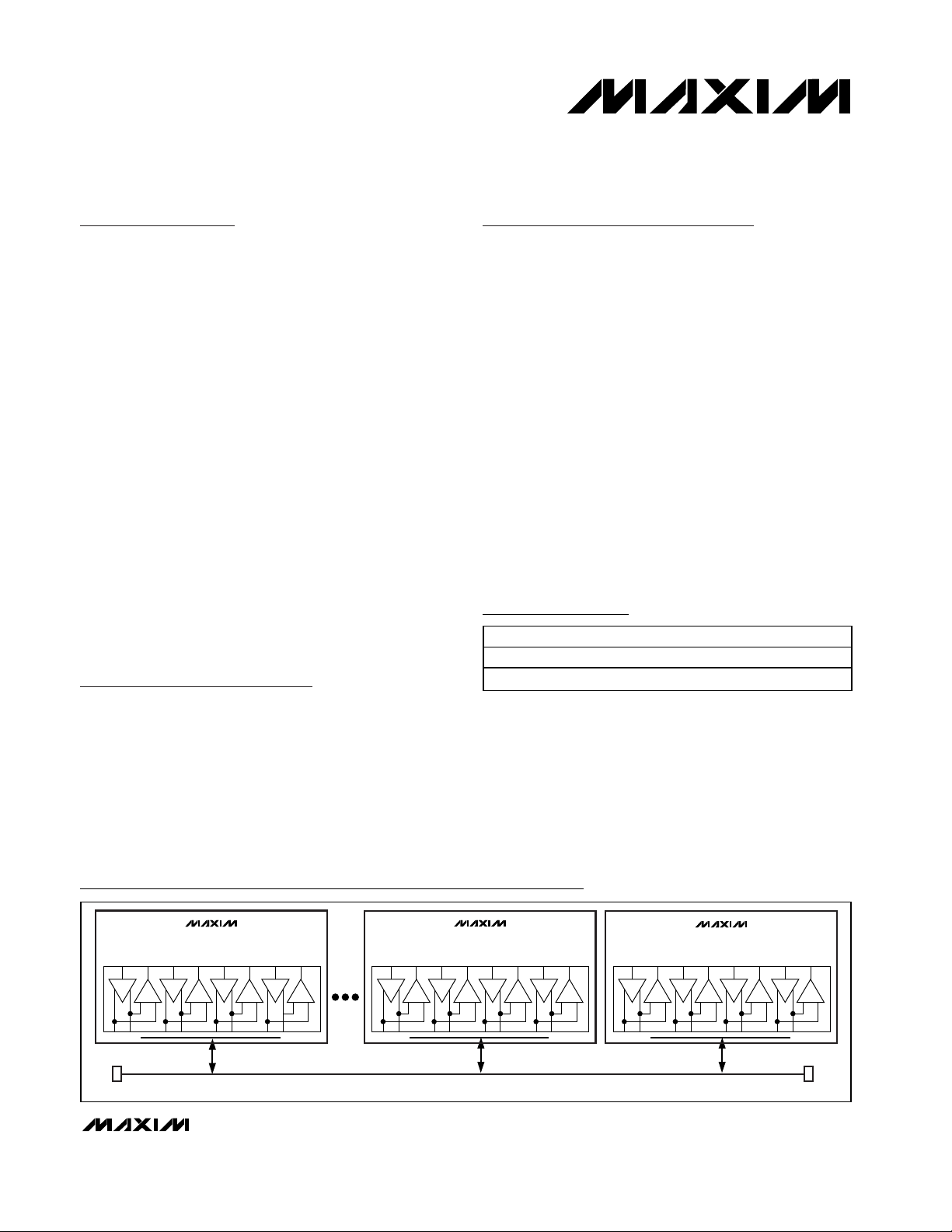
CARD 1 CARD 15 CARD 16
1in CARD
SPACING
Rt = 54Ω Rt = 54Ω
MAX9157
MAX9157
MAX9157
Typical Operating Circuit
19-2287; Rev 0; 1/02
For pricing, delivery, and ordering information, please contact Maxim/Dallas Direct! at
1-888-629-4642, or visit Maxim’s website at www.maxim-ic.com.
Pin Configurations appear at end of data sheet.
Functional Diagram appears at end of data sheet.
Add/Drop Muxes
Digital Cross-Connects
Network
Switches/Routers
Cellular Phone Base
Stations
DSLAMs
Multipoint Buses
PART TEMP RANGE PIN-PACKAGE
MAX9157EGJ -40°C to +85°C 32 QFN (5mm
MAX9157EHJ -40°C to +85°C 32 TQFP (5mm ✕ 5mm)
✕ 5mm)
Page 2
MAX9157
Quad Bus LVDS Transceiver
2 _______________________________________________________________________________________
ABSOLUTE MAXIMUM RATINGS
DC ELECTRICAL CHARACTERISTICS
(VCC= 3.0V to 3.6V, RL= 27Ω ±1%, differential input voltage |VID| = 0.1V to VCC, input common-mode voltage VCM= 0.05V to 2.4V,
input voltage range = 0 to V
CC
, DE_ = high, RE_ = low, TA= -40°C to +85°C, unless otherwise noted. Typical values are at VCC=
3.3V, |V
ID
| = 0.2V, VCM= 1.2V, and TA= +25°C.) (Notes 1 and 2)
Stresses beyond those listed under “Absolute Maximum Ratings” may cause permanent damage to the device. These are stress ratings only, and functional
operation of the device at these or any other conditions beyond those indicated in the operational sections of the specifications is not implied. Exposure to
absolute maximum rating conditions for extended periods may affect device reliability.
VCC, AVCCto GND................................................-0.3V to +4.0V
DO_+/RIN_+, DO_-/RIN_-, to GND .......................-0.3V to +4.0V
DIN_, DE_, RE_ to GND.........................................-0.3V to +4.0V
RO_ to GND................................................-0.3V to (V
CC
+ 0.3V)
AGND to GND .......................................................-0.3V to +0.3V
Short-Circuit Duration (DO_+/RIN_+, DO_-/RIN_-) ....Continuous
Continuous Power Dissipation (T
A
= +70°C)
MAX9157EGJ (derate 21.2mW/°C above +70°C) .....1702mW
MAX9157EHJ (derate 11.1mW/°C above +70°C).........889mW
Storage Temperature Range .............................-65°C to +150°C
Maximum Junction Temperature .....................................+150°C
Operating Temperature Range ...........................-40°C to +85°C
ESD Protection
Human Body Model (DO_+/RIN_+, DO_-/RIN_-).............±4kV
Lead Temperature (soldering, 10s) .................................+300°C
PARAMETER SYMBOL CONDITIONS MIN TYP MAX UNITS
BLVDS (DO_+/RIN_+, DO_-/RIN_-)
Differential Input High Threshold V
Differential Input Low Threshold V
Threshold Hysteresis (Note 3) V
Input Current I
Input Resistance
Power-Off Input Current
Differential Output Voltage V
Change in Magnitude of VOD for
Complementary Output States
Offset Voltage V
Change in Magnitude of VOS for
Complementary Output States
Output High Voltage V
Output Low Voltage V
Output Short-Circuit Current I
DE_ = low 26 100 mV
TH
DE_ = low -100 -26 mV
TL
HYST
IN+
R
R
I
INO+
I
INO- 0.6V < V
OD
∆V
OS
∆V
OH
DE_ = low
0.1V ≤VID≤ 0.6V, DE_ = low -15 ±1.8 15 µA
, I
IN-
0.6V < VID≤ 1.2V, DE_ = low -20 ±2.5 20 µA
V
IN1
IN2
,
= 3.6V, 0 or open, Figure 1 53 kΩ
CC
V
= 3.6V, 0 or open, Figure 1 148 kΩ
CC
0.1V ≤ VID≤ 0.6V, V
≤ 1.2V, V
ID
Figure 2 250 405 460 mV
Figure 2 1 25 mV
OD
Figure 2 1.185 1.302 1.435 V
Figure 2 3.3 25 mV
OS
Figure 2 1.505 1.6 V
Figure 2 0.9 1.099 V
OL
DIN_ = high, DO_+/RIN_+ = 0 or
V
, DO_-/RIN_- = 0 or V
OS
CC
DIN_ = low, DO_-/RIN_- = 0 or
V
, DO_+/RIN_+ = 0 or V
CC
TA = +25°C, VCC = 3.3V,
= 1.2V
V
CM
12 26 43
Full operating range 9 26 78
= 0 or open -15 ±0.9 15 µA
CC
= 0 or open -20 ±1.8 20 µA
CC
CC
CC
-30 -14.8 30
-30 -14.8 30
mV
mA
Page 3
MAX9157
Quad Bus LVDS Transceiver
_______________________________________________________________________________________ 3
DC ELECTRICAL CHARACTERISTICS (continued)
(VCC= 3.0V to 3.6V, RL= 27Ω ±1%, differential input voltage |VID| = 0.1V to VCC, input common-mode voltage VCM= 0.05V to 2.4V,
input voltage range = 0 to V
CC
, DE_ = high, RE_ = low, TA= -40°C to +85°C, unless otherwise noted. Typical values are at VCC=
3.3V, |V
ID
| = 0.2V, VCM= 1.2V, and TA= +25°C.) (Notes 1 and 2)
_
PARAMETER SYMBOL CONDITIONS MIN TYP MAX UNITS
Differential Output Short-Circuit
Current (Note 3)
Capacitance at Bus Pins
(Note 3)
LVCMOS/LVTTL OUTPUTS (RO_)
Output High Voltage V
Output Low Voltage V
Dynamic Output Current I
Output Short-Circuit Current
(Note 4)
Output High-Impedance Current I
Capacitance at Receiver Output
(Note 3)
LVCMOS/LVTTL INPUTS (DIN, DE, RE)
Input High Voltage V
Input Low Voltage V
Input Current I
Power-Off Input Current I
SUPPLY
Supply Current Drivers and
Receivers Enabled
Supply Current Drivers Enabled
and Receivers Disabled
Supply Current Drivers Disabled
and Receivers Enabled
Supply Current Drivers Disabled
and Receivers Disabled
I
OSD
C
OUTPUT
OD
I
OS
OZ
C
OUTPUT
INO
I
CC
I
CCD
I
CCR
I
CCZ
OH
OL
IN
DIN_ = high or low, VOD = 0 14.8 30 mA
Capacitance from DO_+/RIN_+ or
DO_-/RIN_- to GND, V
IOH = -4.0mA,
DE_ = low
= 3.6V or 0
CC
Open, undriven short, or
undriven 27Ω parallel
termination
VID = 100mV
-
CC
VCC -
0.172
-
VCC -
0.172
V
0.3
V
CC
0.3
IOL = 4.0mA, VID = -100mV, DE_ = low 0.179 0.25 V
VID = 100mV, V
VID = -100mV, V
VID = 100mV, V
RE_ = high, V
= VCC - 1.0V, DE_ = low -15 -22.7 mA
RO
= 1.0V, DE_ = low 12 19.9 mA
RO_
= 0, DE_ = low -52 -130 mA
RO_
RO
= 0 or V
CC
-10 0.1 +10 µA
Capacitance from RO_ to GND, VCC = 3.6V
or 0
IH
IL
V
, V
, V
DE
RE_
_
V
, V
DE
RE_
_
= high or low -20 ±9.2 20 µA
DIN_
, V
DIN_
= 3.6V or 0, V
CC
= 0
or open
2.0 1.825 V
GND 1.315 0.8 V
-20 ±2.4 20 µA
DE_ = high, RE_ = low, RL = 27Ω 80.9 95 mA
DE_ = high, RE_ = high, RL = 27Ω 80.9 95 mA
DE_ = low, RE_ = low 22.7 30 mA
DE_ = low, RE_ = high 22.7 30 mA
7.2 pF
4.5 pF
CC
V
V
Page 4
MAX9157
Quad Bus LVDS Transceiver
4 _______________________________________________________________________________________
AC ELECTRICAL CHARACTERISTICS
(VCC= 3.0V to 3.6V, RL= 27Ω ±1%, differential input voltage |VID| = 0.2V to VCC, input frequency to LVDS inputs = 85MHz, input frequency to LVCMOS/LVTTL inputs = 100MHz, LVCMOS/LVTTL inputs = 0 to 3V with 2ns (10% to 90%) transition times. Differential input
voltage transition time = 1ns (20% to 80%). Input common-mode voltage V
CM
= 1.2V to 1.8V, DE_ = high, RE_ = low, TA= -40°C to
+85°C, unless otherwise noted. Typical values are at V
CC
= 3.3V, |VID| = 0.2V, VCM= 1.2V, and TA= +25°C.) (Notes 3 and 5)
PARAMETER SYMBOL CONDITIONS MIN TYP MAX UNITS
DRIVER
Differential Propagation Delay
High to Low
Differential Propagation Delay
Low to High
Differential Skew | t
PHLD
- t
PLHD
(Note 6)
Channel-to-Channel Skew
(Note 7)
Chip-to-Chip Skew (Note 8) t
Chip-to-Chip Skew (Note 9) T
Rise Time t
Fall Time t
Disable Time High to Z t
Disable Time Low to Z t
Enable Time Z to High t
Enable Time Z to Low t
Maximum Operating Frequency
(Note 10)
t
PHLD
t
PLHD
|
t
SKD1
t
CCSK
SKD2
SKD3
TLH
THL
PHZ
PLZ
PZH
PZL
f
MAX
RE_ = high, CL = 10pF,
Figures 3, 4
RE_ = high, CL = 10pF,
Figures 3, 4
RE_ = high, CL = 10pF, Figures 3, 4 33 160 ps
RE_ = high, CL = 10pF, Figures 3, 4 58 300 ps
RE_ = high, CL = 10pF, Figures 3, 4 0.38 0.8 ns
RE_ = high, CL = 10pF, Figures 3, 4 1.3 ns
RE_ = high, CL = 10pF,
Figures 3, 4
RE_ = high, CL = 10pF,
Figures 3, 4
RE_ = high, CL = 10pF,
Figures 5, 6
RE_ = high, CL = 10pF,
Figures 5, 6
RE_ = high, CL = 10pF,
Figures 5, 6
RE_ = high, CL = 10pF,
Figures 5, 6
RE_ = high, CL = 10pF, Figures 5, 6 100 MHz
RECEIVER
Differential Propagation Delay
High to Low
Differential Propagation Delay
Low to High
Differential Skew | t
| (Note 6)
t
PLHD
PHLD
-
Channel-to-Channel Skew
(Note 7)
Chip-to-Chip Skew (Note 8) t
Chip-to-Chip Skew (Note 9) t
Rise Time t
t
PHLD
t
PLHD
t
SKD1
t
CCSK
SKD2
SKD3
TLH
DE_ = low, Figures 7, 8;
C
=15pF
L
DE_ = low, Figures 7, 8;
=15pF
C
L
DE_ = low, Figures 7, 8; C
DE_ = low, Figures 7, 8; C
DE_ = low, Figures 7, 8; CL =15pF 0.7 1.7 ns
DE_ = low, Figures 7, 8; CL =15pF 0.7 1.7 ns
DE_ = low, Figures 7, 8; C
MAX9157EGJ 1.2 1.96 2.5
MAX9157EHJ 1.1 1.87 2.4
MAX9157EGJ 1.2 1.94 2.5
MAX9157EHJ 1.1 1.84 2.4
MAX9157EGJ 0.6 1.13 1.4
MAX9157EHJ 0.6 1.07 1.4
MAX9157EGJ 0.6 1.16 1.4
MAX9157EHJ 0.6 1.11 1.4
MAX9157EGJ 6.79 8
MAX9157EHJ 6.79 8
MAX9157EGJ 3.16 8
MAX9157EHJ 3.48 8
MAX9157EGJ 4.67 7
MAX9157EHJ 4.71 7
MAX9157EGJ 4.36 7
MAX9157EHJ 4.39 7
MAX9157EGJ 1.8 2.58 4.1
MAX9157EHJ 1.8 2.61 4.1
MAX9157EGJ 1.8 2.49 4.1
MAX9157EHJ 1.8 2.52 4.1
= 15pF 90 450 ps
L
= 15pF 131 580 ps
L
= 15pF 0.5 1.1 1.6 ns
L
ns
ns
ns
ns
ns
ns
ns
ns
ns
ns
Page 5
MAX9157
Quad Bus LVDS Transceiver
_______________________________________________________________________________________ 5
AC ELECTRICAL CHARACTERISTICS (continued)
(VCC= 3.0V to 3.6V, RL= 27Ω ±1%, differential input voltage |VID| = 0.2V to VCC, input frequency to LVDS inputs = 85MHz, input frequency to LVCMOS/LVTTL inputs = 100MHz, LVCMOS/LVTTL inputs = 0 to 3V with 2ns (10% to 90%) transition times. Differential input
voltage transition time = 1ns (20% to 80%). Input common-mode voltage V
CM
= 1.2V to 1.8V, DE_ = high, RE_ = low, TA= -40°C to
+85°C, unless otherwise noted. Typical values are at V
CC
= 3.3V, |VID| = 0.2V, VCM= 1.2V, and TA= +25°C.) (Notes 3 and 5)
Note 1: Current into a pin is defined as positive. Current out of a pin is defined as negative. All voltages are referenced to ground
except V
TH
, VTL, VID, V
HYST
, VOD, and ∆VOD.
Note 2: Maximum and minimum limits over temperature are guaranteed by design and characterization. Devices are production
tested at T
A
= +25°C.
Note 3: Guaranteed by design and characterization.
Note 4: Short only one output at a time. Do not exceed the absolute maximum junction temperature specification.
Note 5: C
L
includes scope probe and test jig capacitance.
Note 6: t
SKD1
is the magnitude difference of differential propagation delays in a channel. t
SKD1
= | t
PHLD
- t
PLHD
|.
Note 7: t
CCSK
is the magnitude difference of the t
PLHD
or t
PHLD
of one channel and the t
PLHD
or t
PHLD
of any other channel on the
same part.
Note 8: t
SKD2
is the magnitude difference of any differential propagation delays between parts operating over rated conditions at
the same V
CC
and within 5°C of each other.
Note 9: t
SKD3
is the magnitude difference of any differential propagation delays between parts operating over rated conditions.
Note 10: Meets data sheet specifications while operating at minimum f
MAX
rating.
Typical Operating Characteristics
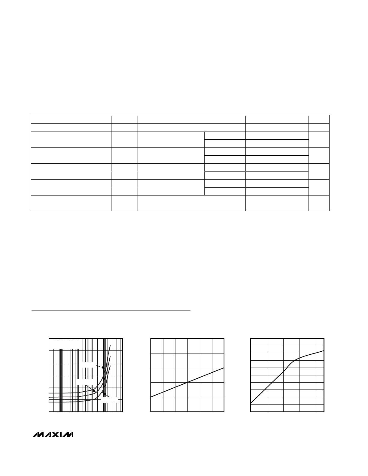
(VCC= 3.3V, RL= 27Ω, driver CL= 10pF, receiver CL= 15pF, |VID| = 200mV, VCM= 1.2V, fIN= 20MHz, TA= +25°C, unless otherwise noted.)
75
85
80
95
90
100
105
0.01 1000
SUPPLY CURRENT vs. FREQUENCY
MAX9157 toc01
FREQUENCY (MHz)
SUPPLY CURRENT (mA)
10.1 10 100
FOUR CHANNELS
DRIVEN
VCC = 3.6V
VCC = 3.3V
VCC = 3.0V
0.400
0.401
0.403
0.402
0.404
0.405
3.0 3.23.1 3.3 3.4 3.5 3.6
DIFFERENTIAL OUTPUT VOLTAGE
vs. SUPPLY VOLTAGE
MAX9157 toc02
SUPPLY VOLTAGE (V)
DIFFERENTIAL OUTPUT VOLTAGE (V)
0
0.6
0.4
0.2
0.8
1.0
1.2
1.4
1.6
1.8
2.0
15 45 75 105 135
DIFFERENTIAL OUTPUT VOLTAGE
vs. OUTPUT LOAD
MAX9157 toc03
OUTPUT LOAD (Ω)
DIFFERENTIAL OUTPUT VOLTAGE (V)
Fall Time t
Disable Time High to Z t
Disable Time Low to Z t
Enable Time Z to High t
Enable Time Z to Low t
Maximum Operating Frequency
(Note 10)
PARAMETER SYMBOL CONDITIONS MIN TYP MAX UNITS
THL
PHZ
PLZ
PZH
PZL
f
MAX
DE_ = low, Figures 7, 8; C
DE_ = low, RL = 500Ω, C
= 15pF, Figures 9, 10
DE_ = low, RL = 500Ω, C
= 15pF, Figures 9, 10
DE_ = low, RL = 500Ω, C
= 15pF, Figures 9, 10
DE_ = low, RL = 500Ω, C
= 15pF, Figures 9, 10
DE_ = low, CL = 15pF 85 MHz
= 15pF 0.7 1.2 1.8 ns
L
MAX9157EGJ 6.74 8
L
MAX9157EHJ 6.82 8
MAX9157EGJ 6.49 8
L
MAX9157EHJ 6.79 8
MAX9157EGJ 4.67 7
L
MAX9157EHJ 4.57 7
MAX9157EGJ 5.43 7
L
MAX9157EHJ 4.71 7
ns
ns
ns
ns
Page 6

MAX9157
Quad Bus LVDS Transceiver
6 _______________________________________________________________________________________
Typical Operating Characteristics (continued)
(VCC= 3.3V, RL= 27Ω, driver CL= 10pF, receiver CL= 15pF, |VID| = 200mV, VCM= 1.2V, fIN= 20MHz, TA= +25°C, unless otherwise noted.)
1.3
1.2
1.1
DRIVER TRANSITION TIME (ns)
1.0
1.20
1.15
1.10
1.05
1.00
DRIVER TRANSITION TIME (ns)
0.95
DRIVER TRANSITION TIME
vs. LOAD CAPACITANCE
t
THL
t
TLH
51510 20 25
LOAD CAPACITANCE (pF)
DRIVER TRANSITION TIME
vs. SUPPLY VOLTAGE
t
THL
t
TLH
MAX9157 toc04
MAX9157 toc06
DRIVER TRANSITION TIME
vs. TEMPERATURE
1.3
1.2
t
1.1
1.0
0.9
DRIVER TRANSITION TIME (ns)
0.8
0.7
-40 85
THL
t
TLH
10-15 35 60
TEMPERATURE (°C)
RECEIVER TRANSITION TIME
vs. LOAD CAPACITANCE
3.0
2.5
t
2.0
1.5
1.0
RECEIVER TRANSITION TIME (ns)
0.5
THL
t
TLH
MAX9157 toc05
MAX9157 toc07
0.90
3.0 3.2 3.33.1 3.4 3.5 3.6
SUPPLY VOLTAGE (V)
0
51510 20 25 30
LOAD CAPACITANCE (pF)
Page 7
MAX9157
Quad Bus LVDS Transceiver
_______________________________________________________________________________________ 7
Pin Description
*MAX9157EGJ only.
PIN NAME FUNCTION
1, 2, 22, 23, 24 N.C. No Connection. Not internally connected.
3VCCDigital Power Supply
4, 21 GND Digital Ground
5 RE34
6 DE34
7, 17 AGND Analog Ground
8, 19 AV
9 DO4-/RIN4- Channel 4 Inverting BLVDS Input/Output
10 DO4+/RIN4+ Channel 4 Noninverting BLVDS Input/Output
11 DO3-/RIN3- Channel 3 Inverting BLVDS Input/Output
12 DO3+/RIN3+ Channel 3 Noninverting BLVDS Input/Output
13 DO2-/RIN2- Channel 2 Inverting BLVDS Input/Output
14 DO2+/RIN2+ Channel 2 Noninverting BLVDS Input/Output
15 DO1-/RIN1- Channel 1 Inverting BLVDS Input/Output
16 DO1+/RIN1+ Channel 1 Noninverting BLVDS Input/Output
18 DE12
20 RE12
25 DIN1 Driver Channel 1 Input
26 RO1 Receiver Channel 1 Output
27 DIN2 Driver Channel 2 Input
28 RO2 Receiver Channel 2 Output
29 DIN3 Driver Channel 3 Input
30 RO3 Receiver Channel 3 Output
31 DIN4 Driver Channel 4 Input
32 RO4 Receiver Channel 4 Output
EP* EXPOSED PAD Exposed Pad. Solder exposed pad to GND.
CC
Receiver Channels 3 and 4 Enable (Enable Low). Drive RE34 low to enable receiver
channels 3 and 4.
Driver Channels 3 and 4 Enable (Enable High). Drive DE34 high to enable driver channels
3 and 4.
Analog Power Supply
Driver Channels 1 and 2 Enable (Enable High). Drive DE12 high to enable driver channels
1 and 2.
Receiver Channels 1 and 2 Enable (Enable Low). Drive RE12 low to enable receiver
channels 1 and 2.
Page 8

MAX9157
Detailed Description
The MAX9157 is a four-channel, 200Mbps, 3.3V BLVDS
transceiver in 32-lead TQFP and QFN packages, ideal
for driving heavily loaded multipoint buses, typically 16
to 20 cards plugged into a backplane. The MAX9157
receivers accept a differential input and have a fail-safe
input circuit. The devices detect differential signals as
low as 100mV and as high as VCC.
The MAX9157 driver outputs use a current-steering
configuration to generate a 9.25mA to 17mA output
current. This current-steering approach induces less
ground bounce and no shoot-through current, enhancing noise margin and system speed performance. The
outputs are short-circuit current limited.
The MAX9157 current-steering output requires a resistive load to terminate the signal and complete the transmission loop. Because the devices switch the direction
of current flow and not voltage levels, the output voltage swing is determined by the value of the termination
resistor multiplied by the output current. With a typical
15mA output current, the MAX9157 produces a 405mV
output voltage when driving a bus terminated with two
54Ω resistors (15mA ✕ 27Ω = 405mV). Logic states are
determined by the direction of current flow through the
termination resistor.
Fail-Safe Receiver Inputs
The fail-safe feature of the MAX9157 sets the output
high when the differential input is:
• Open
• Undriven and shorted
• Undriven and terminated
Without a fail-safe circuit, when the input is undriven,
noise at the input may switch the outputs and it may
appear to the system that data is being sent. Open or
undriven terminated input conditions can occur when a
cable is disconnected or cut, or when driver output is in
high impedance. A shorted input can occur because of
a cable failure.
When the input is driven with a differential signal with a
common-mode voltage of 0.05V to 2.4V, the fail-safe
circuit is not activated. If the input is open, undriven
and shorted, or undriven and parallel terminated, an
internal resistor in the fail-safe circuit pulls both inputs
above V
CC
- 0.3V, activating the fail-safe circuit and
forcing the outputs high (Figure 1).
Effect of Capacitive Loading
The characteristic impedance of a differential PC board
trace is uniformly reduced when equal capacitive loads
are attached at equal intervals (provided the transition
time of the signal being driven on the trace is longer
than the delay between loads). This kind of loading is
typical of multipoint buses where cards are attached at
1in or 0.8in intervals along the length of a backplane.
The reduction in characteristic impedance is approximated by the following formula:
Z
DIFF
-loaded = Z
DIFF
-unloaded ✕
SQRT [Co / (Co + N ✕ CL/ L)]
where:
Z
DIFF
-unloaded = unloaded differential characteristic
impedance
Co = unloaded trace capacitance (pF/unit length)
CL= value of each capacitive load (pF)
N = number of capacitive loads
L = trace length
For example, if Co = 2.5pF/in, CL= 10pF, N = 18, L =
18in, and Z
DIFF
-unloaded = 120Ω, the loaded differen-
tial impedance is:
Z
DIFF
-loaded = 120Ω ✕
SQRT [2.5pF / (2.5pF + 18 x 10pF / 18in)]
ZDIFF-loaded = 54Ω
In this example, capacitive loading reduces the characteristic impedance from 120Ω to 54Ω. The load seen by
Quad Bus LVDS Transceiver
8 _______________________________________________________________________________________
Figure 1. Internal Fail-Safe Circuit
V
CC
R
IN2
- 0.3V
V
CC
DO_+/RIN_+
R
D0_-/RIN_-
IN1
R
IN1
MAX9157
RO_
Page 9

a driver located on a card in the middle of the bus is
27Ω because the driver sees two 54Ω loads in parallel.
A typical LVDS driver (rated for a 100Ω load) would not
develop a large enough differential signal to be reliably
detected by an LVDS receiver. The MAX9157 BLVDS
drivers are designed and specified to drive a 27Ω load
to differential voltage levels of 250mV to 460mV. A standard LVDS receiver is able to detect this level of differential signal. Short extensions off the bus, called stubs,
contribute to capacitive loading. Keep stubs less than
1in for a good balance between ease of component
placement and good signal integrity.
The MAX9157 driver outputs are current-source drivers
and drive larger differential signal levels into loads
lighter than 27Ω and smaller levels into loads heavier
than 27Ω (see Typical Operating Characteristics
curves). To keep loading from reducing bus impedance
below the rated 27Ω load, PC board traces can be
designed for higher unloaded characteristic impedance.
Effect of Transition Times
For transition times (measured from 0% to 100%) shorter than the delay between capacitive loads, the loads
are seen as low-impedance discontinuities from which
the driven signal is reflected. Reflections add and subtract from the signal being driven and cause decreased
noise margin and jitter. The MAX9157 output drivers
are designed for a minimum transition time of 1ns
(rated 0.6ns from 20% to 80%, or about 1ns from 0% to
100%) to reduce reflections while being fast enough for
high-speed backplane data transmission.
Power-On Reset
The power-on reset voltage of the MAX9157 is typically
2.25V. When the supply falls below this voltage, the
devices are disabled and the receiver inputs/driver outputs are in high impedance. The power-on reset
ensures glitch-free power-up and power-down, allowing hot swapping of cards in a multicard bus system
without disrupting communications.
Receiver Input Hysteresis
The MAX9157 receiver inputs feature 52mV hysteresis to
increase noise immunity for low-differential input signals.
Operating Modes
The MAX9157 features driver/receiver enable inputs
that select the bus I/O function (Table 1). Tables 2 and
3 show the driver and receiver truth tables.
Input Internal Pullup/Pulldown
Resistors
The MAX9157 includes pullup or pulldown resistors
(300kΩ) to ensure that unconnected inputs are defined
(Table 4).
Applications Information
Supply Bypassing
Bypass each supply pin with high-frequency surfacemount ceramic 0.1µF and 1nF capacitors in parallel as
close to the device as possible, with the smaller value
capacitor closest to the device.
Termination
In the example given in the Effect of Capacitive Loading
section, the loaded differential impedance of a bus is
reduced to 54Ω. Since the bus can be driven from any
card position, the bus must be terminated at each end. A
parallel termination of 54Ω at each end of the bus placed
across the traces that make up the differential pair provides a proper termination. The total load seen by the driver is 27Ω. The MAX9157 drives higher differential signal
levels into lighter loads. (See Differential Output Voltage
vs. Output Load graph in the Typical Operating Char-
acteristics section). A multidrop bus with the driver at one
end and receivers connected at regular intervals along
the bus has a lowered impedance due to capacitive loading. Assuming a 54Ω impedance, the multidrop bus can
be terminated with a single, parallel-connected 54Ω resistor at the far end from the driver. Only a single resistor is
required because the driver sees one 54Ω differential
trace. The signal swing is larger with a 54Ω load. In general, parallel terminate each end of the bus with a resistor
MAX9157
Quad Bus LVDS Transceiver
_______________________________________________________________________________________ 9
Table 1. I/O Enable Functional Table
Table 2. Driver Mode
MODE SELECTED DE_ RE_
Driver Mode H H
Receiver Mode L L
High-Impedance Mode L H
Loopback Mode H L
INPUTS OUTPUTS
DE_ DIN_ DO_+/RIN_+ DO_-/RIN_-
HL L H
HH H L
LX Z Z
Page 10

MAX9157
matching the differential impedance of the bus (taking
into account any reduced impedance due to loading).
Traces, Cables, and Connectors
The characteristics of input and output connections
affect the performance of the MAX9157. Use controlled-impedance traces, cables, and connectors with
matched characteristic impedance.
Ensure that noise couples as common mode by running the traces of a differential pair close together.
Reduce within-pair skew by matching the electrical
length of the traces of a differential pair. Excessive
skew can result in a degradation of magnetic field cancellation. Maintain the distance between traces of a differential pair to avoid discontinuities in differential
impedance. Minimize the number of vias to further prevent impedance discontinuities.
Avoid the use of unbalanced cables, such as ribbon
cable. Balanced cables, such as twisted pair, offer
superior signal quality and tend to generate less EMI
due to canceling effects. Balanced cables tend to pick
up noise as common mode, which is rejected by the
receiver.
Board Layout
A four-layer PC board that provides separate power,
ground, input, and output signals is recommended.
Keep the LVTTL/LVCMOS and BLVDS signals separated to prevent coupling.
Quad Bus LVDS Transceiver
10 ______________________________________________________________________________________
Table 3. Receiver Mode
Table 4. Input Internal Pullup/Pulldown
Resistors
Figure 3. Driver Propagation Delay and Transition Time Test Circuit
Figure 2. Driver VODand VOSTest Circuit
RE_ VID = (V
LV
LV
INPUTS OUTPUTS
DO_+/RIN_+
) - (V
DO_-/RIN_-
< -100mV L
ID
> 100mV H
ID
) RO_
Fail-safe operation guaranteed when
DO_+/RIN_+ and DO_-/RIN_- are
L
open, undriven and shorted, or
undriven and parallel terminated
H
HX Z
PIN INTERNAL RESISTOR
DE12 Pulldown to GND
DE34 Pulldown to GND
RE12 Pullup to V
RE34 Pullup to V
DIN_ Pullup to V
CC
CC
CC
D0_+/RIN_+
R
/2
V
GND
CC
DIN_
L
/2
R
L
DO_-/RIN_-
OS
V
V
V
OS
OD
C
L
DO_+/RIN_+
GENERATOR
50Ω
DIN_
C
L
R
L
DO_-/RIN_-
Page 11

MAX9157
Quad Bus LVDS Transceiver
______________________________________________________________________________________ 11
Figure 4. Driver Propagation Delay and Transition Time
Waveforms
Figure 5. Driver High-Impedance Delay Test Circuit
Figure 6. Driver High-Impedance Delay Waveform
Figure 7. Receiver Transition Time and Propagation Delay Test Circuit
DO_-/RIN_-
80%
)
50%
t
PHLD
t
THL
DIN_
RIN_-
RIN_+
V
50%
t
PLHD
0 DIFFERENTIAL
80%
OD
20%
0
V
= (V
OD
t
TLH
DO_+/RIN_+
- V
DE_
D0_+/RIN_+ WHEN DIN_ = V
DO_-/RIN_- WHEN DIN_ = 0
CC
V
CC
0
V
OH
0
V
OL
GENERATOR
0
20%
V
GND
CC
50Ω
DIN_
DE_
1/4 MAX9157
C
L
DO_+/RIN_+
RL/2
+1.2V
/2
R
L
DO_-/RIN_-
C
L
V
CC
t
50%
PHZ
50%
0
t
PZH
V
OH
50%50%
1.2V
DO_+/RIN_+ WHEN DIN_ = 0
DO_-/RIN_- WHEN DIN_ = V
CC
t
PLZ
DO_+/RIN_+
PULSE
GENERATOR
DO_-/RIN_-
50Ω*50Ω*
*50Ω REQUIRED FOR PULSE GENERATOR TERMINATION.
C
L
RECEIVER ENABLED
1/4 MAX9157
RO_
1.2V
50%50%
V
t
PZL
OL
Page 12

MAX9157
Quad Bus LVDS Transceiver
12 ______________________________________________________________________________________
Figure 8. Receiver Transition Time and Propagation Delay Timing Diagram
Figure 9. Receiver High-Impedance Delay Test Circuit
Figure 10. Receiver High-Impedance Waveforms
DO_-/RIN_-
V
CM
DO_+/RIN_+
t
PLHD
80% 80%
50%
RO_
GENERATOR
t
TLH
RE_
DO_+/RIN_+
DO_-/RIN_-
50Ω
V
ID
V
CC
S
1
R
L
V
CM
t
PHLD
V
OH
50%
20%20%
V
t
THL
OL
RO_
C
L
1/4 MAX9157
INCLUDES LOAD AND TEST JIG CAPACITANCE.
C
L
= VCC FOR t
S
1
= GND FOR t
S
1
PZL
PZH
AND t
AND t
MEASUREMENTS.
PLZ
MEASUREMENTS.
PHZ
50%
t
PZL
50%
t
PZH
50%
RO_ WHEN
= -100mV
V
ID
RO_ WHEN
= +100mV
V
ID
RE_
50%
t
PLZ
0.5V
t
PHZ
0.5V
V
CC
0
V
CC
V
OL
V
OH
GND
Page 13

MAX9157
Quad Bus LVDS Transceiver
______________________________________________________________________________________ 13
Pin Configurations
Functional Diagram
Chip Information
TRANSISTOR COUNT: 1826
PROCESS: CMOS
DIN1
DE12
RO1
RE12
DIN2
RO2
DIN3
DE34
RO3
RE34
DIN4
RO4
DO1+/RIN1+
DO1-/RIN1-
DO2+/RIN2+
DO2-/RIN2-
DO3+/RIN3+
DO3-/RIN3-
DO4+/RIN4+
DO4-/RIN4-
TOP VIEW
N.C.
V
CC
GND
RE34
DE34
AGND
CC
TOP VIEW
RO4
32 28
1N.C.
2
3
4
5
6
7
8AV
9
DO4-/RIN4-
DIN4
RO3
DIN3
RO2
DIN2
RO1
26
10
DO4+/RIN4+
293031
MAX9157
DO3-/RIN3-
TQFP
13
DO2-/RIN2-
DO3+/RIN3+
27
14
15
DO2+/RIN2+
DO1-/RIN1-
DIN1
25
1611 12
DO1+/RIN1+
24 N.C.
N.C.
23
N.C.
22
GND
21
RE12
20
AV
19
DE12
18
AGND
17
CC
MAX9157
N.C.
N.C.
V
GND
RE34
DE34
AGND
AV
DIN4
RO3
DIN3
30
29
MAX9157
11
12
DO3-/RIN3-
DO3+/RIN3+
RO2
DIN2
28
27
13
14
DO2-/RIN2-
DO2+/RIN2+
RO1
DIN1
25
26
15
16
DO1-/RIN1-
DO1+/RIN1+
N.C.
24
N.C.
23
22
N.C.
21
GND
20
RE12
AV
19
CC
18
DE12
17
AGND
RO4
32
31
1
2
3
CC
4
5
6
7
8
CC
9
10
DO4-/RIN4-
DO4+/RIN4+
QFN
Page 14

MAX9157
Quad Bus LVDS Transceiver
14 ______________________________________________________________________________________
Package Information
Page 15

MAX9157
Quad Bus LVDS Transceiver
______________________________________________________________________________________ 15
Package Information (continued)
Page 16

Maxim cannot assume responsibility for use of any circuitry other than circuitry entirely embodied in a Maxim product. No circuit patent licenses are
implied. Maxim reserves the right to change the circuitry and specifications without notice at any time.
Maxim Integrated Products, 120 San Gabriel Drive, Sunnyvale, CA 94086 408-737-7600 ____________________ 16
© 2002 Maxim Integrated Products Printed USA is a registered trademark of Maxim Integrated Products.
MAX9157
Quad Bus LVDS Transceiver
Package Information (continued)
32L TQFP, 5x5x01.0.EPS
 Loading...