

Page 1
General Description
The MAX9155 is a low-voltage differential signaling
(LVDS) repeater, which accepts a single LVDS input
and duplicates the signal at a single LVDS output. Its
low-jitter, low-noise performance makes it ideal for
buffering LVDS signals sent over long distances or
noisy environments, such as cables and backplanes.
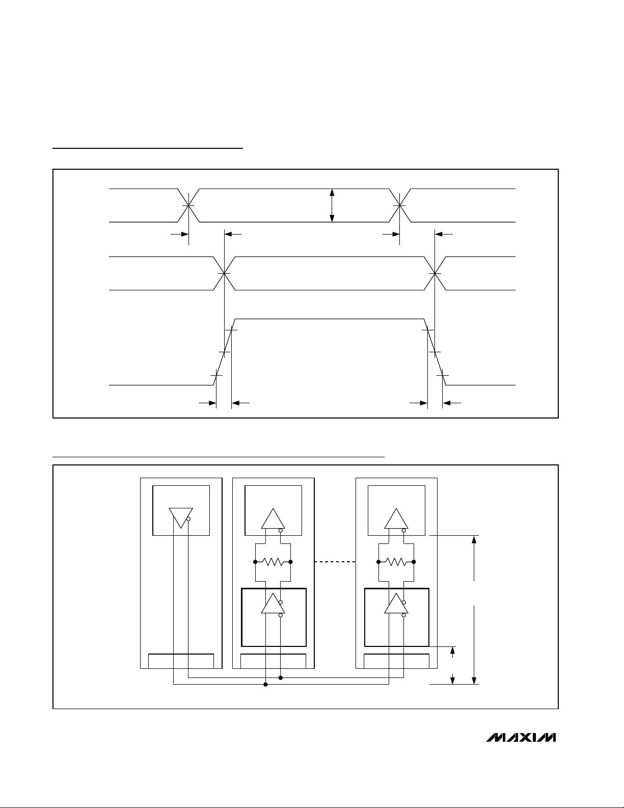
The MAX9155’s tiny size makes it especially suitable for
minimizing stub lengths in multidrop backplane applications. The SC70 package (half the size of a SOT23)
allows the MAX9155 to be placed close to the connector, thereby minimizing stub lengths and reflections on
the bus. The point-to-point connection between the
MAX9155 output and the destination IC, such as an
FPGA or ASIC, allows the destination IC to be located
at greater distances from the bus connector.
Ultra-low, 23ps
p-p
added deterministic jitter and
0.6ps
RMS
added random jitter ensure reliable communication in high-speed links that are highly sensitive to
timing errors, especially those incorporating clock-anddata recovery, PLLs, serializers, or deserializers. The
MAX9155’s switching performance guarantees a
200Mbps data rate, but minimizes radiated noise by
guaranteeing 0.5ns minimum output transition time.
The MAX9155 has fail-safe circuitry that sets the output
high for undriven open, short, or terminated inputs.
The MAX9155 operates from a single +3.3V supply and
consumes only 10mA over a -40°C to +85°C temperature range. Refer to the MAX9129 data sheet for a quad
bus LVDS driver, and to the MAX9156 data sheet for a
low-jitter, low-noise LVPECL-to-LVDS level translator in
an SC70 package.
Applications
Cellular Phone Base Stations
DSLAMs
Digital Cross-Connects
Add/Drop Muxes
Network Switches/Routers
Multidrop Buses
Cable Repeaters
Features
♦ Tiny SC70 Package
♦ Ultra-Low Jitter
23ps
p-p
Added Deterministic Jitter
(2
23
-1 PRBS)
0.6ps
RMS
Added Random Jitter
♦ 0.5ns (min) Transition Time Minimizes Radiated
Noise
♦ 200Mbps Guaranteed Data Rate
♦ Fail-Safe Circuit Sets Output High for Undriven
Inputs (Open, Terminated, or Shorted)
♦ Low 10mA Supply Current
♦ Low 6mA Supply Current in Fail-Safe
♦ Conforms to ANSI/EIA/TIA-644 LVDS Standard
♦ High-Impedance Inputs and Outputs in
Power-Down Mode
MAX9155
Low-Jitter, Low-Noise LVDS
Repeater in an SC70 Package
________________________________________________________________ Maxim Integrated Products 1
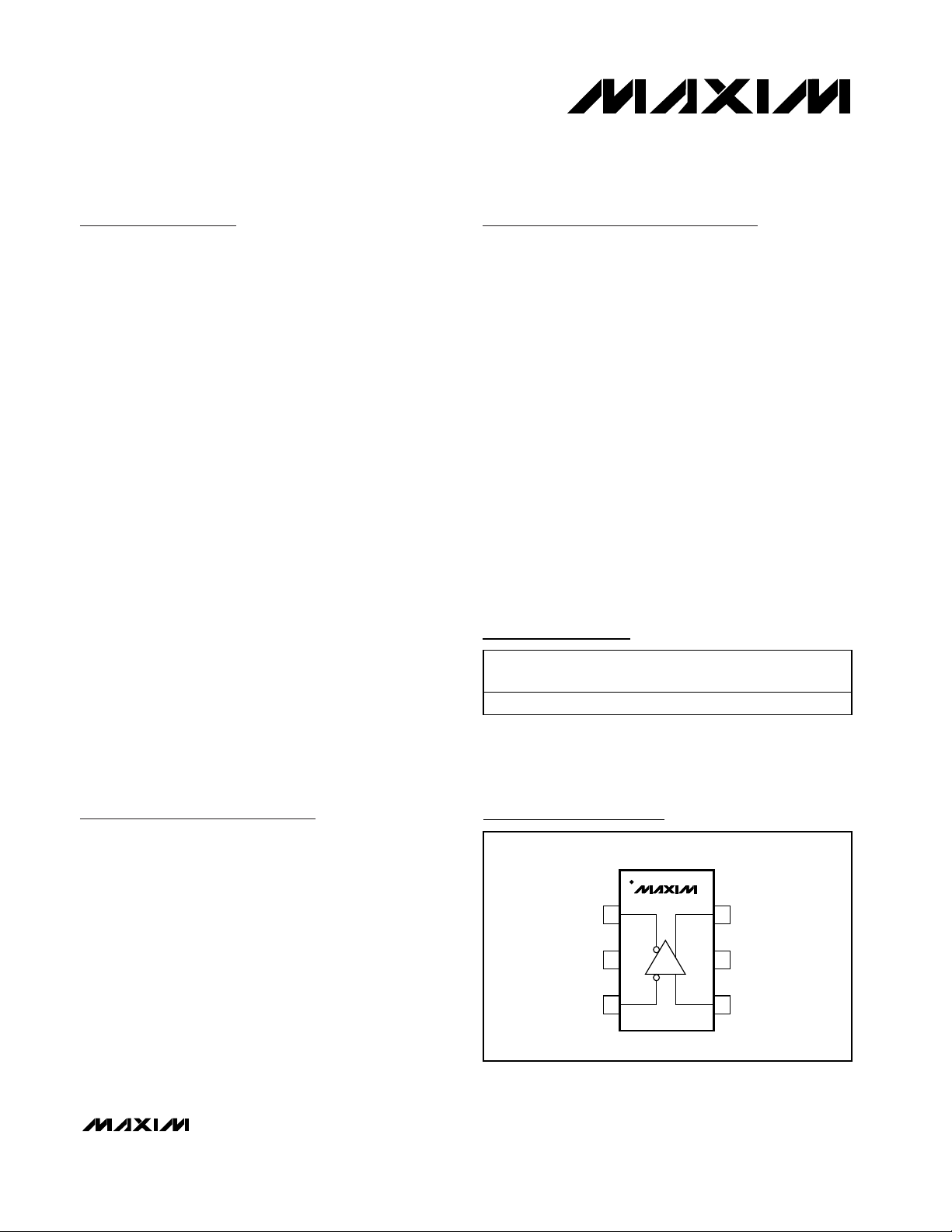
Pin Configuration
19-2213; Rev 0; 10/01
For pricing, delivery, and ordering information, please contact Maxim/Dallas Direct! at
1-888-629-4642, or visit Maxim’s website at www.maxim-ic.com.
Ordering Information
Typical Operating Circuit appears at end of data sheet.
PART TEMP. RANGE
MAX9155EXT-T -40°C to +85°C 6 SC70-6 ABC
PIN -
PA C K A G E
TOP
M ARK
TOP VIEW
1 6 OUT+
OUT-
GND
2
34
MAX9155
5V
CC
IN+IN-
SC70
Page 2
MAX9155
Low-Jitter, Low-Noise LVDS
Repeater in an SC70 Package
2 _______________________________________________________________________________________
ABSOLUTE MAXIMUM RATINGS
Stresses beyond those listed under “Absolute Maximum Ratings” may cause permanent damage to the device. These are stress ratings only, and functional
operation of the device at these or any other conditions beyond those indicated in the operational sections of the specifications is not implied. Exposure to
absolute maximum rating conditions for extended periods may affect device reliability.
VCCto GND...........................................................-0.3V to +4.0V
IN+, IN- to GND.....................................................-0.3V to +4.0V
OUT+, OUT- to GND .............................................-0.3V to +4.0V
Short-Circuit Duration (OUT+, OUT-) .........................Continuous
Continuous Power Dissipation (T
A
= +70°C)
6-Pin SC70 (derate 3.1mW/°C above +70°C)..............245mW
Storage Temperature Range .............................-65°C to +150°C
Junction Temperature......................................................+150°C
Operating Temperature Range ...........................-40°C to +85°C
ESD Protection
Human Body Model, IN+, IN-, OUT+, OUT- ....................±8kV
Lead Temperature (soldering, 10s) .................................+300°C
DC ELECTRICAL CHARACTERISTICS
(VCC= +3.0V to +3.6V, RL= 100Ω ±1%, |V
ID
|
= 0.05V to 1.2V, VCM= |VID/ 2|to 2.4V - |VID/ 2|, TA= -40°C to +85°C, unless otherwise
noted. Typical values are at V
CC
= +3.3V, TA= +25°C.) (Notes 1, 2)
LVDS INPUT
Differential Input High Threshold V
Differential Input Low Threshold V
Input Current I
Power-Off Input Current I
Input Resistor 1 R
Input Resistor 2 R
LVDS OUTPUT
Differential Output Voltage V
Change in VOD Between
Complementary Output States
Offset (Common-Mode) Voltage V
Change in VOS for
Complementary Output States
Output High Voltage V
Output Low Voltage V
Fail-Safe Differential Output
Voltage
Power-Off Output Leakage
Current
Differential Output Resistance RO
Output Short Current I
POWER SUPPLY
Supply Current I
Supply Current in Fail-Safe I
PARAMETER SYMBOL CONDITIONS MIN TYP MAX U N I T S
TH
TL
, I
IN+
IN-
, I
IN+
IN-
IN1
IN2
OD
∆V
OD
OS
∆V
OS
OH
OL
V
OD+
IO
OFF
DIFFVCC
SC
CC
CCF
0.05V ≤ |V
0.6V< |V
0.05V ≤ |V
0.6V < |V
VCC = +3.6V or 0, Figure 1 67 232 kΩ
VCC = +3.6V or 0, Figure 1 267 1174 kΩ
Figure 2 250 360 450 mV
Figure 2 0.008 25 mV
Figure 2 1.125 1.25 1.375 V
Figure 2 0.005 25 mV
IN+, IN- shorted, open, or parallel
terminated
VCC = 0
VID = +50mV, OUT+ = GND -5 -15
VID = -50mV, OUT- = GND -5 -15
Output loaded 10 15 mA
Output loaded, input undriven 6 8 mA
ID
≤ 1.2V, -20 -3.5 20
|
ID
ID
≤ 1.2V, V
|
ID
= +3.6V or 0 100 260 400 Ω
750mV
-50 -7 mV
≤ 0.6V -15 -2.5 15
|
≤0.6V, V
|
O U T+ = 3.6V , other outp ut op en -10 0.02 10
O U T- = 3.6V , other outp ut op en -10 0.02 10
= 0 -15 1.3 15
CC
= 0 -20 2.6 20
CC
1.44 1.6 V
0.9 1.08 V
+250 +360 +450 mV
µA
µA
µA
mA
Page 3
MAX9155
Low-Jitter, Low-Noise LVDS
Repeater in an SC70 Package
_______________________________________________________________________________________ 3
Note 1: All devices are 100% tested at TA= +25°C. Limits over temperature are guaranteed by design and characterization.
Note 2: Current into a pin is defined as positive. Current out of a pin is defined as negative. All voltages are referenced to ground
except V
TH
, VTL, VOD, and ∆VOD.
Note 3: Guaranteed by design and characterization.
Note 4: Signal generator output (unless otherwise noted): frequency = 100MHz, 50% duty cycle, R
O
= 50Ω, tR= 1.5ns, and tF=
1.5ns (0% to 100%).
Note 5: C
L
includes scope probe and test jig capacitance.
Note 6: Signal generator output for t
DJ
: VOD= 150mV, VOS= 1.2V, tDJincludes pulse (duty-cycle) skew.
Note 7: Signal generator output for t
RJ
: VOD= 150mV, VOS= 1.2V.
Note 8: t
SKPP1
is the magnitude difference of any differential propagation delays between devices operating over rated conditions
at the same supply voltage, input common-mode voltage, and ambient temperature.
Note 9: t
SKPP2
is the magnitude difference of any differential propagation delays between devices operating over rated conditions.
Note 10: Device meets V
OD
DC specification and AC specifications while operating at f
MAX
.
Note 11: Jitter added to the input signal.
AC ELECTRICAL CHARACTERISTICS
(VCC= +3.0V to +3.6V, RL= 100Ω ±1%, CL= 10pF, |V
ID
|
= 0.15V to 1.2V, VCM= |VID/ 2|to 2.4V - |VID/ 2|, TA= -40°C to +85°C,
unless otherwise noted. Typical values are at V
CC
= +3.3V, TA= +25°C.) (Notes 3, 4, 5) (Figures 3, 4)
p-p
Differential Propagation Delay High to
Low
Differential Propagation Delay Low to
High
Added Deterministic Jitter (Notes 6, 11) t
Added Random Jitter (Notes 7, 11) t
Differential Part-to-Part Skew (Note 8) t
Differential Part-to-Part Skew (Note 9) t
Switching Supply Current I
Rise Time t
Fall Time t
Input Frequency (Note 10) f
PARAMETER SYMBOL CONDITIONS MIN TYP MAX U N I T S
t
PHLD
t
PLHD
DJ
RJ
SKPP1
SKPP2
CCSW
TLH
THL
MAX
1.3 2.0 2.8 ns
1.3 2.0 2.8 ns
200Mbps 223-1 PRBS data pattern 23 100 ps
fIN = 100MHz 0.6 2.9 ps
0.17 0.6 ns
1.5 ns
11.3 18 mA
0.5 0.66 1.0 ns
0.5 0.64 1.0 ns
100 MHz
RMS
Page 4
MAX9155
Low-Jitter, Low-Noise LVDS
Repeater in an SC70 Package
4 _______________________________________________________________________________________
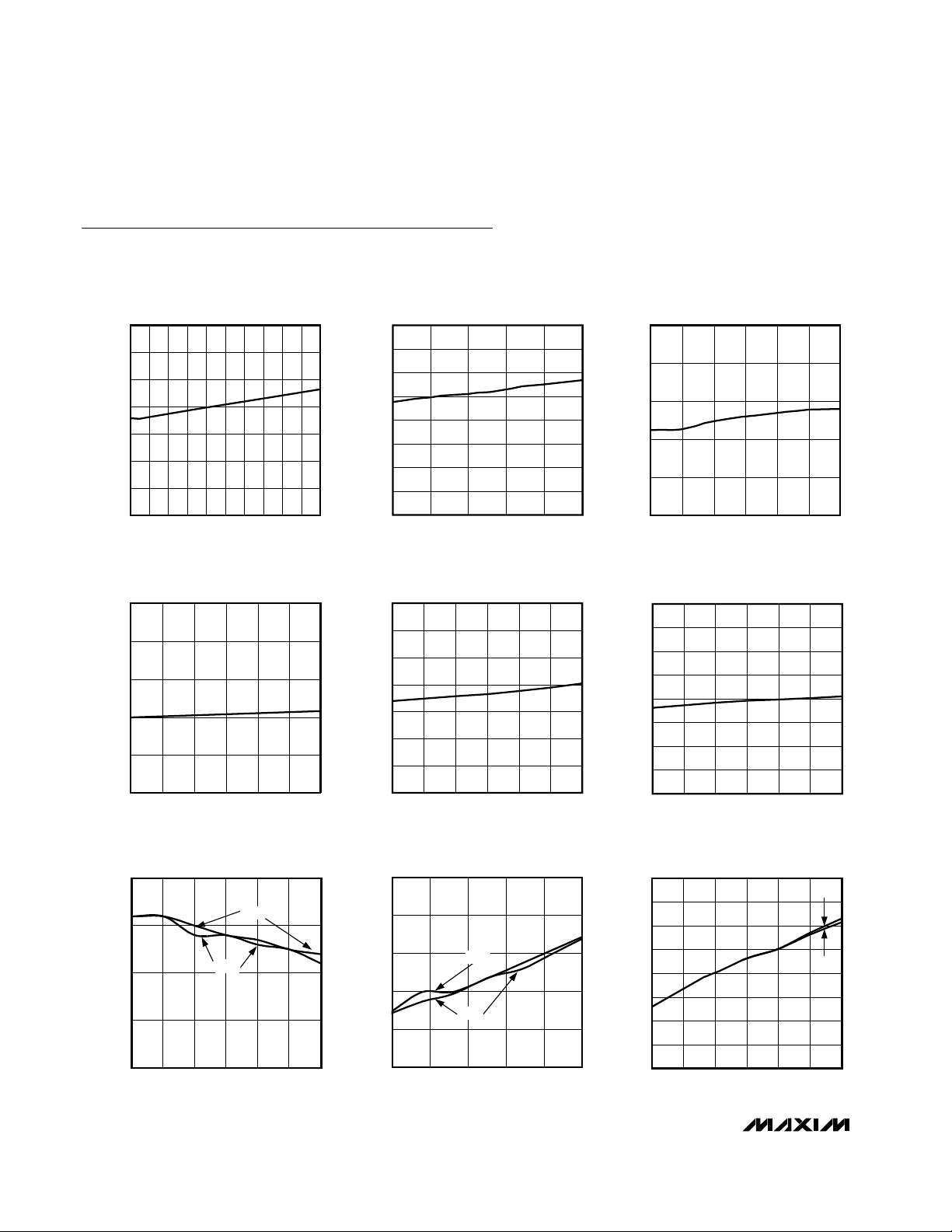
Typical Operating Characteristics
(VCC= +3.3V, RL= 100Ω ±1%, CL= 10pF, |V
ID
|
= 0.2V, VCM= 1.2V, TA= +25°C, unless otherwise noted. Signal generator output:
frequency = 100MHz, 50% duty cycle, R
O
= 50Ω, tR= 1.5ns, and tF= 1.5ns (0% to 100%), unless otherwise noted.)
SUPPLY CURRENT
21
18
15
12
9
SUPPLY CURRENT (mA)
6
3
0
VS. INPUT FREQUENCY
0 10050 150 20025 12575 175 225 250
INPUT FREQUENCY (MHz)
SWITCHING SUPPLY CURRENT
12.00
11.75
MAX9155 toc01
11.50
11.25
11.00
10.75
SUPPLY CURRENT (mA)
10.50
10.25
10.00
-40 -15 10 35 60 85
VS. TEMPERATURE
TEMPERATURE (°C)
OUTPUT SHORT-CIRCUIT CURRENT
5.10
MAX9155 toc02
5.09
5.08
5.07
5.06
OUTPUT SHORT-CIRCUIT CURRENT (mA)
5.05
3.0 3.23.1 3.3 3.4 3.5 3.6
VS. SUPPLY VOLTAGE
SUPPLY VOLTAGE (V)
MAX9155 toc03
FAIL-SAFE SUPPLY CURRENT
6.5
6.3
6.1
5.9
SUPPLY CURRENT (mA)
5.7
5.5
3.0 3.23.1 3.3 3.4 3.5 3.6
VS. SUPPLY VOLTAGE
SUPPLY VOLTAGE (V)
DIFFERENTIAL PROPAGATION DELAY
2.1
2.0
1.9
1.8
DIFFERENTIAL PROPAGATION DELAY (ns)
1.7
3.0 3.33.1 3.2 3.4 3.5 3.6
VS. SUPPLY VOLTAGE
t
PHLD
t
PLHD
SUPPLY VOLTAGE (V)
OUTPUT LOW VOLTAGE
1.12
1.11
MAX9155 toc04
1.10
1.09
1.08
1.07
OUTPUT LOW VOLTAGE (V)
1.06
1.05
3.0 3.2 3.33.1 3.4 3.5 3.6
VS. SUPPLY VOLTAGE
DIFFERENTIAL PROPAGATION DELAY
2.5
MAX9155 toc07
2.3
2.1
1.9
1.7
DIFFERENTIAL PROPAGATION DELAY (ns)
1.5
-40 10-15 35 60 85
SUPPLY VOLTAGE (V)
VS. TEMPERATURE
t
PHLD
t
PLHD
TEMPERATURE (°C)
1.550
1.525
MAX9155 toc05
1.500
1.475
1.450
1.425
OUTPUT HIGH VOLTAGE (V)
1.400
1.375
1.350
3.0 3.23.1 3.3 3.4 3.5 3.6
750
725
MAX9155 toc08
700
675
650
625
TRANSITION TIME (ps)
600
575
550
3.0 3.23.1 3.3 3.4 3.5 3.6
OUTPUT HIGH VOLTAGE
VS. SUPPLY VOLTAGE
SUPPLY VOLTAGE (V)
TRANSITION TIME
VS. SUPPLY VOLTAGE
SUPPLY VOLTAGE (V)
MAX9155 toc06
t
THL
MAX9155 toc09
t
TLH
Page 5

Detailed Description
The LVDS interface standard is a signaling method
intended for point-to-point communication over a controlled-impedance medium, as defined by the ANSI/
TIA/EIA-644 and IEEE 1596.3 standards. The LVDS
standard uses a lower voltage swing than other common communication standards, achieving higher data
rates with reduced power consumption while reducing
EMI emissions and system susceptibility to noise.
The MAX9155 is a 200Mbps LVDS repeater intended
for high-speed, point-to-point, low-power applications.
The MAX9155 accepts an LVDS input and reproduces
an LVDS signal at the output. This device is capable of
detecting differential signals as low as 50mV and as
high as 1.2V within a 0 to 2.4V input voltage range. The
LVDS standard specifies an input voltage range of 0 to
2.4V referenced to ground.
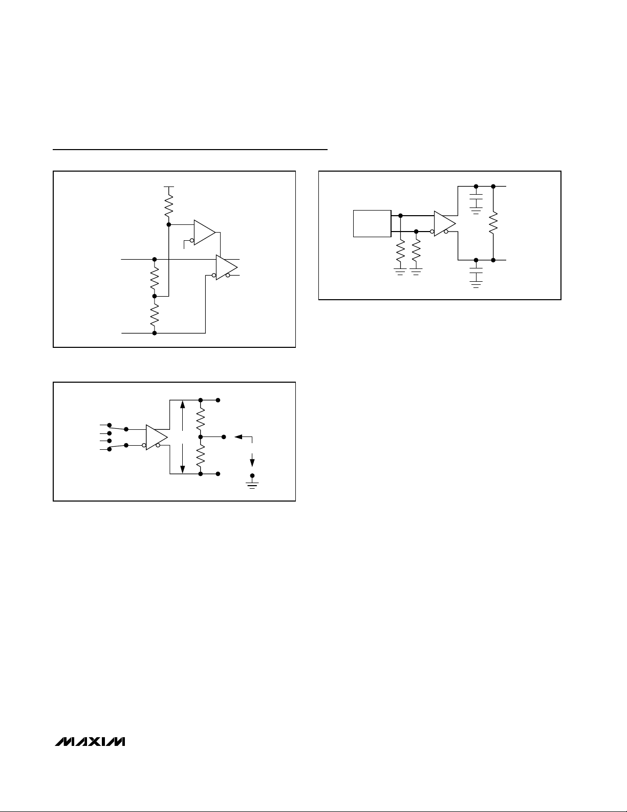
Fail-Safe
Fail-safe is a feature that puts the output in a known
logic state (differential high) under certain fault conditions. The MAX9155 outputs are differential high when
the inputs are undriven and open, terminated, or shorted
(Table 1).
MAX9155
Low-Jitter, Low-Noise LVDS
Repeater in an SC70 Package
_______________________________________________________________________________________ 5
Typical Operating Characteristics (continued)
(VCC= +3.3V, RL= 100Ω ±1%, CL= 10pF, |V
ID
|
= 0.2V, VCM= 1.2V, TA= +25°C, unless otherwise noted. Signal generator output:
frequency = 100MHz, 50% duty cycle, R
O
= 50Ω, tR= 1.5ns, and tF= 1.5ns (0% to 100%), unless otherwise noted.)
Pin Description
Note: VID= (IN+ - IN-), VOD= (OUT+ - OUT-)
High = 450mV ≥ V
OD
≥ 250mV
Low = -250mV ≥ V
OD
≥ -450mV
Table 1. Function Table for LVDS Fail-Safe
Input (Figure 2)
800
750
700
650
600
550
TRANSITION TIME (ps)
500
450
400
-40 -15 10 35 60 85
PIN NAME FUNCTION
1 OUT- Inverting LVDS Output
2 GND Ground
3 IN- Inverting LVDS Input
4 IN+ Noninverting LVDS Input
5V
6 OUT+ Noninverting LVDS Output
CC
Power Supply. Bypass VCC to GND
with 0.01µF ceramic capacitor.
TRANSITION TIME
VS. TEMPERATURE
t
, t
TLH
TEMPERATURE (°C)
THL
Undriven open, short, or terminated High
INPUT, V
50mV > VID > -50mV Indeterminate
ID
> 50mV High
< -50mV Low
OUTPUT, V
OD
DIFFERENTIAL OUTPUT VOLTAGE
600
MAX9155 toc10
500
400
300
200
100
DIFFERENTIAL OUTPUT VOLTAGE (mV)
0
25 150
VS. LOAD RESISTOR
MAX9155 toc11
7550 100 125
LOAD RESISTOR (Ω)
Page 6

MAX9155
Applications Information
Supply Bypassing
Bypass VCCwith a high-frequency surface-mount
ceramic 0.01µF capacitor as close to the device as
possible.
Differential Traces
Input and output trace characteristics affect the performance of the MAX9155. Use controlled-impedance differential traces. Ensure that noise couples as common
mode by running the traces within a differential pair
close together.
Maintain the distance within a differential pair to avoid
discontinuities in differential impedance. Avoid 90°
turns and minimize the number of vias to further prevent
impedance discontinuities.
Cables and Connectors
The LVDS standards define signal levels for interconnect with a differential characteristic impedance and
termination of 100Ω. Interconnects with a characteristic
impedance and termination of 90Ω to 132Ω impedance
are allowed, but produce different signal levels (see
Termination).
Use cables and connectors that have matched differential impedance to minimize impedance discontinuities.
Avoid the use of unbalanced cables, such as ribbon or
coaxial cable. Balanced cables, such as twisted pair,
offer superior signal quality and tend to generate less
EMI due to canceling effects. Balanced cables tend to
pick up noise as common mode, which is rejected by
the LVDS receiver.
Termination
For point-to-point links, the termination resistor should
be located at the LVDS receiver input and match the
differential characteristic impedance of the transmission line.
For a multidrop bus driven at one end, terminate at the
other end of the bus with a resistor that matches the
loaded differential characteristic impedance of the bus.
For a multidrop bus driven from a point other than the
end, terminate each end of the bus with a resistor that
matches the loaded differential characteristic impedance of the bus. When terminating at both ends, or for a
large number of drops, a bus LVDS (BLVDS) driver is
needed to drive the bus to LVDS signal levels. The
MAX9155 is not intended to drive double-terminated
multidrop buses to LVDS levels.
The differential output voltage level depends upon the
differential characteristic impedance of the interconnect
and the value of the termination resistance. The
MAX9155 is guaranteed to produce LVDS output levels
into 100Ω. With the typical 3.6mA output current, the
MAX9155 produces an output voltage of 360mV when
driving a 100Ω transmission line terminated with a
100Ω termination resistor (3.6mA x 100Ω = 360mV). For
typical output levels with different loads, see the
Differential Output Voltage vs. Load Resistor typical
operating curve.
Chip Information
TRANSISTOR COUNT: 401
PROCESS: CMOS
Low-Jitter, Low-Noise LVDS
Repeater in an SC70 Package
6 _______________________________________________________________________________________
Page 7
MAX9155
Low-Jitter, Low-Noise LVDS
Repeater in an SC70 Package
_______________________________________________________________________________________ 7
Figure 1. LVDS Fail-Safe Input
Figure 2. DC Load Test Circuit
Figure 3. Transition Time and Propagation Delay Test Circuit
Test Circuit and Timing Diagrams
R
IN2
R
/2
IN1
R
/2
IN1
IN-
1.25V
1.20V
1.25V
1.20V
IN+
IN-
V
CC
VCC - 0.3V
C
L
IN+
IN-
50Ω50Ω
C
L
OUT+IN+
OUT-
PULSE
GENERATOR
OUT+
/2
R
L
V
OD
R
/2
L
V
OS
OUT+
R
L
OUT-
OUT-
Page 8
MAX9155
Low-Jitter, Low-Noise LVDS
Repeater in an SC70 Package
8 _______________________________________________________________________________________
Test Circuit and Timing Diagrams (continued)
Figure 4. Transition Time and Propagation Delay Timing Diagram
Typical Operating Circuit
V
= ((IN+) + (IN-))/2
IN-
IN+
OUT-
OUT+
O (DIFFERENTIAL)
t
PLHD
O (DIFFERENTIAL)
CM
VID
80% 80%
O (DIFFERENTIAL)
t
PHLD
O (DIFFERENTIAL)
O (DIFFERENTIAL)
V
DIFF
20% 20%
t
TLH
1/4
MAX9129
1/4
MAX9121
100Ω 100Ω
MAX9155 MAX9155
V
= (OUT+) - (OUT-)
DIFF
O (DIFFERENTIAL)
t
THL
1/4
MAX9121
STUB
WITHOUT
REPEATER
STUB WITH
REPEATER
REPEATERS REDUCE ASIC OR FPGA STUB LENGTH ON A MULTIDROP BUS.
Page 9

MAX9155
Low-Jitter, Low-Noise LVDS
Repeater in an SC70 Package
Maxim cannot assume responsibility for use of any circuitry other than circuitry entirely embodied in a Maxim product. No circuit patent licenses are
implied. Maxim reserves the right to change the circuitry and specifications without notice at any time.
Maxim Integrated Products, 120 San Gabriel Drive, Sunnyvale, CA 94086 408-737-7600 _____________________ 9
© 2001 Maxim Integrated Products Printed USA is a registered trademark of Maxim Integrated Products.
Package Information
SC70, 6L.EPS
 Loading...