

Page 1
General Description
The MAX9152 2 x 2 crosspoint switch is designed for
applications requiring high speed, low power, and lownoise signal distribution. This device includes two
LVDS/LVPECL inputs, two LVDS outputs, and two logic
inputs that set the internal connections between differential inputs and outputs.
The MAX9152 can be programmed to connect any
input to either or both outputs, allowing it to be used in
the following configurations: 2 ✕2 crosspoint switch, 2:1
mux, 1:2 demux, 1:2 splitter, or dual repeater. This flexibility makes the MAX9152 ideal for protection switching
in fault-tolerant systems, loopback switching for diagnostics, fanout buffering for clock/data distribution, and
signal regeneration for communication over extended
distances.
Ultra-low 120ps
PK-PK
(max) PRBS jitter ensures reliable
communications in high-speed links that are highly sensitive to timing error, especially those incorporating
clock-and-data recovery, or serializers and deserializers. The high-speed switching performance guarantees
an 800Mbps data rate and less than 50ps (max) skew
between channels.
LVDS inputs and outputs are compatible with the
TIA/EIA-644 LVDS standard. The LVDS inputs are
designed to also accept LVPECL signals directly, and
PECL signals with an attenuation network. The LVDS
outputs are designed to drive 75Ω or 100Ω loads, and
feature a selectable differential output resistance to
minimize reflections.
The MAX9152 is available in 16-pin TSSOP and SO
packages, and consumes only 109mW while operating
from a single +3.3V supply over the -40°C to +85°C
temperature range.
Applications
Cell Phone Base Stations
Add/Drop Muxes
Digital Crossconnects
DSLAMs
Network Switches/Routers
Protection Switching
Loopback Diagnostics
Clock/Data Distribution
Cable Repeaters
Features
♦ Pin-Programmable Configuration
2 x 2 Crosspoint Switch
2:1 Mux
1:2 Demux
1:2 Splitter
Dual Repeater
♦ Ultra-Low 120ps
PK-PK
(max) Jitter with 800Mbps,
PRBS = 2
23
-1 Data Pattern
♦ Low 50ps (max) Channel-to-Channel Skew
♦ 109mW Power Dissipation
♦ Compatible with ANSI TIA/EIA-644 LVDS Standard
♦ Inputs Accept LVDS/LVPECL Signals
♦ LVDS Output Rated for 75Ω and 100Ω Loads
♦ Pin-Programmable Differential Output Resistance
♦ Pin-Compatible Upgrade to DS90CP22
(SO Package)
♦ Available in 16-Pin TSSOP Package
(Half the Size of SO)
MAX9152
800Mbps LVDS/LVPECL-to-LVDS 2 x 2
Crosspoint Switch
________________________________________________________________ Maxim Integrated Products 1
19-2003; Rev 0; 4/01
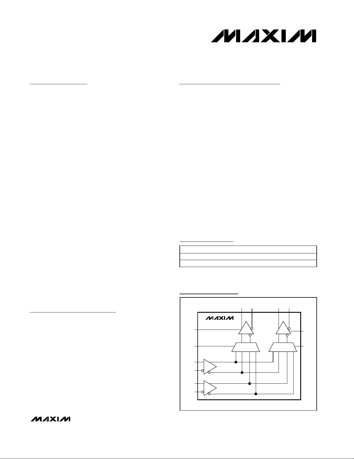
EN0
SEL0
IN0+
IN0-
IN1+
IN1-
MAX9152
01 01
EN1
SEL1
OUT1-OUT1+OUT0-OUT0+
Functional Diagram
Ordering Information
Pin Configuration appears at end of data sheet.
For pricing, delivery, and ordering information, please contact Maxim/Dallas Direct! at
1-888-629-4642, or visit Maxim’s website at www.maxim-ic.com.
PART TEMP. RANGE PIN-PACKAGE
MAX9152ESE -40°C to +85°C 16 SO
MAX9152EUE -40°C to +85°C 16 TSSOP
Page 2
MAX9152
800Mbps LVDS/LVPECL-to-LVDS 2 x 2
Crosspoint Switch
2 _______________________________________________________________________________________
ABSOLUTE MAXIMUM RATINGS
DC ELECTRICAL CHARACTERISTICS
(VCC= +3.0V to +3.6V, NC/RSEL = open for RL= 75Ω ±1%, NC/RSEL = high for RL= 100Ω ±1%, differential input voltage |VID| =
0.1V to V
CC
, input voltage (V
IN+
, V
IN-
) = 0 to VCC, EN_ = high, SEL0 = low, SEL1 = high, and TA= -40°C to +85°C. Typical values at
V
CC
= +3.3V, |VID| = 0.2V, input common-mode voltage VCM= 1.2V, TA= +25°C, unless otherwise noted.) (Note 1)
Stresses beyond those listed under “Absolute Maximum Ratings” may cause permanent damage to the device. These are stress ratings only, and functional
operation of the device at these or any other conditions beyond those indicated in the operational sections of the specifications is not implied. Exposure to
absolute maximum rating conditions for extended periods may affect device reliability.
VCCto GND...........................................................-0.3V to +4.0V
IN_+, IN_-, OUT_+, OUT_- to GND .......................-0.3V to +4.0V
EN_, SEL_, NC/RSEL to GND.....................-0.3V to (VCC+ 0.3V)
Short-Circuit Duration (OUT_+, OUT_-) .....................Continuous
Continuous Power Dissipation (T
A
= +70°C)
16-Pin SO (derate 8.7mW/°C above +70°C)................696mW
16-Pin TSSOP (derate 9.4mW/°C above +70°C) .........755mW
Storage Temperature Range .............................-65°C to +150°C
Junction Temperature......................................................+150°C
Operating Temperature Range ...........................-40°C to +85°C
Lead Temperature (soldering, 10s) .................................+300°C
ESD Protection
Human Body Model, IN_+, IN_-, OUT_+, OUT_-........... ±7kV
,
LVCMOS/LVTTL INPUTS (EN_, SEL_)
Input High Voltage V
Input Low Voltage V
Input High Current I
Input Low Current I
NC/RSEL INPUT
Input High Voltage V
Input Low Voltage V
Input High Current I
Input Low Current I
DIFFERENTIAL INPUTS (IN_+, IN_-)
Differential Input High Threshold V
Differential Input Low Threshold V
Input Current I
LVDS OUTPUTS (OUT_+, OUT_-)
Differential Output Impedance
(Note 2)
Differential Output Voltage V
Change in Magnitude of V
Between Complementary Output
States
Offset Common-Mode Voltage V
Change in Magnitude of V
Between Complementary Output
States
PARAMETER SYMBOL CONDITIONS MIN TYP MAX UNITS
OD
OS
IH
IL
VIN = VCC or 2.0V 0 20 µA
VIN = 0 or 0.8V -10 10 µA
VIN = VCC or 2.0V 0 20 µA
VIN = 0 or 0.8V -10 10 µA
V
= VCC or 0, V
IN+
I
IN-
V
= 3. 6 V o r 0 , V
I N +
= 0
V
C C
NC/RSEL = low or open 60 90 118
NC/RSEL = high 85 122 155
RL = 75Ω, NC/RSEL = open, Figure 1
RL = 100Ω, NC/RSEL = high, Figure 1
IN+
R
IH
IL
IH
IL
IH
IL
TH
TL
DIFF
OD
RL = 75Ω, NC/RSEL = open, Figure 1
∆V
OD
RL = 100Ω, NC/RSEL = high, Figure 1
OS
RL = 75Ω, NC/RSEL = open, Figure 1
RL = 100Ω, NC/RSEL = high, Figure 1
RL = 75Ω, NC/RSEL = open, Figure 1
∆V
OS
RL = 100Ω, NC/RSEL = high, Figure 1
2.0 V
CC
GND 0.8 V
2.0 V
CC
GND 0.8 V
100 mV
-100 mV
= V
IN-
I N -
or 0 -1 1
CC
= 3 . 6 V or 0 ,
-1 1
280 382 470 mV
25 mV
1.150 1.430 V
25 mV
V
V
µA
Ω
Page 3
MAX9152
800Mbps LVDS/LVPECL-to-LVDS 2 x 2
Crosspoint Switch
_______________________________________________________________________________________ 3
DC ELECTRICAL CHARACTERISTICS (continued)
(VCC= +3.0V to +3.6V, NC/RSEL = open for RL= 75Ω ±1%, NC/RSEL = high for RL= 100Ω ±1%, differential input voltage |VID| =
0.1V to V
CC
, input voltage (V
IN+
, V
IN-
) = 0 to VCC, EN_ = high, SEL0 = low, SEL1 = high, and TA= -40°C to +85°C. Typical values at
V
CC
= +3.3V, |VID| = 0.2V, input common-mode voltage VCM= 1.2V, TA= +25°C, unless otherwise noted.) (Note 1)
AC ELECTRICAL CHARACTERISTICS
(VCC= +3.0V to +3.6V, NC/RSEL = open for RL= 75Ω ±1%, NC/RSEL = high for RL= 100Ω ±1%, CL= 5pF, differential input voltage
|V
ID
| = 0.15V to VCC, EN_ = high, SEL0 = low, SEL1 = high, differential input transition time = 0.6ns (20% to 80%), input voltage
(V
IN+
, V
IN-
) = 0 to VCC, LVCMOS/LVTTL inputs = 0 to 3V with 2ns (10% to 90%) transition times, TA= -40°C to +85°C. Typical values
at V
CC
= +3.3V, |VID| = 0.2V, VCM= 1.2V, TA= +25°C, unless otherwise noted.) (Notes 3, 4)
Output Short-Circuit Current I
Both Output Short-Circuit Current I
Output High-Z Current I
Power-Off Output Current I
SUPPLY CURRENT
Supply Current I
High-Z Supply Current I
PARAMETER SYMBOL CONDITIONS MIN TYP MAX UNITS
OS
VID = +100mV, V
open
VID = -100mV, V
= 0, other output
OUT_+
= 0,
OUT_-
-12 -20 mA
other output open
OSB
, I
OZ+
OZ-
OFF+, IOFF-
CC
CCZ
VID = +100mV, V
VID = -100mV, V
Disabled, V
V
OUT_-
V
CC
V
OUT_-
= VCC or 0
= 0, V
= 3.6V or 0
OUT_+
OUT_+
RL = 75Ω, CL = 5pF, enabled, quiescent,
Figure 5
RL = 100Ω, CL = 5pF, enabled, quiescent,
Figure 5
RL = 75Ω, CL = 5pF, enabled, switching
at 400MHz (800Mbps), Figure 5 (Note 2)
RL = 100Ω, CL = 5pF, enabled, switching
at 400MHz (800Mbps), Figure 5 (Note 2)
Disabled 15 25 mA
= 0, V
OUT_+
= 0, V
OUT_+
= VCC or 0,
= 3.6V or 0,
OUT_-
OUT_-
= 0
= 0
-12 -20 mA
-1 1 µA
-1 1 µA
38 55
33 50
58 70
52 65
mA
Input to SEL Setup Time (Note 5) t
Input to SEL Hold Time (Note 5) t
SEL to Switched Output t
Disable Time High to Z t
Disable Time Low to Z t
Enable Time Z to High t
Enable Time Z to Low t
Propagation Low-to-High Delay t
Propagation High-to-Low Delay t
PARAMETER SYMBOL CONDITIONS MIN TYP MAX UNITS
SET
HOLD
SWITCH
PHZ
PLZ
PZH
PZL
PLHD
PHLD
Figures 2, 3 0.4 ns
Figures 2, 3 0.6 ns
Figures 2, 3 1.8 2.5 3.5 ns
Figure 4 3.8 ns
Figure 4 3.8 ns
Figure 4 3.2 ns
Figure 4 3.2 ns
Figures 5, 6 1.7 2.3 3.4
V
= +3.3V, TA = +25°C; Figures 5, 6 2.0 2.3 2.9
CC
Figures 5, 6 1.7 2.3 3.4
VCC = +3.3V, TA = +25°C; Figures 5, 6 2.0 2.3 2.9
ns
ns
Page 4
DIFFERENTIAL OUTPUT EYE PATTERN
IN 1:2 SPLITTER MODE AT 800Mbps
CONDITIONS: 3.3V, PRBS = 223 -1 DATA PATTERN,
|V
ID
| = 200mV, VCM = +1.2V
HORIZONTAL SCALE = 200ps/div
VERTICAL SCALE = 100mV/div
MAX9152 toc01
150
250
350
450
550
650
50 10075 125 150 175 200
DIFFERENTIAL
OUTPUT VOLTAGE vs. LOAD
MAX9152 toc02
LOAD RESISTOR (Ω)
DIFFERENTIAL OUTPUT VOLTAGE (mV)
NC/RSEL = LOW OR OPEN
NC/RSEL = HIGH
30
32
36
34
38
40
100 300200 400 500 600 700 800
SUPPLY CURRENT vs. DATA RATE
MAX9152 toc03
DATA RATE (Mbps)
SUPPLY CURRENT (mA)
Typical Operating Characteristics
(VCC= +3.3V, RL= 100Ω, NC/RSEL = high, CL= 5pF, input transition time = 600ps (20% to 80%), VID= 200mV, PRBS = 223- 1 data
pattern, VCM= +1.2V, TA= +25°C, unless otherwise noted.)
MAX9152
800Mbps LVDS/LVPECL-to-LVDS 2 x 2
Crosspoint Switch
4 _______________________________________________________________________________________
AC ELECTRICAL CHARACTERISTICS (continued)
(VCC= +3.0V to +3.6V, NC/RSEL = open for RL= 75Ω ±1%, NC/RSEL = high for RL= 100Ω ±1%, CL= 5pF, differential input voltage
|V
ID
| = 0.15V to VCC, EN_ = high, SEL0 = low, SEL1 = high, differential input transition time = 0.6ns (20% to 80%), input voltage
(V
IN+
, V
IN-
) = 0 to VCC, LVCMOS/LVTTL inputs = 0 to 3V with 2ns (10% to 90%) transition times, TA= -40°C to +85°C. Typical values
at V
CC
= +3.3V, |VID| = 0.2V, VCM= 1.2V, TA= +25°C, unless otherwise noted.) (Notes 3, 4)
Note 1: Current into a pin is defined as positive. Current out of a pin is defined as negative. All voltages are referenced to ground
except V
TH
, VTL, VID, VOD, and ∆VOD.
Note 2: Guaranteed by design and characterization, not production tested.
Note 3: AC parameters are guaranteed by design and characterization.
Note 4: C
L
includes scope probe and test jig capacitance.
Note 5: t
SET
and t
HOLD
time specify that data must be in a stable state before and after the SEL transition.
Note 6: t
SKEW
is the magnitude difference of differential propagation delay over rated conditions; t
SKEW
= |t
PHLD
- t
PLHD
|.
Note 7: Specification includes test equipment jitter.
Pulse Skew |t
Output Channel-to-Channel Skew t
Output Low-to-High Transition
Time (20% to 80%)
Output High-to-Low Transition
Time (20% to 80%)
LVDS Data Path Peak-to-Peak
Jitter (Note 7)
PARAMETER SYMBOL CONDITIONS MIN TYP MAX UNITS
-t
PLHD
| (Note 6) t
PHLD
SKEW
CCS
t
LHT
t
HLT
Figures 5, 6 25 90 ps
Figures 5, 7 20 50 ps
Figures 5, 6 160 270 480 ps
Figures 5, 6 160 270 480 ps
VID = 200mV, VCM = 1.2V, 50% duty
cycle, 800Mbps, input transition time =
t
JIT
600ps (20% to 80%)
V
= 200mV, VCM = 1.2V, PRBS = 2
ID
23
- 1
data pattern, 800Mbps, input transition
10 30
65 120
time = 600ps (20% to 80%)
ps
Page 5

MAX9152
800Mbps LVDS/LVPECL-to-LVDS 2 x 2
Crosspoint Switch
_______________________________________________________________________________________ 5
Typical Operating Characteristics (continued)
(VCC= +3.3V, RL= 100Ω, NC/RSEL = high, CL= 5pF, input transition time = 600ps (20% to 80%), VID= 200mV, PRBS = 223- 1 data
pattern, V
CM
= +1.2V, TA= +25°C, unless otherwise noted.)
80
70
60
50
PEAK-TO-PEAK JITTER (ps)
40
30
PEAK-TO-PEAK OUTPUT JITTER
= VID/2 vs. DATA RATE
AT V
CM
MAX9152 toc04
VID = 0.2V
VID = 0.8V
VID = 0.4V
100 300200 400 500 600 700 800
DATA RATE (Mbps)
PEAK-TO-PEAK OUTPUT JITTER
= +0.4V vs. DATA RATE
AT V
80
CM
PEAK-TO-PEAK OUTPUT JITTER
= +1.2V vs. DATA RATE
AT V
80
70
60
50
PEAK-TO-PEAK JITTER (ps)
40
30
CM
VID = 0.2V
VID = 0.8V
VID = 0.4V
100 300200 400 500 600 700 800
DATA RATE (Mbps)
AT V
90
80
MAX9152 toc05
70
60
50
PEAK-TO-PEAK JITTER (ps)
40
30
100 400 500200 300 600 700 800
PEAK-TO-PEAK OUTPUT JITTER
= +1.6V vs. DATA RATE
AT V
80
CM
PEAK-TO-PEAK OUTPUT JITTER
= +3.3V - (VID/2) vs. DATA RATE
CM
VID = 0.2V
VID = 0.8V
VID = 0.4V
DATA RATE (Mbps)
MAX9152 toc06
70
60
50
PEAK-TO-PEAK JITTER (ps)
40
VID = 0.8V
30
100 300200 400 500 600 700 800
VID = 0.4V
VID = 0.2V
DATA RATE (Mbps)
MAX9152 toc07
70
60
50
PEAK-TO-PEAK JITTER (ps)
40
30
100 300200 400 500 600 700 800
VID = 0.8V
VID = 0.4V
DATA RATE (Mbps)
VID = 0.2V
MAX9152 toc08
Page 6

Detailed Description
The LVDS interface standard is a signaling method
intended for point-to-point communication over a controlled impedance medium as defined by the ANSI
TIA/EIA-644 and IEEE 1596.3 standards. LVDS uses a
lower voltage swing than other common communication
standards, achieving higher data rates with reduced
power consumption while reducing EMI emissions and
system susceptibility to noise.
The MAX9152 is an 800Mbps 2 x 2 crosspoint switch
designed for high-speed, low-power point-to-point and
multidrop interfaces. The device accepts LVDS or differential LVPECL signals and routes them to outputs
depending on the selected mode of operation.
A differential input with a magnitude of 0.1V to VCCwith
single-ended voltage levels at or within the MAX9152's
VCCand ground switches the output. A differential input
with a magnitude of at least 0.15V with single-ended voltage levels at or within the MAX9152's VCCand ground is
required to meet the AC specifications.
In the 1:2 splitter mode, the outputs repeat the selected
input. This is useful for distributing a signal or creating
a copy for use in protection switching. In the repeater
mode, the device operates as a two-channel buffer.
Repeating restores signal amplitude, allowing isolation
of media segments or longer media drive. The device is
a crosspoint switch where any input can be connected
to any output or outputs. In 2:1 mux mode, primary and
backup signals can be selected to provide a protection-switched, fault-tolerant application.
MAX9152
800Mbps LVDS/LVPECL-to-LVDS 2 x 2
Crosspoint Switch
6 _______________________________________________________________________________________
Pin Description
Figure 1. Test Circuit for VODand V
OS
PIN NAME FUNCTION
1, 2 SEL1, SEL0 LVCMOS/LVTTL Logic Inputs. Allow the switch to be configured as a mux, repeater, or splitter.
3, 4 IN0+, IN0- LVDS/LVPECL Differential Input 0
5VCCPower-Supply Input. Bypass VCC to GND with 0.1µF and 0.001µF ceramic capacitors.
6, 7 IN1+, IN1- LVDS/LVPECL Differential Input 1
8 NC/RSEL
9 NC No Connect
10, 11
12 GND Ground
13, 14
15, 16 EN1, EN0
OUT1-,
OUT1+
OUT0-,
OUT0+
Logic Input. Selects differential output resistance. Set NC/RSEL to open or low when R
set to high when R
LVDS Differential Output 1
LVDS Differential Output 0
LVCMOS/LVTTL Logic Inputs. Enables or disables the outputs. Setting EN0 or EN1 high
enables the corresponding output, OUT0 or OUT1. Setting EN0 or EN1 low puts the
corresponding output into high impedance (differential output resistance is also high
impedance).
= 100Ω.
L
= 75Ω,
L
1/2 MAX9152
IN_+
IN_-
OUT_+
R
R
/2
L
/2
L
VID = (V
IN_+
) - (V
IN_-
ENABLED
)
OUT_-
∆V
= VOD - VOD*
OD
= VOS - VOS*
∆V
OS
AND VOS ARE MEASURED WITH VID = +100mV.
V
OD
* AND VOS* ARE MEASURED WITH VID = -100mV.
V
OD
V
OS
V
OD
Page 7

Input Fail-Safe
The differential inputs of the MAX9152 do not have
internal fail-safe biasing. If fail-safe biasing is required,
it can be implemented with external large-value resistors. IN_+ should be pulled up to VCCwith 10kΩ and
IN_ should be pulled down to GND with 10kΩ. The voltage-divider formed by the 10kΩ resistors and the 100Ω
termination resistor (across IN_+ and IN_-) provides a
slight positive differential bias and sets a high state at
the device output when inputs are undriven.
Output Resistance
The MAX9152 has a selectable differential output resistance to reduce reflections from impedance discontinuities in the interconnect. Reflections are reduced,
compared to a high-impedance output. A termination
resistor at the receiver is still required and is the primary
termination for the interconnect. Select the output resistance that best matches the differential characteristic
impedance of the interconnect used.
Select Function
The SEL0 and SEL1 logic inputs allow the device to be
configured as a high-speed differential crosspoint, 2:1
mux, 1:2 demux, dual repeater, or 1:2 splitter (Figure
8). See Table 1 for mode selection settings.
Enable Function
The EN0 and EN1 logic inputs enable and disable driver outputs OUT0 and OUT1. Setting EN0 or EN1 high
enables the corresponding driver output. Setting EN0
MAX9152
800Mbps LVDS/LVPECL-to-LVDS 2 x 2
Crosspoint Switch
_______________________________________________________________________________________ 7
Figure 2. Input to Rising Edge Select Setup, Hold, and Mux Switch Timing Diagram
Figure 3. Input to Falling Edge Select Setup, Hold, and Mux Switch Timing Diagram
IN0+
IN0-
IN1-
IN1+
SEL_
OUT_+
OUT_-
EN0 = EN1 = HIGH
V
= (V
ID
IN_+
) − (V
IN_-
VID = 0
VID = 0
1.5V
t
SET
)
t
HOLD
IN0 IN1
t
SWITCH
IN0+
IN0-
IN1-
IN1+
SEL_
VID = 0
VID = 0
1.5V
OUT_-
OUT_+
EN0 = EN1 = HIGH
V
= (V
ID
IN_+
) − (V
IN_-
t
SET
)
t
HOLD
IN1 IN0
t
SWITCH
Page 8

MAX9152
or EN1 low puts the corresponding driver output into a
high-impedance state (the differential output resistance
also becomes high impedance).
Applications Information
Unused Differential Inputs
Unused differential inputs should be tied to ground and
VCCto prevent the high-speed input stage from switching due to noise. IN_+ should be pulled to VCCwith
10kΩ and IN_- should be pulled to GND with 10kΩ.
Expanding the Number
of LVDS Output Ports
Devices can be cascaded to make larger switches.
Total propagation delay and total jitter should be considered to determine the maximum allowable switch
size. Three MAX9152s are needed to make a 2 input x
4 output crosspoint switch with two device propagation
delays. Seven MAX9152s make a 2 input x 8 output
crosspoint with three device delays.
Accepting PECL Inputs
The inputs accept PECL signals with the use of an
attenuation circuit, as shown in Figure 9.
Power-Supply Bypassing
Bypass VCCto ground with high-frequency surfacemount ceramic 0.1µF and 0.001µF capacitors in paral-
800Mbps LVDS/LVPECL-to-LVDS 2 x 2
Crosspoint Switch
8 _______________________________________________________________________________________
Figure 4. Output Active to High-Z and High-Z to Active Test
Circuit and Timing Diagram
Figure 5. Output Transition Time, Propagation Delay, and Output Channel-to-Channel Skew Test Circuit
Table 1. Input/Output Function Table
OUT_+
C
L
/2
R
PULSE
GENERATOR
V
+ WHEN VID = +100mV
OUT_
V
- WHEN VID = -100mV
OUT_
V
+ WHEN VID = -100mV
OUT_
V
- WHEN VID = +100mV
OUT_
IN_+
IN_-
EN_
50Ω
EN_
t
PHZ
t
PLZ
1/2 MAX9152
= (V
V
ID
50%
50%
IN_+
)–(V
IN_-
)
L
RL/2
OUT_-
C
L
1.5V1.5V
t
PZH
t
PZL
50%
50%
+1.2V
3V
0
VOH
1.2V
1.2V
VOL
SEL0 SEL1 OUT0 OUT1 MODE
L L IN0 IN0 1:2 splitter
L H IN0 IN1 Repeater
H L IN1 IN0 Switch
H H IN1 IN1 1:2 splitter
IN0+
IN0-
PULSE
GENERATOR
50Ω
50Ω
MAX9152
IN1-
IN1+
ENABLED
SEL0
C
L
0
1
0
1
SEL1
C
L
C
C
L
OUT0+
R
L
OUT0-
L
OUT1+
R
L
OUT1-
Page 9

lel as close to the device as possible, with the smaller
value capacitor closest to V
CC
.
Differential Traces
Trace characteristics affect the performance of the
MAX9152. Use controlled-impedance traces. Eliminate
reflections and ensure that noise couples as common
mode by running the differential trace pairs close
together. Reduce skew by matching the electrical
length of the traces. Excessive skew can result in a
degradation of magnetic field cancellation.
Maintain the distance between the differential traces to
avoid discontinuities in differential impedance. Avoid
90° turns and minimize the number of vias to further
prevent impedance discontinuities.
Cables and Connectors
Transmission media should have nominal differential
impedance of 75Ω or 100Ω. Use cables and connectors that have matched differential impedance to minimize impedance discontinuities.
Avoid the use of unbalanced cables such as ribbon or
simple coaxial cable. Balanced cables such as twisted
pair offer superior signal quality and tend to generate
less EMI due to canceling effects. Balanced cables
tend to pick up noise as common mode, which is
rejected by the differential receiver.
Board Layout
For LVDS applications, a four-layer printed-circuit (PC)
board that provides separate power, ground, and signal planes is recommended.
MAX9152
800Mbps LVDS/LVPECL-to-LVDS 2 x 2
Crosspoint Switch
_______________________________________________________________________________________ 9
Figure 6. Output Transition Time and Propagation Delay Timing
Diagram
Figure 7. Output Channel-to-Channel Skew
Figure 8. Programmable Configurations
V
IN_-
V
IN_+
V
OUT_-
V
OUT_+
t
AND t
PLHD
V
OUT0-
V
OUT0+
V
OUT1-
V
OUT1+
t
IS MEASURED WITH SEL0 = SEL1 = HIGH OR LOW
CCS
(1:2 SPLITTER MODE)
V
= 0 VID = 0
ID
) - (V
) - (V
) - (V
IN_-
OUT_-
)
OUT_-
t
PHLD
V
= 0
OD
t
HLT
)
= 0
V
OD
)
t
PLHD
V
= 0 VOD = 0
OD
80% 80%
50% 50%
20% 20%
ARE MEASURED FOR ANY COMBINATION OF SEL0 AND SEL1.
PHLD
= 0
V
OD
t
LHT
V
= (V
ID
IN_+
V
= (V
OD
OUT_+
V
= 0
OD
t
CCS
= 0 VOD = 0
V
OD
= (V
V
OD
OUT_+
t
CCS
+V
OD
-V
OD
IN0
IN1
2 x 2 CROSSPOINT
IN0
IN1
2:1 MUX
IN0 OR IN1
1:2 DEMUX
IN0 OR IN1
OUT0
OUT1
OUT0 OR OUT1
OUT0
OUT1
OUT0
OUT1
1:2 SPLITTER
IN0
IN1
DUAL REPEATER
OUT0
OUT1
Page 10

MAX9152
800Mbps LVDS/LVPECL-to-LVDS 2 x 2
Crosspoint Switch
10 ______________________________________________________________________________________
Pin Configuration
Figure 9. PECL to LVDS Level Conversion Network
TRANSISTOR COUNT: 880
PROCESS: CMOS
Chip Information
5V
82Ω82Ω
5V
PECL
50Ω
50Ω
10kΩ
33Ω
100Ω
IN_+
IN_-
33Ω
TOP VIEW
1
SEL1 EN0
SEL0
2
INO+
3
MAX9152
4
INO-
VCC
5
IN1+
6
IN1-
7
NC/RSEL
8
16
15
14
13
12
11
10
9
3.3V
1/2 MAX9152
EN1
OUT0+
OUT0-
GND
OUT1+
OUT1-
NC
SO/TSSOP
Page 11

MAX9152
800Mbps LVDS/LVPECL-to-LVDS 2 x 2
Crosspoint Switch
______________________________________________________________________________________ 11
Package Information
TSSOP.EPS
Page 12

MAX9152
800Mbps LVDS/LVPECL-to-LVDS 2 x 2
Crosspoint Switch
Maxim cannot assume responsibility for use of any circuitry other than circuitry entirely embodied in a Maxim product. No circuit patent licenses are
implied. Maxim reserves the right to change the circuitry and specifications without notice at any time.
12 ____________________Maxim Integrated Products, 120 San Gabriel Drive, Sunnyvale, CA 94086 408-737-7600
© 2001 Maxim Integrated Products Printed USA is a registered trademark of Maxim Integrated Products.
Package Information (continued)
SOICN.EPS
 Loading...