

Page 1
MAX9150
Low-Jitter, 10-Port LVDS Repeater
________________________________________________________________
Maxim Integrated Products
1
19-1815; Rev 1; 3/09
EVALUATION KIT
AVAILABLE
Ordering Information
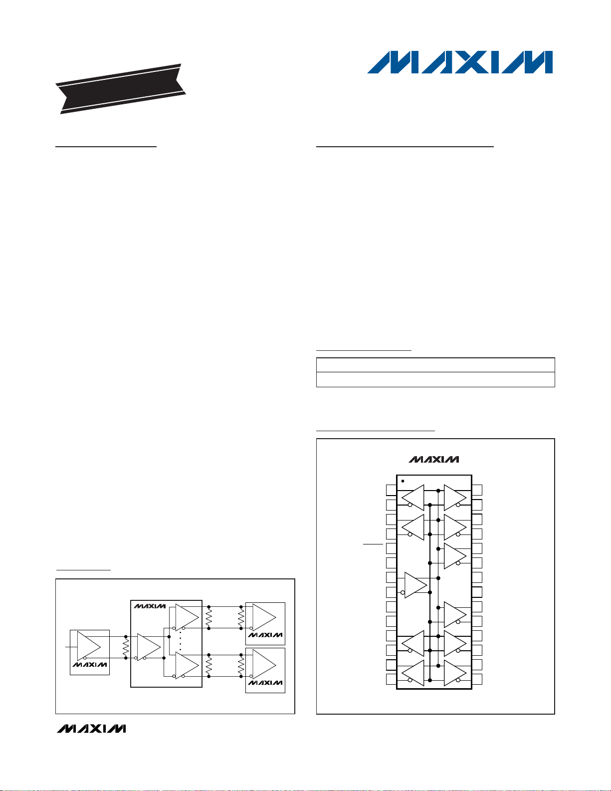
Typical Application Circuit
28
27
26
25
24
23
22
21
20
19
18
17
16
15
1
2
3
4
5
6
7
8
9
10
11
12
13
14
DO3+
DO3-
DO4+
DO4-
DO5+
DO5-
DO8-
V
CC
GND
DO6+
DO6-
DO7+
DO7-
DO8+
DO9-
DO9+
DO10-
DO10+
V
CC
GND
RIN-
RIN+
GND
DO1-
DO1+
DO2-
DO2+
TOP VIEW
MAX9150
PWRDN
TSSOP
Pin Configuration
General Description
The MAX9150 low-jitter, 10-port, low-voltage differential
signaling (LVDS) repeater is designed for applications
that require high-speed data or clock distribution while
minimizing power, space, and noise. The device
accepts a single LVDS input and repeats the signal at
10 LVDS outputs. Each differential output drives a total
of 50Ω, allowing point-to-point distribution of signals on
transmission lines with 100Ω terminations on each end.
Ultra-low 120ps (max) peak-to-peak jitter (deterministic
and random) ensures reliable communication in highspeed links that are highly sensitive to timing error,
especially those incorporating clock-and-data recovery,
or serializers and deserializers. The high-speed switching performance guarantees 400Mbps data rate and
less than 100ps skew between channels while operating from a single +3.3V supply.
Supply current at 400Mbps is 160mA (max) and is
reduced to 60µA (max) in low-power shutdown mode.
Inputs and outputs conform to the EIA/TIA-644 LVDS
standard. A fail-safe feature sets the outputs high when
the input is undriven and open, terminated, or shorted.
The MAX9150 is available in a 28-pin TSSOP package.
Refer to the MAX9110/MAX9112 and MAX9111/MAX9113
data sheets for LVDS line drivers and receivers.
________________________Applications
Cellular Phone Base Stations
Add/Drop Muxes
Digital Crossconnects
Network Switches/Routers
Backplane Interconnect
Clock Distribution
Features
♦ Ultra-Low 120ps
p-p
(max) Total Jitter
(Deterministic and Random)
♦ 100ps (max) Skew Between Channels
♦ Guaranteed 400Mbps Data Rate
♦ 60µA Shutdown Supply Current
♦ Conforms to EIA/TIA-644 LVDS Standard
♦ Single +3.3V Supply
♦ Fail-Safe Circuit Sets Output High for Undriven
Inputs
♦ High-Impedance LVDS Input when V
CC
= 0V
For price, delivery, and to place orders, please contact Maxim Distribution at 1-888-629-4642,
or visit Maxim’s website at www.maxim-ic.com.
PART TEMP. RANGE PIN-PACKAGE
MAX9150EUI -40°C to +85°C 28 TSSOP
LVDS
T
100Ω
X
MAX9110
MAX9150
1
10
LVDS
100Ω
BACKPLANE
OR CABLE
100Ω 100Ω
100Ω
R
X
MAX9111
R
X
MAX9111
Page 2
MAX9150
Low-Jitter, 10-Port LVDS Repeater
2 _______________________________________________________________________________________
ABSOLUTE MAXIMUM RATINGS
DC ELECTRICAL CHARACTERISTICS
(VCC= +3.0V to +3.6V, RL= 50Ω ±1%, |V
ID|
= 0.1V to 1.0V, VCM= |VID/ 2|to 2.4V - |VID/ 2|, PWRDN = high, TA= -40°C to +85°C,
unless otherwise noted. Typical values are at V
CC
= +3.3V, TA= +25°C.) (Note 1)
Stresses beyond those listed under “Absolute Maximum Ratings” may cause permanent damage to the device. These are stress ratings only, and functional
operation of the device at these or any other conditions beyond those indicated in the operational sections of the specifications is not implied. Exposure to
absolute maximum rating conditions for extended periods may affect device reliability.
VCCto GND...........................................................-0.3V to +4.0V
RIN+, RIN- to GND ................................................-0.3V to +4.0V
PWRDN to GND..........................................-0.3V to (V
CC
+ 0.3V)
DO_+, DO_- to GND..............................................-0.3V to +4.0V
Short-Circuit Duration (DO_+, DO_-) .........................Continuous
Continuous Power Dissipation (T
A
= +70°C)
28-Pin TSSOP (derate 12.8mW/°C above +70°C) .....1026mW
Storage Temperature.........................................-65°C to +150°C
Maximum Junction Temperature .....................................+150°C
Operating Temperature Range...........................-40°C to +85°C
Lead Temperature (soldering, 10s) .................................+300°C
)
PARAMETER SYMBOL CONDITIONS MIN TYP MAX UNITS
P W R D N
Input High Voltage V
Input Low Voltage V
Input Current I
LVDS INPUT
Differential Input High Threshold V
Differential Input Low Threshold V
Single-Ended Input Current I
Power-Off Single-Ended Input
Current
Differential Input Resistance RI
LVDS DRIVER
Differential Output Voltage V
Change in VOD Between
Complementary Output States
Offset (Common-Mode) Voltage V
Change in VOS Between
Complementary Output States
Output High Voltage V
Output Low Voltage V
Differential Output Resistance
(Note 2)
Differential High Output Voltage
in Fail-Safe
Output Short-Circuit Current I
IH
IL
VIN = VCC and 0V -15 15 µA
IN
TH
TL
PWRDN = high or low; V
RIN-
= open or RIN+ = open, V
IN
I
IN(OFF
DIFF
OD
ΔV
OD
OS
ΔV
OS
OH
OL
RO
DIFFVCC
V
OD+
SC
PWRDN = high or low; V
RIN-
= open or RIN+ = open, V
V
= 0V; V
CC
or RIN+
= open, V
VCC = +3.6V or 0V, PWRDN = high or low 5 kΩ
Figure 1 250 320 450 mV
Figure 1 25 mV
Figure 1 0.90 1.25 1.375 V
Figure 1 25 mV
Figure 1 1.6 V
Figure 1 0.7 V
= +3.6V or 0V, PWRDN = high or low 150 240 330 Ω
R
, R
IN+
undriven with short, open, or
IN-
100Ω termination
VID = +100mV, V
VID = -100mV, V
2.0 V
7 100 mV
-100 -7 mV
= 2.4V,
RIN+
RIN+
= 2.4V, RIN- = open
RIN+
= 2.4V
RIN-
RIN-
= 0V,
RIN-
= 2.4V
= 0V
-6 +1
-18 +1
-1 +12 µA
250 450 mV
= GND
DO_+
DO_-
= GND
-15 mA
0.8 V
µA
Page 3
MAX9150
Low-Jitter, 10-Port LVDS Repeater
_______________________________________________________________________________________ 3
DC ELECTRICAL CHARACTERISTICS (continued)
(VCC= +3.0V to +3.6V, RL= 50Ω ±1%, |V
ID|
= 0.1V to 1.0V, VCM= |VID/ 2|to 2.4V - |VID/ 2|, PWRDN = high, TA= -40°C to +85°C,
unless otherwise noted. Typical values are at V
CC
= +3.3V, TA= +25°C.) (Note 1)
AC ELECTRICAL CHARACTERISTICS
(VCC= +3.0V to +3.6V, RL= 50Ω ±1%, CL= 5pF, |V
ID|
= 0.2V to 1.0V, VCM= |VID/ 2|to 2.4V - |VID/ 2|, PWRDN = high, TA= -40°C
to +85°C, unless otherwise noted. Typical values are at V
CC
= +3.3V, TA= +25°C.) (Notes 2–5)
p-p
PARAMETER SYMBOL CONDITIONS MIN TYP MAX UNITS
Single-Ended Output HighImpedance Current
SUPPLY CURRENT
Supply Current (Note 2) I
Power-Down Supply Current I
VCC = 0V, PWRDN = GND;
V
= 3.6V or 0V, DO_- = open; or
DO_+
= 3.6V or 0V, DO_+ = open
V
I
OZ
CC
CCZ
DO_-
PWRDN = GND;
= 3.6V or 0V, DO_- = open; or
V
DO_+
V
= 3.6V or 0V, DO_+ = open
DO_-
DC 100 140
200MHz (400Mbps)
PWRDN = GND 60 µA
PARAMETER SYMBOL CONDITIONS MIN TYP MAX UNITS
Differential Propagation Delay
High-to-Low
Differential Propagation Delay
Low-to-High
t
PHLD
t
PLHD
Figures 2, 3 1.6 2.2 3.5 ns
Figures 2, 3 1.6 2.2 3.5 ns
Figure 2
-1 +1 µA
-1 +1 µA
130 160
mA
Total Peak-to-Peak Jitter
(Random and Deterministic)
(Note 6)
Differential Output-to-Output
Skew (Note 7)
Differential Part-to-Part Skew
(Note 8)
Rise/Fall Time T
M axi m um Inp ut Fr eq uency ( N ote 9) f
TLH, tTHL
t
JPP
t
SKOO
t
SKPP
MAX
Figures 2, 3 20 120 ps
Figures 2, 3 40 100 ps
Figures 2, 3 1.9 ns
Figures 2, 3 150 220 450 ps
Figures 2, 3 400 Mbps
Page 4

MAX9150
Low-Jitter, 10-Port LVDS Repeater
4 _______________________________________________________________________________________
Typical Operating Characteristics
(Figure 2, VCC= +3.3V, RL= 50Ω, CL= 5pF, IVIDI = 200mV, VCM= 1.2V, fIN= 50MHz, TA = +25°C, unless otherwise noted.)
SUPPLY CURRENT (mA)
150
90
0.1 1 100 1000
SUPPLY CURRENT vs. FREQUENCY
100
120
110
130
140
MAX9150 toc01
INPUT FREQUENCY (MHz)
10
2.10
2.20
2.15
2.30
2.25
2.35
2.40
3.0 3.2 3.33.1 3.4 3.5 3.6
DIFFERENTIAL PROPAGATION DELAY
vs. SUPPLY VOLTAGE
MAX9150 toc02
VCC (V)
DIFFERENTIAL PROPAGATION DELAY (ns)
t
PHLD
t
PLHD
50 7060 80 90 100
MAX9150 toc03
RL (Ω)
2.10
2.20
2.15
2.30
2.25
2.35
2.40
DIFFERENTIAL PROPAGATION DELAY
vs. OUTPUT LOAD
DIFFERENTIAL PROPAGATION DELAY (ns)
t
PLHD
t
PHLD
Note 1: Current-into-device pins is defined as positive. Current-out-of-device pins is defined as negative. All voltages are
referenced to ground, except V
TH
, VTL, VOD, and ΔVOD.
Note 2: Guaranteed by design, not production tested.
Note 3: AC parameters are guaranteed by design and characterization.
Note 4: C
L
includes scope probe and test jig capacitance.
Note 5: Signal generator conditions, unless otherwise noted: frequency = 200MHz, 50% duty cycle, R
O
= 50Ω, tR= 1ns, and tF=
1ns (0% to 100%).
Note 6: Signal generator conditions for t
JPP
: VOD= 200mV, VOS= 1.2V, frequency = 200MHz, 50% duty cycle, RO= 50Ω, tR= 1ns,
and t
F
= 1ns (0% to 100%. t
JPP
includes pulse (duty cycle) skew.
Note 7: t
SKOO
is the magnitude difference in differential propagation delay between outputs for a same-edge transition.
Note 8: t
SKPP
is the |MAX - MIN|differential propagation delay.
Note 9: Device meets V
OD
and AC specifications while operating at f
MAX
.
AC ELECTRICAL CHARACTERISTICS (continued)
(VCC= +3.0V to +3.6V, RL= 50Ω ±1%, CL= 5pF, |V
ID|
= 0.2V to 1.0V, VCM= |VID/ 2|to 2.4V - |VID/ 2|, PWRDN = high, TA= -40°C
to +85°C, unless otherwise noted. Typical values are at V
CC
= +3.3V, TA= +25°C.) (Notes 2–5)
PARAMETER SYMBOL CONDITIONS MIN TYP MAX UNITS
Power-Down Time t
Power-Up Time t
PD
PU
Figures 4, 5
100 ns
100 µs
Page 5

MAX9150
Low-Jitter, 10-Port LVDS Repeater
_______________________________________________________________________________________
5
Typical Operating Characteristics (continued)
(Figure 2, VCC= +3.3V, RL= 50Ω, CL= 5pF, IVIDI = 200 mV, VCM= 1.2V, fIN= 50MHz, TA = +25°C, unless otherwise noted.)
50 7060 80 90 100
DIFFERENTIAL OUTPUT vs. OUTPUT LOAD
RL (Ω)
270
370
320
470
420
520
570
MAX9150 toc10
DIFFERENTIAL OUTPUT (mV)
310
315
325
320
330
335
3.0 3.23.1 3.3 3.4 3.5 3.6
DIFFERENTIAL OUTPUT vs. SUPPLY VOLTAGE
MAX9150 toc09
VCC (V)
DIFFERENTIAL OUTPUT (mV)
DIFFERENTIAL PROPAGATION DELAY
vs. COMMON-MODE VOLTAGE
2.50
2.45
2.40
2.35
t
2.30
2.25
2.20
2.15
DIFFERENTIAL PROPAGATION DELAY (ns)
2.10
t
PHLD
0 0.5 1.0 1.5 2.0 2.5
PLHD
VCM (V)
240
230
220
210
200
TRANSITION TIME (ps)
190
MAX9150 toc04
TRANSITION TIME vs. OUTPUT LOAD
t
TLH
DIFFERENTIAL OUTPUT-TO-OUTPUT
SKEW vs. SUPPLY VOLTAGE
40
H
30
G
20
B
A, E
10
F, I
D
0
C
-10
DIFFERENTIAL OUTPUT-TO-OUTPUT SKEW (ps)
-20
3.0 3.23.1 3.3 3.4 3.5 3.6
t
THL
A = D02 - D01 B = D03 - D01 C = D04 - D01
D = D05 - D01 E = D06 - D01 F = D07 - D01
G = D08 - D01 H = D09 - D01 I = D010 - D01
VCC (V)
600
MAX9150 toc07
500
400
300
TRANSITION TIME (ps)
200
TRANSITION TIME vs. SUPPLY VOLTAGE
215
210
MAX9150 toc05
205
200
195
TRANSITION TIME (ps)
190
185
3.0 3.2 3.33.1 3.4 3.5 3.6
TRANSITION TIME vs. CAPACITANCE
t
TLH
t
THL
t
THL
VCC (V)
MAX9150 toc08
t
TLH
MAX9150 toc06
180
50 7060 80 90 100
RL (Ω)
100
597111315
CL (pF)
Page 6

Detailed Description
The LVDS interface standard is a signaling method
intended for point-to-point communication over a controlled impedance medium, as defined by the
ANSI/TIA/EIA-644 and IEEE 1596.3 standards. The
LVDS standard uses a lower voltage swing than other
common communication standards, achieving higher
data rates with reduced power consumption while
reducing EMI emissions and system susceptibility to
noise.
The MAX9150 is a 400Mbps, 10-port LVDS repeater
intended for high-speed, point-to-point, low-power
applications. This device accepts an LVDS input and
repeats it on 10 LVDS outputs. The device is capable of
detecting differential signals as low as 100mV and as
high as 1V within a 0 to 2.4V input voltage range. The
LVDS standard specifies an input voltage range of 0 to
2.4V referenced to ground.
The MAX9150 outputs use a current-steering configuration to generate a 5mA to 9mA output current. This current-steering approach induces less ground bounce
and no shoot-through current, enhancing noise margin
and system speed performance. The driver outputs are
short-circuit current limited, and are high impedance
(to ground) when PWRDN = low or the device is not
powered. The outputs have a typical differential resistance of 240Ω.
The MAX9150 current-steering architecture requires a
resistive load to terminate the signal and complete the
transmission loop. Because the device switches the
direction of current flow and not voltage levels, the output voltage swing is determined by the total value of
the termination resistors multiplied by the output current. With a typical 6.4mA output current, the MAX9150
produces a 320mV output voltage when driving a transmission line terminated at each end with a 100Ω termi-
nation resistor (6.4mA x 50Ω = 320mV). Logic states
are determined by the direction of current flow through
the termination resistors.
Fail-Safe
Fail-safe is a receiver feature that puts the output in a
known logic state (high) under certain fault conditions.
The MAX9150 outputs are differential high when the
inputs are undriven and open, terminated, or shorted
(Table 1).
MAX9150
Low-Jitter, 10-Port LVDS Repeater
6 _______________________________________________________________________________________
Table 1. Input/Output Function Table
Note: VID= RIN+ - RIN-, VOD= DO_+ - DO_-
High = 450mV > V
OD
> 250mV
Low = -250mV > V
OD
> -450mV
Pin Description
PIN NAME FUNCTION
1, 3, 11, 13,
16, 18, 20,
24, 26, 28
2, 4, 12, 14,
15, 17, 19,
23, 25, 27
5 PWRDN
6, 9, 21 GND Ground
DO2+, DO1+, DO10+,
DO9+, DO8+, DO7+,
DO6+, DO5+, DO4+, DO3+
DO2-, DO1-, DO10-, DO9-,
DO8-, DO7-,
DO6-, DO5-, DO4-, DO3-
Differential LVDS Outputs. Connect a 100Ω resistor across each of the output
pairs (DO_+ and DO_-) adjacent to the IC, and connect a 100Ω resistor at the
input of the receiving circuit.
Power Down. Drive PWRDN low to disable all outputs and reduce supply current
to 60µA. Drive PWRDN high for normal operation.
10, 22 V
7 RIN+
8 RIN-
CC
Power. Bypass each VCC pin to GND with 0.1µF and 1nF ceramic capacitors.
LVDS Receiver Inputs. RIN+ and RIN- are high-impedance inputs. Connect a
resistor from RIN+ to RIN- to terminate the input signal.
INPUT, V
+100mV High
-100mV Low
Open High
Short High
Terminated
ID
Undriven
OUTPUTS, V
High
OD
Page 7

MAX9150
Low-Jitter, 10-Port LVDS Repeater
_______________________________________________________________________________________ 7
Applications Information
Supply Bypassing
Bypass each of the VCCpins with high-frequency surface-mount ceramic 0.1µF and 1nF capacitors in parallel as close to the device as possible, with the smaller
valued capacitor closest to the V
CC
pins.
Differential Traces
Output trace characteristics affect the performance of
the MAX9150. Use controlled impedance traces to
match trace impedance to both the transmission medium impedance and termination resistor. Ensure that
noise couples as common mode by running the differential traces close together. Reduce skew by matching
the electrical length of the traces. Excessive skew can
result in a degradation of magnetic field cancellation.
Maintain the distance between the differential traces to
avoid discontinuities in differential impedance. Avoid
90° turns and minimize the number of vias to further
prevent impedance discontinuities.
Cables and Connectors
Transmission media should have a controlled differential impedance of 100Ω. Use cables and connectors
that have matched differential impedance to minimize
impedance discontinuities.
Avoid the use of unbalanced cables, such as ribbon or
simple coaxial cable. Balanced cables, such as twisted
pair, offer superior signal quality and tend to generate
less EMI due to canceling effects. Balanced cables
tend to pick up noise as common mode, which is
rejected by the LVDS receiver.
Termination
Termination resistors should match the differential characteristic impedance of the transmission line. Since the
MAX9150 has current-steering devices, an output voltage will not be generated without a termination resistor.
Output voltage levels are dependent upon the value of
the total termination resistance. The MAX9150 produces LVDS output levels for point-to-point links that
are double terminated (100Ω at each end). With the
typical 6.4mA output current, the MAX9150 produces
an output voltage of 320mV when driving a transmission line terminated at each end with a 100Ω termina-
tion resistor (6.4mA x 50Ω = 320mV). Termination
resistance values may range between 90Ω and 150Ω,
depending on the characteristic impedance of the
transmission medium.
Minimize the distance between the output termination
resistor and the corresponding MAX9150 transmitter
output. Use ±1% surface-mount resistors.
Minimize the distance between the input termination
resistor and the MAX9150 receiver input. Use a ±1%
surface-mount resistor.
Chip Information
PROCESS : CMOS
Figure 1. Driver-Load Test Circuit
Test Circuits and Timing Diagrams
GENERATOR
50Ω
50Ω
RIN+
RIN-
MAX9150
DO1+
25Ω
V
OD
25Ω
25Ω
V
OD
25Ω
DO1-
DO10+
DO10-
V
OS
V
OS
Page 8

MAX9150
Low-Jitter, 10-Port LVDS Repeater
8 _______________________________________________________________________________________
Test Circuits and Timing Diagrams (continued)
Figure 3. Propagation Delay and Transition Time Waveforms
Figure 2. Repeater Propagation Delay and Transition Time Test Circuit
C
L
5pF
C
5pF
L
50Ω
MAX9150
R
L
50Ω
DO1+
DO1-
50Ω
RIN+
RIN-
GENERATOR
R
IN-
0
V
CM
R
IN+
DIFFERENTIAL
t
PLHD
80%
50% O O 50%
20%
t
TLH
C
L
5pF
C
L
5pF
V
ID
80%
V
= (V
) - (V
DIFF
DO_+
DO_-
)
R
L
50Ω
V
t
CM
PHLD
t
THL
DO10+
DO10-
20%
Page 9

MAX9150
Low-Jitter, 10-Port LVDS Repeater
_______________________________________________________________________________________ 9
Figure 4. Power-Up/Down Delay Test Circuit
Figure 5. Power-Up/Down Delay Waveform
Test Circuits and Timing Diagrams (continued)
PACKAGE TYPE PACKAGE CODE DOCUMENT NO.
28 TSSOP U28-4
21-0066
Package Information
For the latest package outline information and land patterns, go to www.maxim-ic.com/packages. Note that a “+”, “#”, or “-” in the
package code indicates RoHS status only. Package drawings may show a different suffix character, but the drawing pertains to the
package regardless of RoHS status.
1.1V
1.0V
1.1V
1.0V
GENERATOR
RIN+
RIN-
PWRDN
C
50Ω
MAX9150
5pF
C
5pF
C
5pF
C
5pF
L
L
L
L
R
25Ω
R
25Ω
R
25Ω
R
25Ω
DO1+
L
L
DO1-
DO10+
L
L
DO10-
1.2V
1.2V
50%
50%
3.0V
O
V
1.2V
1.2V
V
OH
OL
PWRDN
V
WHEN VID = +100mV
DO_+
WHEN VID = -100mV
V
DO_-
V
WHEN VID = -100mV
DO_+
WHEN VID = +100mV
V
DO_-
1.5V
t
t
1.5V
t
PD
50%
50%
PD
PU
t
PU
Page 10

MAX9150
Low-Jitter, 10-Port LVDS Repeater
Maxim cannot assume responsibility for use of any circuitry other than circuitry entirely embodied in a Maxim product. No circuit patent licenses are
implied. Maxim reserves the right to change the circuitry and specifications without notice at any time.
10
____________________Maxim Integrated Products, 120 San Gabriel Drive, Sunnyvale, CA 94086 408-737-7600
© 2009 Maxim Integrated Products Maxim is a registered trademark of Maxim Integrated Products, Inc.
Revision History
REVISION
NUMBER
0 10/00 Initial release —
1 3/09
REVISION
DATE
DESCRIPTION
Replaced the obsolete Rev C package outline drawing with the Package Information
table
PAGES
CHANGED
9
 Loading...