

Page 1
General Description
The MAX9129 is a quad bus low-voltage differential signaling (BLVDS) driver with flow-through pinout. This
device is designed to drive a heavily loaded multipoint
bus with controlled transition times (1ns 0% to 100%
minimum) for reduced reflections. The MAX9129
accepts four LVTTL/LVCMOS input levels and translates them to output levels of 250mV to 450mV (standard LVDS levels) into a 27Ω load at speeds up to
200Mbps (100MHz).
The power-on reset ensures that all four outputs are
disabled and high impedance during power up and
power down. The outputs can be set to high impedance by two enable inputs, EN and EN, thus dropping
the device to a low-power state of 11mW. The enables
are common to all four drivers. The flow-through pinout
simplifies PC board layout and reduces crosstalk by
keeping the LVTTL/LVCMOS inputs and BLVDS outputs
separated.
The MAX9129 operates from a single +3.3V supply and
is specified for operation from -40°C to +85°C. It is
available in 16-pin QFN and TSSOP packages. Refer to
the MAX9121 data sheet for a quad LVDS line receiver
with flow-through pinout.
Applications
Cell Phone Base Stations
Add/Drop Muxes
Digital Cross-Connects
DSLAMs
Network Switches/Routers
Backplane Interconnect
Clock Distribution
Features
♦ Drive LVDS Levels into a 27Ω Load
♦ 1ns (0% to 100%) Minimum Transition Time
Reduces Reflections
♦ Guaranteed 200Mbps (100MHz) Data Rate
♦ Enable Pins for High-Impedance Output
♦ High-Impedance Outputs when Powered Off
♦ Glitch-Free Power-Up and Power-Down
♦ Hot Swappable
♦ Flow-Through Pinout
♦ Available in Tiny QFN Package (50% Smaller
than TSSOP)
♦ Single +3.3V Supply
MAX9129
Quad Bus LVDS Driver with
Flow-Through Pinout
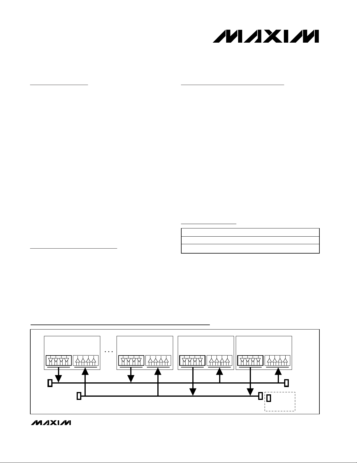
MAX9129 MAX9121 MAX9129 MAX9121 MAX9129 MAX9121 MAX9129 MAX9121
R
t
R
t
R
t
BUS A
BUS B
R
t
CARD 1A CARD 10A CARD 1B CARD 2B
= TERMINATION
RESISTOR
R
t
MULTIPOINT FULL-DUPLEX TRANSMIT AND RECEIVE BUS
Typical Applications Circuit
19-2100; Rev 0; 8/01
For pricing, delivery, and ordering information, please contact Maxim/Dallas Direct! at
1-888-629-4642, or visit Maxim’s website at www.maxim-ic.com.
Functional Diagram appears at end of data sheet.
Pin Configurations appear at end of data sheet.
Ordering Information
________________________________________________________________ Maxim Integrated Products 1
PART TEMP. RANGE PIN-PACKAGE
MAX9129EGE -40°C to +85°C 16 QFN
MAX9129EUE -40°C to +85°C 16 TSSOP
Page 2
MAX9129
Quad Bus LVDS Driver with
Flow-Through Pinout
2 _______________________________________________________________________________________
ABSOLUTE MAXIMUM RATINGS
Stresses beyond those listed under “Absolute Maximum Ratings” may cause permanent damage to the device. These are stress ratings only, and functional
operation of the device at these or any other conditions beyond those indicated in the operational sections of the specifications is not implied. Exposure to
absolute maximum rating conditions for extended periods may affect device reliability.
VCCto GND...........................................................-0.3V to +4.0V
IN_, EN, EN to GND....................................-0.3V to (V
CC
+ 0.3V)
OUT_+, OUT_- to GND..........................................-0.3V to +4.0V
Short-Circuit Duration (OUT_+, OUT_-) .....................Continuous
Continuous Power Dissipation (T
A
= +70°C)
16-Pin QFN (derate 18.5mW/°C above +70°C) .........1481mW
16-Pin TSSOP (derate 9.4mW/°C above +70°C) .........755mW
Storage Temperature Range .............................-65°C to +150°C
Maximum Junction Temperature .....................................+150°C
Operating Temperature Range ...........................-40°C to +85°C
ESD Protection
Human Body Model, OUT_+, OUT_- ...............................±8kV
Lead Temperature (soldering, 10s) .................................+300°C
DC ELECTRICAL CHARACTERISTICS
(VCC= +3.0V to +3.6V, RL= 27Ω ±1%, EN = high, EN = low, TA= -40°C to +85°C, unless otherwise noted. Typical values are at V
CC
= +3.3V, TA= +25°C.) (Notes 1, 2)
BLVDS OUTPUTS (OUT_+, OUT_-)
Differential Output Voltage V
Change in Magnitude of V
Between Complementary Output
States
Offset Voltage V
Change in Magnitude of V
Between Complementary Output
States
Output High Voltage V
Output Low Voltage V
Differential Output Short-Circuit
Current
Output Short-Circuit Current I
Output High-Impedance Current I
Power-Off Output Current I
PARAMETER SYMBOL CONDITIONS MIN TYP MAX UNITS
Figure 1 250 371 450 mV
Figure 1 1 25 mV
OD
Figure 1 1.125 1.29 1.375 V
OS
Figure 1 5 25 mV
OS
OL
VOD = 0 20 mA
OUT_+ = 0 at IN_ = VCC or
OUT_- = 0 at IN_ = 0
Disabled, OUT_+ = 0 or VCC, OUT_- = 0
or V
CC
VCC = 0 or open, EN = EN = IN_ = 0,
OUT_+ = 0 or 3.6V, OUT_- = 0 or 3.6V
OD
OS
∆V
I
OD
∆V
OH
OSD
OS
OZ
OFF
1.465 1.6 V
0.90 1.085 V
-20 mA
-1 1 µA
-1 1 µA
Output Capacitance C
INPUTS (IN_, EN, EN)
High-Level Input Voltage V
Low-Level Input Voltage V
Input Current I
SUPPLY CURRENT
Supply Current I
Disabled Supply Current I
OUT
IN
CC
CCZ
C ap aci tance fr om OU T_+ or O U T_- to G N D 4.3 pF
IH
IL
IN_, EN, EN = 0 or V
RL = 27Ω, IN_ = VCC or 0 for all channels 58 70 mA
Disabled 3.2 5 mA
CC
2.0 V
GND 0.8 V
-15 15 µA
CC
V
Page 3
MAX9129
Quad Bus LVDS Driver with
Flow-Through Pinout
_______________________________________________________________________________________ 3
AC ELECTRICAL CHARACTERISTICS
(VCC= +3.0V to +3.6V, RL= 27Ω ±1%, CL= 15pF, EN = high, EN = low, TA= -40°C to +85°C, unless otherwise noted. Typical values
are at V
CC
= +3.3V, TA= +25°C.) (Notes 3, 4, 5)
Note 1: Maximum and minimum limits over temperature are guaranteed by design and characterization. Devices are 100% tested
at T
A
= +25°C.
Note 2: Current into the device is defined as positive, and current out of the device is defined as negative. All voltages are
referenced to ground except V
OD
and ∆VOD.
Note 3: AC parameters are guaranteed by design and characterization.
Note 4: C
L
includes probe and jig capacitance.
Note 5: Signal generator conditions: V
OL
= 0, VOH= VCC, f = 100MHz, 50% duty cycle, RO= 50Ω, tR= tF= 1ns (10% to 90%).
Note 6: t
SKD1
is the magnitude difference of differential propagation delays. t
SKD1
= | t
PHLD
- t
PLHD |
.
Note 7: t
SKD2
is the magnitude difference of t
PHLD
or t
PLHD
of one channel to the t
PHLD
or t
PLHD
of another channel on the
same device.
Note 8: t
SKD3
is the magnitude difference of any differential propagation delays between devices at the same VCCand within 5°C
of each other.
Note 9: t
SKD4
is the magnitude difference of any differential propagation delays between devices operating over the rated supply
and temperature ranges.
Note 10: Signal generator conditions: V
OL
= 0, VOH= VCC, f = 100MHz, 50% duty cycle, RO= 50Ω, tR= tF= 1ns (10% to 90%).
MAX9129 output criteria: duty cycle = 45% to 55%, V
OD
≥ 250mV, all channels switching.
Differential Propagation Delay
High to Low
Differential Propagation Delay
Low to High
Differential Pulse Skew (Note 6) t
Differential Channel-to-Channel
Skew (Note 7)
Differential Part-to-Part Skew
(Note 8)
Differential Part-to-Part Skew
(Note 9)
Rise Time t
Fall Time t
Disable Time High to Z t
Disable Time Low to Z t
Enable Time Z to High t
Enable Time Z to Low t
Maximum Operating Frequency
(Note 10)
PARAMETER SYMBOL CONDITIONS MIN TYP MAX UNITS
t
PHLD
t
PLHD
SKD1
t
SKD2
t
SKD3
t
SKD4
TLH
THL
PHZ
PLZ
PZH
PZL
f
MAX
Figures 2 and 3 1.0 1.98 3.0 ns
Figures 2 and 3 1.0 1.92 3.0 ns
Figures 2 and 3 300 ps
Figures 2 and 3 450 ps
Figures 2 and 3 1.2 ns
Figures 2 and 3 2.0 ns
Figures 2 and 3
Figures 2 and 3
Figures 4 and 5 8 ns
Figures 4 and 5 8 ns
Figures 4 and 5 10 ns
Figures 4 and 5 10 ns
Figure 2 100 MHz
MAX9129EGE 0.60 1.19 1.55
MAX9129EUE 0.60 1.09 1.40
MAX9129EGE 0.60 1.12 1.55
MAX9129EUE 0.60 1.02 1.40
ns
ns
Page 4
MAX9129
Quad Bus LVDS Driver with
Flow-Through Pinout
4 _______________________________________________________________________________________
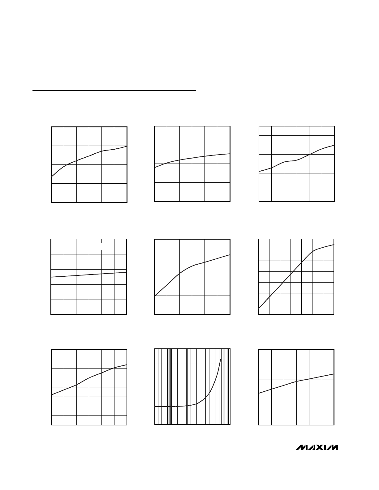
Typical Operating Characteristics
(MAX9129EUE (TSSOP package), VCC= +3.3V, RL= 27Ω, CL = 15pF, TA= +25°C, unless otherwise noted.) (Note 5)
1.48
1.47
1.46
1.45
1.44
3.0 3.3 3.6
OUTPUT HIGH VOLTAGE
vs. SUPPLY VOLTAGE
MAX9129 toc01
SUPPLY VOLTAGE (V)
OUTPUT HIGH VOLTAGE (V)
1.12
1.10
1.08
1.06
1.04
3.0 3.3 3.6
OUTPUT LOW VOLTAGE
vs. SUPPLY VOLTAGE
MAX9129 toc02
SUPPLY VOLTAGE (V)
OUTPUT LOW VOLTAGE (V)
-14.08
-14.09
-14.10
-14.11
-14.12
3.0 3.3 3.6
OUTPUT SHORT CURRENT (IOS)
vs. SUPPLY VOLTAGE
MAX9129 toc03
SUPPLY VOLTAGE (V)
OUTPUT SHORT CURRENT (mA)
420
422
426
424
428
430
3.0 3.3 3.6
OUTPUT HIGH-IMPEDANCE CURRENT
vs. SUPPLY VOLTAGE
MAX9129 toc04
SUPPLY VOLTAGE (V)
OUTPUT HIGH-IMPEDANCE CURRENT (pA)
V
OUT_
= VCC OR 0
372.0
371.5
371.0
370.5
370.0
3.0 3.3 3.6
DIFFERENTIAL OUTPUT VOLTAGE vs.
SUPPLY VOLTAGE
MAX9129 toc05
SUPPLY VOLTAGE (V)
DIFFERENTIAL OUTPUT VOLTAGE (mV)
0
0.500
0.250
1.000
0.750
1.500
1.250
1.750
10 50 7030 90 110 130 150
DIFFERENTIAL OUTPUT VOLTAGE
vs. LOAD RESISTANCE
MAX9129 toc06
LOAD RESISTANCE (Ω)
DIFFERENTIAL OUTPUT VOLTAGE (V)
1.265
1.270
1.275
1.280
1.285
1.290
1.295
1.300
1.305
3.0 3.3 3.6
OUTPUT OFFSET VOLTAGE
vs. SUPPLY VOLTAGE
MAX9129 toc07
SUPPLY VOLTAGE (V)
OUTPUT OFFSET VOLTAGE (V)
55
57
61
59
63
65
0101 1000
SUPPLY CURRENT
vs. FREQUENCY
MAX9129 toc08
FREQUENCY (MHz)
SUPPLY CURRENT (mA)
100
56.7
56.9
57.3
57.1
57.5
57.7
3.0 3.3 3.6
SUPPLY CURRENT
vs. SUPPLY VOLTAGE
MAX9129 toc09
SUPPLY VOLTAGE (V)
SUPPLY CURRENT (mA)
Page 5

MAX9129
Quad Bus LVDS Driver with
Flow-Through Pinout
_______________________________________________________________________________________ 5
Typical Operating Characteristics (continued)
(MAX9129EUE (TSSOP package), VCC= +3.3V, RL= 27Ω, CL = 15pF, TA= +25°C, unless otherwise noted.) (Note 5)
0.800
0.900
0.850
1.050
1.000
0.950
1.200
1.150
1.100
1.250
-40 10-15 35 60 85
TRANSITION TIME
vs. TEMPERATURE
MAX9129 toc16
TRANSITION TIME (ns)
t
TLH
t
THL
20% TO 80%
60
59
58
57
SUPPLY CURRENT (mA)
56
55
-40 10-15 35 60 85
70
60
50
40
SUPPLY CURRENT
vs. TEMPERATURE
TEMPERATURE (°C)
DIFFERENTIAL SKEW
vs. SUPPLY VOLTAGE
DIFFERENTIAL PROPAGAION DELAY
vs. SUPPLY VOLTAGE
2.10
2.05
MAX9129 toc10
2.00
1.95
1.90
1.85
DIFFERENTIAL PROPAGATION DELAY (ns)
1.80
3.0 3.3 3.6
SUPPLY VOLTAGE (V)
DIFFERENTIAL SKEW
vs. TEMPERATURE
MAX9129 toc13
100
80
60
t
PLHD
t
PHLD
DIFFERENTIAL PROPAGATION DELAY
vs. TEMPERATURE
2.20
2.10
MAX9129 toc11
2.00
1.90
1.80
1.70
DIFFERENTIAL PROPAGATION DELAY (ns)
1.60
-40 10-15 35 60 85
TRANSITION TIME
vs. SUPPLY VOLTAGE
1.3
MAX9129 toc14
1.2
1.1
t
PHLD
TEMPERATURE (°C)
t
TLH
t
PLHD
20% TO 80%
MAX9129 toc12
MAX9129 toc15
30
20
DIFFERENTIAL SKEW (ps)
10
0
3.0 3.3 3.6
SUPPLY VOLTAGE (V)
40
DIFFERENTIAL SKEW (ps)
20
0
-40 10-15 35 60 85
TEMPERATURE (°C)
1.0
TRANSITION TIME (ns)
0.9
0.8
3.0 3.3 3.6
SUPPLY VOLTAGE (V)
t
THL
Page 6
MAX9129
Quad Bus LVDS Driver with
Flow-Through Pinout
6 _______________________________________________________________________________________
Pin Description
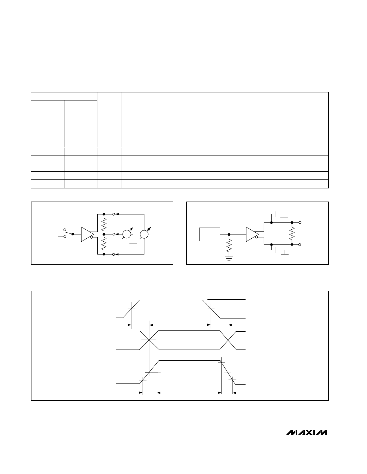
Figure 3. Driver Propagation Delay and Transition Time Waveforms
Figure 1. Driver VODand VOSTest Circuit
Figure 2. Driver Propagation Delay and Transition Time Test
Circuit
PIN
QFN TSSOP
NAME FUNCTION
LVTTL/LVCMOS Enable Input. The driver is disabled when EN is low. EN is internally
15 1 EN
pulled down. When EN = high and EN = low or open, the outputs are active. For other
combinations of EN and EN, the outputs are disabled and are high impedance.
1, 4, 5, 16 2, 3, 6, 7 IN_ LVTTL/LVCMOS Driver Inputs
24V
CC
Power-Supply Input. Bypass VCC to GND with 0.1µF and 0.001µF ceramic capacitors.
3 5 GND Ground
68EN
LVTTL/LVCMOS Enable Input. The driver is disabled when EN is high. EN is internally
pulled down.
7, 10, 11, 14 9, 12, 13, 16 OUT_- Inverting BLVDS Driver Outputs
8, 9, 12, 13 10, 11, 14, 15 OUT_+ Noninverting BLVDS Driver Outputs
OUT_+
R
/2
V
GND
CC
IN_
L
OS
V
/2
R
L
OUT_-
V
V
OS
OD
GENERATOR
50Ω
IN_
C
L
OUT_ +
R
L
OUT_ -
C
L
V
CC
OUT_
80%
-)
50%
t
PHLD
0
V
OH
0
V
OL
0
20%
t
THL
OUT_
OUT_+
V
IN_
50%
t
20%
PLHD
t
TLH
0 DIFFERENTIAL
80%
V
0
OD
= (V
OUT_
+) - (V
-
OD
Page 7

Detailed Description
The MAX9129 is a 200Mbps quad differential BLVDS
driver designed for multipoint, heavily loaded backplane
applications. This device accepts LVTTL/LVCMOS input
levels and translates them to output levels of 250mV to
450mV into a 27Ω load. The flow-through pinout simplifies board layout and reduces the potential for crosstalk
between single-ended inputs and differential outputs.
Transition times are designed to reduce reflections, yet
enable high data rates. The MAX9129 can be used in
conjunction with standard quad LVDS receivers, such
as the MAX9121, to implement full-duplex multipoint
buses more efficiently than with transceivers.
Effect of Capacitive Loading
The characteristic impedance of a differential PC board
trace is uniformly reduced when equal capacitive loads
are attached at equal intervals (provided the transition
time of the signal being driven on the trace is longer
than the delay between loads). This kind of loading is
typical of multipoint buses where cards are attached at
1in or 0.8in intervals along the length of a backplane.
MAX9129
Quad Bus LVDS Driver with
Flow-Through Pinout
_______________________________________________________________________________________ 7
Table 1. Input/Output Function Table
Figure 4. Driver High-Impedance Delay Test Circuit
Figure 5. Driver High-Impedance Delay Waveform
C
L
V
GENERATOR
CC
GND
EN
EN
50Ω
IN_
1/4 MAX9129
C
L
EN WHEN EN = 0 OR OPEN
EN WHEN EN = V
OUT_+ WHEN IN_ = V
OUT_- WHEN IN_ = 0
CC
CC
RL/2
R
OUT_+
+1.2V
/2
L
OUT_-
50%
50%
t
PHZ
ENABLES INPUTS OUTPUTS
EN EN IN_ OUT_+ OUT_ -
H L or open
All other combinations of
EN and EN
50%
50%
t
PZH
LLH
HHL
XZZ
V
CC
0
V
CC
0
V
OH
50%50%
1.2V
OUT_+ WHEN IN_ = 0
OUT_- WHEN IN_ = V
CC
t
PLZ
1.2V
50%50%
V
t
PZL
OL
Page 8

MAX9129
The reduction in characteristic impedance is approximated by the following formula:
Z
DIFF-loaded
= Z
DIFF-unloaded
✕
SQRT [Co/ (Co+ N
✕
CL/ L)]
where:
Z
DIFF-unloaded
= unloaded differential characteristic im-
pedance
Co= unloaded trace capacitance (pF/unit length)
CL= value of each capacitive load (pF)
N = number of capacitive loads
L = trace length
For example, if Co= 2.5pF/in, CL= 10pF, N = 18, L =
18in, and Z
DIFF-unloaded
= 120Ω, the loaded differential
impedance is:
Z
DIFF-loaded
= 120Ω✕SQRT [2.5pF /
(2.5pF + 18 ✕10pF/18in)]
Z
DIFF-loaded
= 54Ω
In this example, capacitive loading reduces the characteristic impedance from 120Ω to 54Ω. The load seen by
a driver located on a card in the middle of the bus is
27Ω because the driver sees two 54Ω loads in parallel.
A typical LVDS driver (rated for a 100Ω load) would not
develop a large enough differential signal to be reliably
detected by an LVDS receiver. Maxim’s BLVDS driver is
designed and specified to drive a 27Ω load to differential voltage levels of 250mV to 450mV (which are standard LVDS driver levels). A standard LVDS receiver is
able to detect this level of differential signal.
Short extensions off the bus, called stubs, contribute to
capacitive loading. Keep stubs less than 1in for a good
balance between ease of component placement and
good signal integrity.
The MAX9129 is a current source driver and drives
larger differential signal levels into loads higher than
27Ω and smaller levels into loads less than 27Ω (see
typical operating curves). To keep loading from reducing bus impedance below the rated 27Ω load, PC
board traces can be designed for higher unloaded
characteristic impedance.
Effect of Transition Time
For transition times (measured from 0% to 100%) shorter than the delay between capacitive loads, the loads
are seen as low-impedance discontinuities from which
the driven signal is reflected. Reflections add and subtract from the signal being driven and cause decreased
noise margin and jitter. The MAX9129 is designed for a
minimum transition time of 1ns (rated 0.6ns from 20% to
80%, or about 1ns 0% to 100%) to reduce reflections
while being fast enough for high-speed backplane data
transmission.
Power-On Reset
The power-on reset voltage of the MAX9129 is typically
2.25V. When the supply falls below this voltage, the
device is disabled and the outputs are in high impedance.
Applications Information
Power-Supply Bypassing
Bypass VCCwith high-frequency, surface-mount
ceramic 0.1µF and 0.001µF capacitors in parallel as
close to the device as possible, with the smaller valued
capacitor closest to VCC.
Termination
In the example above, the loaded differential impedance of the bus is reduced to 54Ω. Since it can be driven from any card position, the bus must be terminated
at each end. A parallel termination of 54Ω at each end
of the bus placed across the traces that make up the
differential pair provides a proper termination. The total
load seen by the driver is 27Ω.
The MAX9129 drives higher differential signal levels
into lighter loads. A multidrop bus with the driver at one
end and receivers connected at regular intervals along
the bus has a lowered impedance due to capacitive
loading. Assuming the same impedance calculated in
the multidrop example above (54Ω), the multidrop bus
can be terminated with a single, parallel-connected
54Ω resistor at the far end from the driver. Only a single
resistor is required because the driver sees one 54Ω
differential trace. The signal swing is larger with a 54Ω
load.
In general, parallel terminate each end of the bus with a
resistor matching the differential impedance of the bus
(taking into account any reduced impedance due to
loading).
Board Layout
A four-layer PC board that provides separate power,
ground, input, and output signals is recommended.
Keep the LVTTL/LVCMOS and BLVDS signals separated to prevent coupling as shown in the suggested layout for the QFN package (not drawn to scale) (Figure 6).
Quad Bus LVDS Driver with
Flow-Through Pinout
8 _______________________________________________________________________________________
Page 9

Chip Information
TRANSISTOR COUNT: 948
PROCESS: CMOS
MAX9129
Quad Bus LVDS Driver with
Flow-Through Pinout
_______________________________________________________________________________________ 9
Figure 6. Suggested Layout for QFN Package
EN
IN1
IN2
V
CC
GND
IN3
IN4
EN
GND
OUT1-
OUT1+
OUT2+
OUT2-
OUT3-
OUT3+
OUT4+
OUT4-
Page 10

MAX9129
Quad Bus LVDS Driver with
Flow-Through Pinout
10 ______________________________________________________________________________________
Pin Configurations
OUT1+
OUT1-
OUT2+
OUT2-
OUT3+
OUT3-
OUT4+
OUT4-
EN
EN
IN1
IN2
IN3
IN4
MAX9129
Functional Diagram
TOP VIEW
16
15
OUT1+
14
OUT2+
13
OUT2-
12
OUT3-
OUT3+
11
10
OUT4+
9
OUT4-
EN OUT1-
1
IN1
2
IN2
3
MAX9129
4
V
CC
GND
5
IN3
6
IN4
7
EN
8
TSSOP
V
GND
IN2
IN3
CC
GND
1
2
3
4
GND
EN
IN1
16
MAX9129
5
IN4
(4mm x 4mm)
(CONTACTS UNDER QFN)
EN
QFN
15
GND
6
OUT1-
OUT4-
OUT1+
14
7
OUT4+
GND
13
12
OUT2+
OUT2-
11
OUT3-
10
9
OUT3+
8
GND
Page 11

MAX9129
Quad Bus LVDS Driver with
Flow-Through Pinout
______________________________________________________________________________________ 11
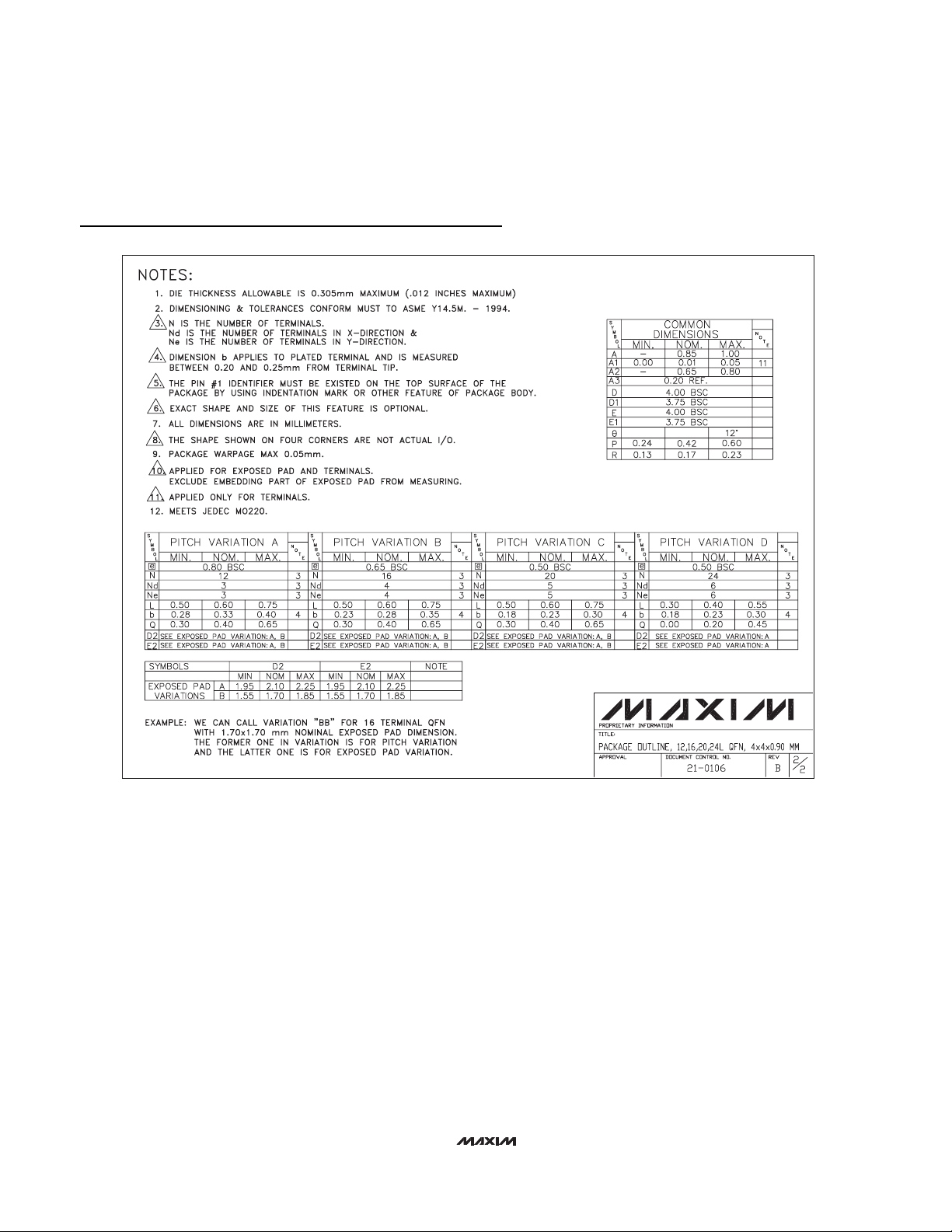
Package Information
TSSOP,NO PADS.EPS
Page 12
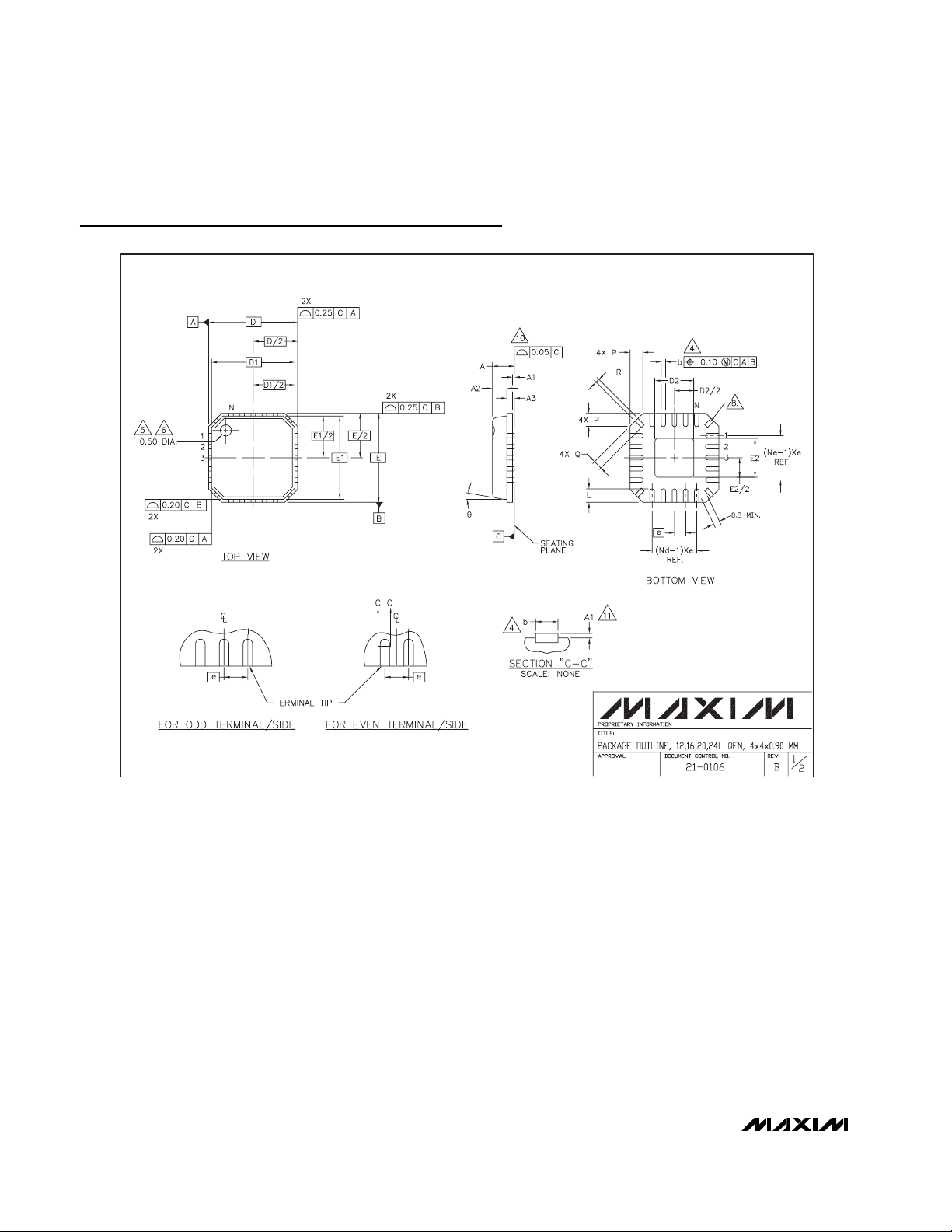
MAX9129
Quad Bus LVDS Driver with
Flow-Through Pinout
12 ______________________________________________________________________________________
Package Information (continued)
12, 16,20, 24L QFN.EPS
Page 13
MAX9129
Quad Bus LVDS Driver with
Flow-Through Pinout
Maxim cannot assume responsibility for use of any circuitry other than circuitry entirely embodied in a Maxim product. No circuit patent licenses are
implied. Maxim reserves the right to change the circuitry and specifications without notice at any time.
Maxim Integrated Products, 120 San Gabriel Drive, Sunnyvale, CA 94086 408-737-7600 ____________________ 13
© 2001 Maxim Integrated Products Printed USA is a registered trademark of Maxim Integrated Products.
Package Information (continued)
 Loading...