

Page 1
General Description
The MAX9123 quad low-voltage differential signaling
(LVDS) differential line driver is ideal for applications
requiring high data rates, low power, and low noise. The
MAX9123 is guaranteed to transmit data at speeds up to
800Mbps (400MHz) over controlled impedance media of
approximately 100Ω. The transmission media may be
printed circuit (PC) board traces, backplanes, or cables.
The MAX9123 accepts four LVTTL/LVCMOS input levels
and translates them to LVDS output signals. Moreover,
the MAX9123 is capable of setting all four outputs to a
high-impedance state through two enable inputs, EN and
EN, thus dropping the device to an ultra-low-power state
of 16mW (typ) during high impedance. The enables are
common to all four transmitters. Outputs conform to the
ANSI TIA/EIA-644 LVDS standard. Flow-through pinout
simplifies PC board layout and reduces crosstalk by separating the LVTTL/LVCMOS inputs and LVDS outputs.
The MAX9123 operates from a single +3.3V supply and is
specified for operation from -40°C to +85°C. It is available
in 16-pin TSSOP and SO packages. Refer to the MAX9121/
MAX9122* data sheet for quad LVDS line receivers with
integrated termination and flow-through pinout.
Applications
Features
♦ Flow-Through Pinout
Simplifies PC Board Layout
Reduces Crosstalk
♦ Pin Compatible with DS90LV047A
♦ Guaranteed 800Mbps Data Rate
♦ 250ps Maximum Pulse Skew
♦ Conforms to TIA/EIA-644 LVDS Standard
♦ Single +3.3V Supply
♦ 16-Pin TSSOP and SO Packages
MAX9123
Quad LVDS Line Driver with
Flow-Through Pinout
________________________________________________________________ Maxim Integrated Products 1
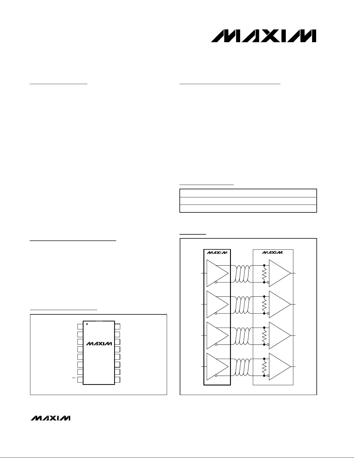
Pin Configuration
Ordering Information
107Ω
MAX9123
MAX9122*
107Ω
107Ω
107Ω
R
X
LVDS SIGNALS
100Ω SHIELDED TWISTED CABLE OR MICROSTRIP PC BOARD TRACES
LVTTL/CMOS
DATA INPUT
LVTTL/CMOS
DATA OUTPUT
R
X
R
X
R
X
T
X
T
X
T
X
T
X
Typical Applications Circuit
19-1927; Rev 0; 2/01
For price, delivery, and to place orders, please contact Maxim Distribution at 1-888-629-4642,
or visit Maxim’s website at www.maxim-ic.com.
* Future product—contact factory for availability.
Digital Copiers
Laser Printers
Cell Phone Base
Stations
Add Drop Muxes
Digital Cross-Connects
DSLAMs
Network
Switches/Routers
Backplane
Interconnect
Clock Distribution
PART TEMP. RANGE PIN-PACKAGE
MAX9123EUE -40°C to +85°C 16 TSSOP
MAX9123ESE -40°C to +85°C 16 SO
TOP VIEW
1
EN OUT1-
IN1
2
V
GND
IN2
IN3
IN4
CC
EN
3
4
5
6
7
8
MAX9123
TSSOP/SO
16
15
14
13
12
11
10
9
OUT1+
OUT2+
OUT2-
OUT3-
OUT3+
OUT4+
OUT4-
Page 2
MAX9123
Quad LVDS Line Driver with
Flow-Through Pinout
2 _______________________________________________________________________________________
ABSOLUTE MAXIMUM RATINGS
DC ELECTRICAL CHARACTERISTICS
(VCC= +3.0V to +3.6V, RL= 100Ω ±1%, TA= -40°C to +85°C. Typical values are at VCC= +3.3V, TA= +25°C, unless otherwise
noted.) (Notes 1, 2)
Stresses beyond those listed under “Absolute Maximum Ratings” may cause permanent damage to the device. These are stress ratings only, and functional
operation of the device at these or any other conditions beyond those indicated in the operational sections of the specifications is not implied. Exposure to
absolute maximum rating conditions for extended periods may affect device reliability.
VCCto GND...........................................................-0.3V to +4.0V
IN_, EN, EN to GND....................................-0.3V to (V
CC
+ 0.3V)
OUT_+, OUT_- to GND..........................................-0.3V to +3.9V
Short-Circuit Duration (OUT_+, OUT_-) .....................Continuous
Continuous Power Dissipation (T
A
= +70°C)
16-Pin TSSOP (derate 9.4mW/°C above +70°C) .........755mW
16-Pin SO (derate 8.7mW/°C above +70°C)................696mW
Storage Temperature Range .............................-65°C to +150°C
Maximum Junction Temperature .....................................+150°C
Operating Temperature Range ...........................-40°C to +85°C
Lead Temperature (soldering, 10s) .................................+300°C
ESD Protection
Human Body Model, IN_, OUT_+, OUT_-.......................±4kV
PARAMETER
SYMBOL
CONDITIONS
MIN
TYP
MAX
UNITS
LVDS OUTPUT (OUT_+, OUT_-)
Differential Output Voltage V
OD
Figure 1
368 450 mV
Change in Magnitude of V
OD
Between Complementary Output
States
∆V
OD
Figure 1 1 35 mV
Offset Voltage V
OS
Figure 1
V
Change in Magnitude of V
OS
Between Complementary Output
States
∆V
OS
Figure 1 4 25 mV
Output High Voltage V
OH
1.6 V
Output Low Voltage V
OL
V
Differential Output Short-Circuit
Current (Note 3)
I
OSD
Enabled, VOD = 0 -9 mA
Output Short-Circuit Current I
OS
OUT_+ = 0 at IN_ = VCC or OUT_- = 0 at IN_
= 0, enabled
-9 mA
Output High-Impedance Current
I
OZ
OUT_- = 0 or VCC , RL = ∞
-10 10 µA
Power-Off Output Current I
OFF
VCC = 0 or open, OUT_+ = 0 or 3.6V, OUT_= 0 or 3.6V, R
L
= ∞
-20 20 µA
INPUTS (IN_, EN, EN)
High-Level Input Voltage V
IH
2.0
V
Low-Level Input Voltage V
IL
0.8 V
Input Current I
IN
IN_, EN, EN = 0 or V
CC
-20 20 µA
SUPPLY CURRENT
No-Load Supply Current I
CC
RL = ∞, IN_ = VCC or 0 for all channels 9.2 11 mA
Loaded Supply Current I
CCL
RL = 100Ω, IN_ = VCC or 0 for all channels
30 mA
Disabled Supply Current I
CCZ
D i sab l ed , IN _ = V
C C
or 0 for all channel s,
E N = 0, EN = V
CC
4.9 6 mA
250
1.125 1.25 1.375
EN = low and EN = high, OUT_+ = 0 or VCC,
0.90
-3.8
GND
22.7
V
CC
Page 3
MAX9123
Quad LVDS Line Driver with
Flow-Through Pinout
_______________________________________________________________________________________ 3
SWITCHING CHARACTERISTICS
(VCC= +3.0V to +3.6V, RL= 100Ω ±1%, CL= 15pF, TA= -40°C to +85°C. Typical values are at VCC= +3.3V, TA= +25°C, unless
otherwise noted.) (Notes 4, 5, 6)
Note 1: Maximum and minimum limits over temperature are guaranteed by design and characterization. Devices are 100% tested
at T
A
= +25°C.
Note 2: Currents into the device are positive, and current out of the device is negative. All voltages are referenced to ground except
V
OD
.
Note 3: Guaranteed by correlation data.
Note 4: AC parameters are guaranteed by design and characterization.
Note 5: C
L
includes probe and jig capacitance.
Note 6: Signal generator conditions for dynamic tests: V
OL
= 0, VOH= 3V, f = 100MHz, 50% duty cycle, RO= 50Ω, tR≤ 1ns, tF≤
1ns (0% to 100%).
Note 7: t
SKD1
is the magnitude difference of differential propagation delay. t
SKD1
= |t
PHLD
- t
PLHD
|.
Note 8: t
SKD2
is the magnitude difference of t
PHLD
or t
PLHD
of one channel to the t
PHLD
or t
PLHD
of another channel on the same
device.
Note 9: t
SKD3
is the magnitude difference of any differential propagation delays between devices at the same VCCand within 5°C
of each other.
Note 10: t
SKD4
is the magnitude difference of any differential propagation delays between devices operating over the rated supply
and temperature ranges.
Note 11: f
MAX
signal generator conditions: VOL= 0, VOH= 3V, f = 400MHz, 50% duty cycle, RO= 50Ω, tR≤ 1ns, tF≤ 1ns (0% to
100%). Transmitter output criteria: duty cycle = 45% to 55%, V
OD
≥ 250mV.
Differential Propagation Delay
High to Low
Differential Propagation Delay
Low to High
Differential Pulse Skew (Note 7) t
Differential Channel-to-Channel
Skew (Note 8)
Differential Part-to-Part Skew
(Note 9)
Differential Part-to-Part Skew
(Note 10)
Rise Time t
Fall Time t
Disable Time High to Z t
Disable Time Low to Z t
Enable Time Z to High t
Enable Time Z to Low t
Maximum Operating Frequency
(Note 11)
PARAMETER SYMBOL CONDITIONS MIN TYP MAX UNITS
t
PHLD
t
PLHD
SKD1
t
SKD2
t
SKD3
t
SKD4
TLH
THL
PHZ
PLZ
PZH
PZL
f
MAX
Figures 2 and 3 0.7 1.7 ns
Figures 2 and 3 0.7 1.7 ns
Figures 2 and 3 0.04 0.25 ns
Figures 2 and 3 0.07 0.35 ns
Figures 2 and 3 0.13 0.8 ns
Figures 2 and 3
Figures 2 and 3 0.2 0.39 1.0 ns
Figures 2 and 3 0.2 0.39 1.0 ns
Figures 4 and 5 2.7 5 ns
Figures 4 and 5 2.7 5 ns
Figures 4 and 5 2.3 7 ns
Figures 4 and 5 2.3 7 ns
400 MHz
0.43 1.0 ns
Page 4
MAX9123
Quad LVDS Line Driver with
Flow-Through Pinout
4 _______________________________________________________________________________________
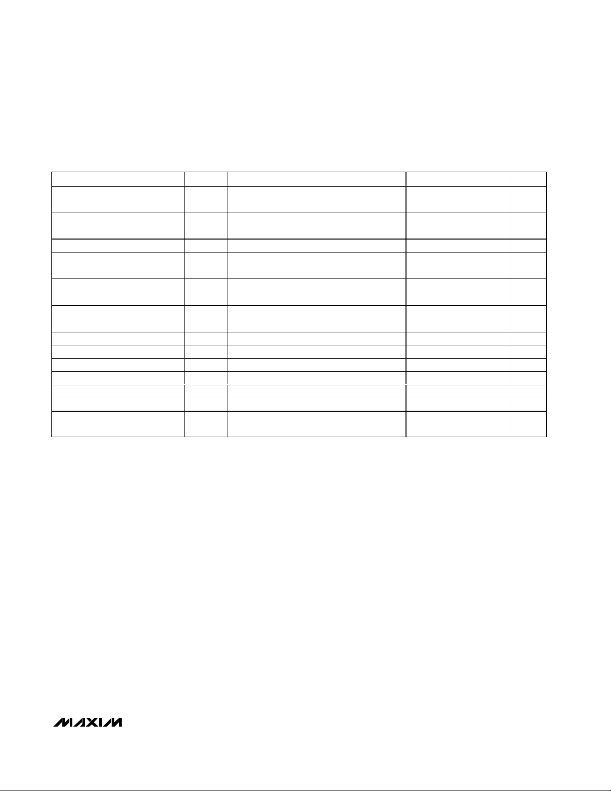
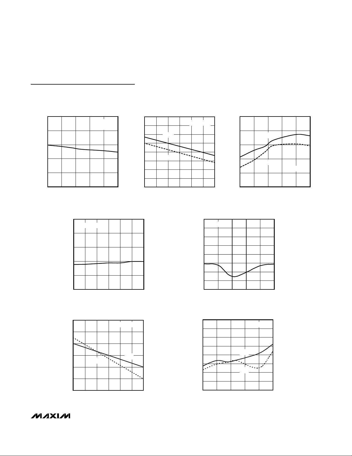
Typical Operating Characteristics
(VCC= +3.3V, RL= 100Ω, CL= 15pF, TA= +25°C, unless otherwise noted.)
1.090
1.094
1.092
1.098
1.096
1.100
3.0 3.3 3.6
OUTPUT HIGH VOLTAGE
vs. POWER-SUPPLY VOLTAGE
MAX9123 toc01
POWER-SUPPLY VOLTAGE (V)
OUTPUT HIGH VOLTAGE (V)
1.090
1.092
1.096
1.094
1.098
1.100
3.0 3.3 3.6
OUTPUT LOW VOLTAGE
vs. POWER-SUPPLY VOLTAGE
MAX9123 toc02
POWER-SUPPLY VOLTAGE (V)
OUTPUT LOW VOLTAGE (V)
-3.650
-3.665
-3.660
-3.655
-3.670
-3.675
-3.680
-3.685
-3.690
-3.695
-3.700
3.0 3.3 3.6
OUTPUT SHORT-CIRCUIT CURRENT
vs. POWER-SUPPLY VOLTAGE
MAX9123 toc03
OUTPUT SHORT-CIRCUIT CURRENT (mA)
POWER-SUPPLY VOLTAGE (V)
VIN = VCC or
GND
-250
-200
-100
-150
-50
0
3.0 3.3 3.6
MAX9123 toc04
OUTPUT HIGH-IMPEDANCE STATE CURRENT
vs. POWER-SUPPLY VOLTAGE
OUTPUT HIGH-IMPEDANCE STATE CURRENT (pA)
POWER-SUPPLY VOLTAGE (V)
VIN = VCC or
GND
350
355
360
365
370
375
380
385
390
3.0 3.3 3.6
DIFFERENTIAL OUTPUT VOLTAGE
vs. POWER SUPPLY
MAX9123 toc05
POWER-SUPPLY VOLTAGE (V)
DIFFERENTIAL OUTPUT VOLTAGE (V)
300
400
350
500
450
550
600
90 110 120100 130 140 150
DIFFERENTIAL OUTPUT VOLTAGE
vs. LOAD RESISTOR
MAX9123 toc06
LOAD RESISTOR (Ω)
DIFFERENTIAL OUTPUT VOLTAGE (mV)
1.240
1.244
1.252
1.248
1.256
1.260
3.0 3.3 3.6
OFFSET VOLTAGE
vs. POWER-SUPPLY VOLTAGE
MAX9123 toc07
POWER-SUPPLY VOLTAGE (V)
OFFSET VOLTAGE (V)
40
20
0.1 10 1001 1000
POWER-SUPPLY CURRENT
vs. FREQUENCY
MAX9123 toc08
FREQUENCY (MHz)
POWER-SUPPLY CURRENT (mA)
23
25
28
30
33
35
38
VIN = 0 to 3V
ALL SWITCHING
ONE SWITCHING
20.0
22.0
21.0
23.0
24.0
25.0
3.0 3.3 3.6
POWER-SUPPLY CURRENT
vs. POWER-SUPPLY VOLTAGE
MAX9123 toc09
POWER-SUPPLY VOLTAGE (V)
POWER-SUPPLY CURRENT (mA)
FREQ = 1MHz
V
IN
= 0 to 3V
Page 5
MAX9123
Quad LVDS Line Driver with
Flow-Through Pinout
_______________________________________________________________________________________ 5
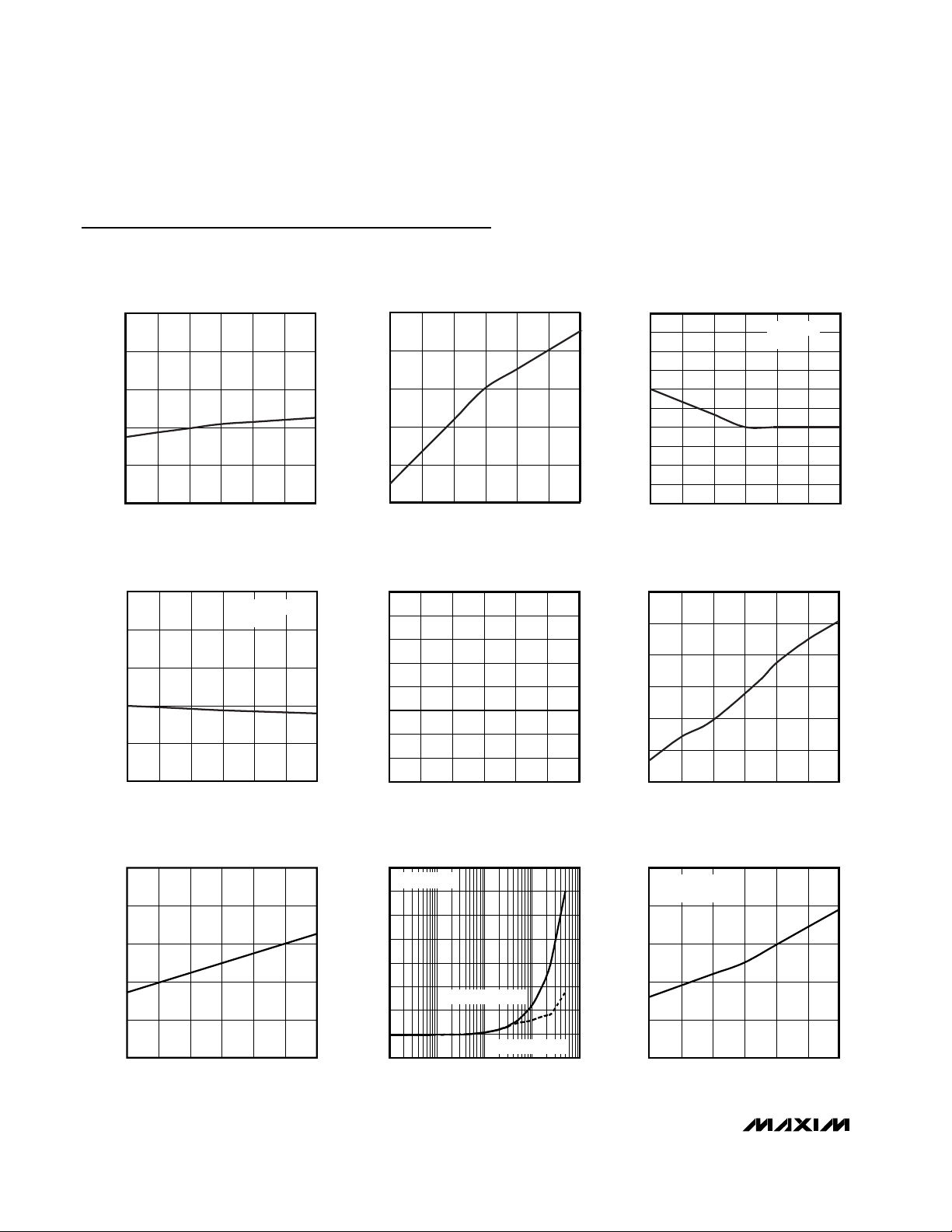
Typical Operating Characteristics (continued)
(VCC= +3.3V, RL= 100Ω, CL= 15pF, TA= +25°C, unless otherwise noted.)
POWER-SUPPLY CURRENT
vs. AMBIENT TEMPERATURE
25.0
24.0
23.0
22.0
POWER-SUPPLY CURRENT (mA)
21.0
20.0
-40 10-15 356085
AMBIENT TEMPERATURE (°C)
FREQ = 1MHz
= 0 to 3V
V
IN
DIFFERENTIAL SKEW
vs. POWER-SUPPLY VOLTAGE
100
FREQ = 1MHz
80
60
40
DIFFERENTIAL SKEW (ps)
20
0
3.0 3.3 3.6
POWER-SUPPLY VOLTAGE (V)
TRANSITION TIME
vs. POWER-SUPPLY VOLTAGE
400
390
380
370
360
TRANSITION TIME (ps)
350
340
3.0 3.3 3.6
t
THL
POWER-SUPPLY VOLTAGE (V)
MAX9123 toc10
FREQ = 1MHz
t
TLH
DIFFERENTIAL PROPAGATION DELAY
vs. POWER SUPPLY
1.600
1.550
1.500
1.450
1.400
1.350
1.300
1.250
DIFFERENTIAL PROPAGATION DELAY (ns)
1.200
3.0 3.3 3.6
MAX9123 toc13
MAX9123 toc15
t
PLHD
t
PHLD
POWER-SUPPLY VOLTAGE (V)
DIFFERENTIAL PROPAGATION DELAY
vs. AMBIENT TEMPERATURE
1.600
FREQ = 1MHz
MAX9123 toc11
1.500
1.400
1.300
1.200
DIFFERENTIAL PROPAGATION DELAY (ns)
1.100
-40 10-15 356085
DIFFERENTIAL SKEW
vs. AMBIENT TEMPERATURE
200
FREQ = 1MHz
175
150
125
100
75
DIFFERENTIAL SKEW (ps)
50
25
0
-40 10-15 35 60 85
AMBIENT TEMPERATURE (°C)
TRANSITION TIME
vs. AMBIENT TEMPERATURE
600
550
500
450
400
350
TRANSITION TIME (ps)
300
250
200
-40 -15 10 35 60 85
AMBIENT TEMPERATURE (°C)
FREQ = 1MHz
t
TLH
t
THL
t
PLHD
t
PHLD
FREQ = 1MHz
AMBIENT TEMPERATURE (°C)
MAX9123 toc14
MAX9123 toc16
MAX9123 toc12
Page 6

MAX9123
Quad LVDS Line Driver with
Flow-Through Pinout
6 _______________________________________________________________________________________
Pin Description
Detailed Description
The LVDS interface standard is a signaling method
intended for point-to-point communication over a controlled-impedance medium as defined by the
ANSI/TIA/EIA-644 and IEEE 1596.3 standards. The
LVDS standard uses a lower voltage swing than other
common communication standards, achieving higher
data rates with reduced power consumption while
reducing EMI emissions and system susceptibility to
noise.
The MAX9123 is an 800Mbps quad differential LVDS
driver that is designed for high-speed, point-to-point,
and low-power applications. This device accepts
LVTTL/LVCMOS input levels and translates them to
LVDS output signals.
The MAX9123 generates a 2.5mA to 4.0mA output current using a current-steering configuration. This currentsteering approach induces less ground bounce and no
shoot-through current, enhancing noise margin and system speed performance. The driver outputs are shortcircuit current limited, and enter a high-impedance state
when the device is not powered or is disabled.
The current-steering architecture of the MAX9123
requires a resistive load to terminate the signal and
complete the transmission loop. Because the device
switches current and not voltage, the actual output voltage swing is determined by the value of the termination
resistor at the input of an LVDS receiver. Logic states
are determined by the direction of current flow through
the termination resistor. With a typical 3.7mA output
current, the MAX9123 produces an output voltage of
370mV when driving a 100Ω load.
Termination
Because the MAX9123 is a current-steering device, no
output voltage will be generated without a termination
resistor. The termination resistors should match the differential impedance of the transmission line. Output
voltage levels depend upon the value of the termination
resistor. The MAX9123 is optimized for point-to-point
interface with 100Ω termination resistors at the receiver
inputs. Termination resistance values may range
between 90Ω and132Ω, depending on the characteristic impedance of the transmission medium.
Applications Information
Power-Supply Bypassing
Bypass VCCwith high-frequency, surface-mount
ceramic 0.1µF and 0.001µF capacitors in parallel as
close to the device as possible, with the smaller valued
capacitor closest to VCC.
Differential Traces
Output trace characteristics affect the performance of
the MAX9123. Use controlled-impedance traces to
match trace impedance to the transmission medium.
Table 1. Input/Output Function Table
PIN NAME FUNCTION
Driver Enable Input. The driver is disabled when EN is low. EN is internally pulled down. When EN =
1EN
2, 3, 6, 7 IN_ LVTTL/LVCMOS Driver Inputs
4VCCPower-Supply Input. Bypass VCC to GND with 0.1µF and 0.001µF ceramic capacitors.
5 GND Ground
8 EN Driver Enable Input. The transmitter is disabled when EN is high. EN is internally pulled down.
9, 12, 13, 16 OUT_- Inverting LVDS Driver Outputs
10, 11, 14, 15 OUT_+ Noninverting LVDS Driver Outputs
high and EN = low or open, the outputs are active. For other combinations of EN and EN, the
outputs are disabled and are high impedance.
ENABLES INPUTS OUTPUTS
EN EN IN_ OUT_+ OUT_ -
H L or open L L H
H L or open H H L
All other combinations
of ENABLE pins
Don’t
care
ZZ
Page 7
MAX9123
Quad LVDS Line Driver with
Flow-Through Pinout
_______________________________________________________________________________________ 7
Eliminate reflections and ensure that noise couples as
common mode by running the differential trace pairs
close together. Reduce skew by matching the electrical
length of the traces. Excessive skew can result in a
degradation of magnetic field cancellation.
Maintain the distance between the differential traces to
avoid discontinuities in differential impedance. Avoid
90° turns and minimize the number of vias to further
prevent impedance discontinuities.
Cables and Connectors
Transmission media should have a nominal differential
impedance of 100Ω. To minimize impedance discontinuities, use cables and connectors that have matched
differential impedance.
Avoid the use of unbalanced cables such as ribbon or
simple coaxial cable. Balanced cables such as twisted
pair offer superior signal quality and tend to generate
less EMI due to canceling effects. Balanced cables
tend to pick up noise as common mode, which is
rejected by the LVDS receiver.
Board Layout
For LVDS applications, a four-layer PC board that provides separate power, ground, LVDS signals, and input
signals is recommended. Isolate the LVTTL/LVCMOS
and LVDS signals from each other to prevent coupling.
Chip Information
TRANSISTOR COUNT: 1246
PROCESS: CMOS
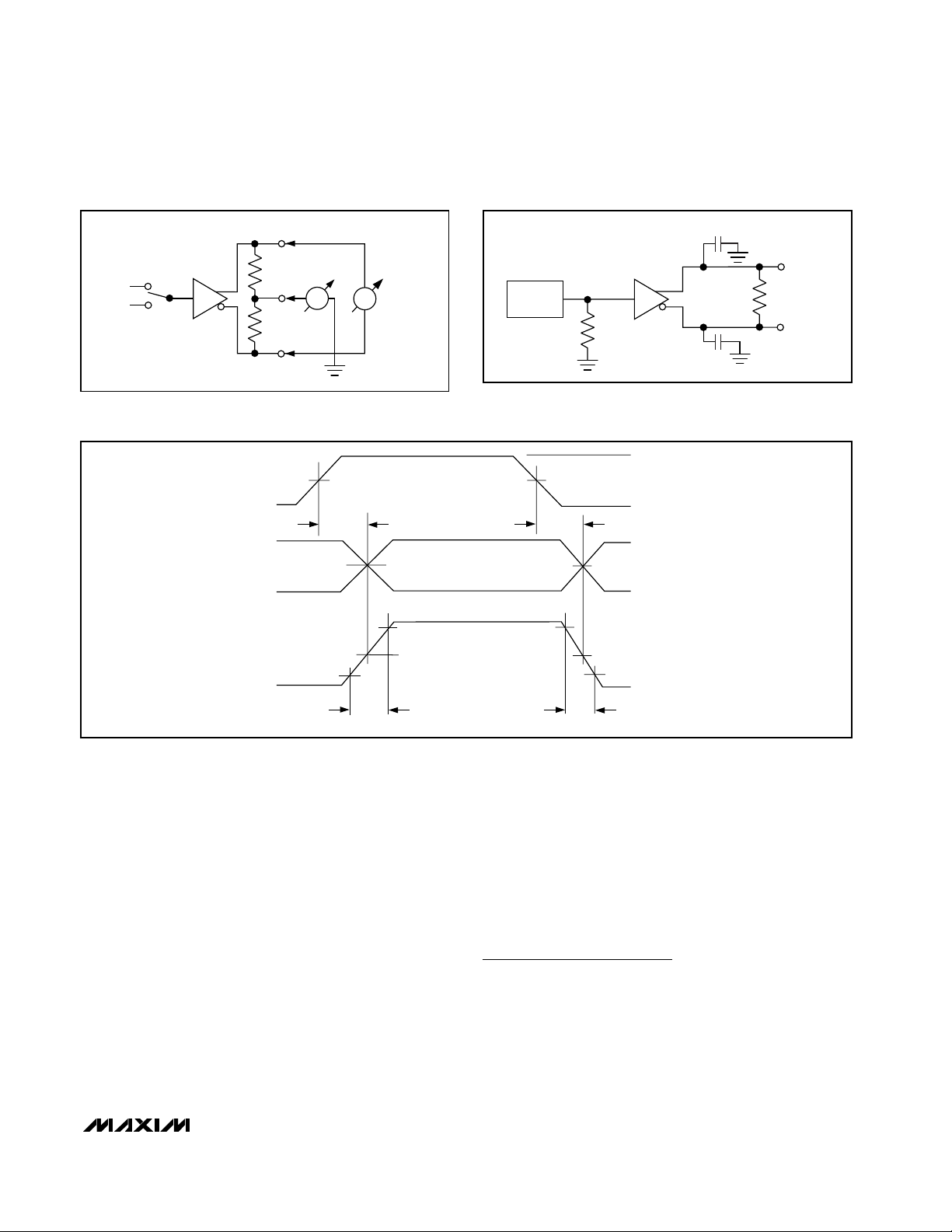
Figure 1. Driver VODand VOSTest Circuit
Figure 2. Driver Propagation Delay and Transition Time Test
Circuit
Figure 3. Driver Propagation Delay and Transition Time Waveforms
OUT_+
V
GND
CC
IN_
RL/2
R
/2
L
V
OUT_-
IN_
-
OUT_
OUT_+
V
DIFF
OS
20%
1.5V
t
PLHD
OS
V
V
OD
0 DIFFERENTIAL
80%
V
0
DIFF
C
L
50Ω
IN_
C
L
GENERATOR
3V
1.5V
0
t
PHLD
V
OH
0
V
OL
80%
= (V
+) - (V
OUT_
-)
0
20%
OUT_
R
OUT_ +
L
OUT_ -
t
TLH
t
THL
Page 8
MAX9123
Quad LVDS Line Driver with
Flow-Through Pinout
8 _______________________________________________________________________________________
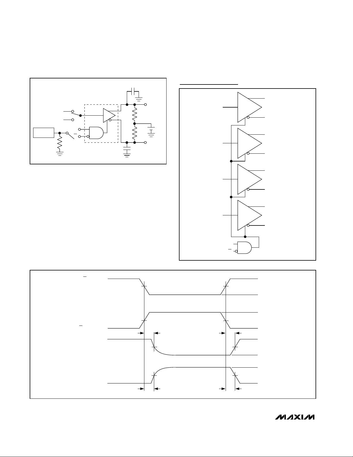
Figure 5. Driver High-Impedance Delay Waveform
Figure 4. Driver High-Impedance Delay Test Circuit
Functional Diagram
C
L
OUT_+
V
CC
GND
GENERATOR
EN
EN
50
Ω
IN_
1/4 MAX9123
R
L/2
+1.2V
R
L/2
OUT_-
C
L
OUT1+
IN1
OUT1-
OUT2+
IN2
OUT2-
OUT3+
IN3
OUT3-
OUT4+
IN4
OUT4-
EN WHEN EN = 0 OR OPEN
EN WHEN EN = V
OUT_+ WHEN IN_ = V
OUT_- WHEN IN_ = 0
OUT_+ WHEN IN_ = 0
OUT_- WHEN IN_ = V
EN
EN
3V
1.5V
1.5V
CC
CC
CC
t
PHZ
t
PLZ
1.5V
1.5V
0
3V
t
PZH
50%50%
50%50%
t
PZL
0
V
1.2V
1.2V
V
OH
OL
Page 9

MAX9123
Quad LVDS Line Driver with
Flow-Through Pinout
_______________________________________________________________________________________ 9
Package Information
TSSOP,NO PADS.EPS
Page 10

MAX9123
Quad LVDS Line Driver with
Flow-Through Pinout
Maxim cannot assume responsibility for use of any circuitry other than circuitry entirely embodied in a Maxim product. No circuit patent licenses are
implied. Maxim reserves the right to change the circuitry and specifications without notice at any time.
10 ____________________Maxim Integrated Products, 120 San Gabriel Drive, Sunnyvale, CA 94086 408-737-7600
© 2001 Maxim Integrated Products Printed USA is a registered trademark of Maxim Integrated Products.
Package Information (continued)
SOICN.EPS
 Loading...