

Page 1
General Description
The MAX9121/MAX9122 quad low-voltage differential signaling (LVDS) differential line receivers are ideal for applications requiring high data rates, low power, and low
noise. The MAX9121/MAX9122 are guaranteed to receive
data at speeds up to 500Mbps (250MHz) over controlledimpedance media of approximately 100Ω. The transmission media may be printed circuit (PC) board traces or
cables.
The MAX9121/MAX9122 accept four LVDS differential
inputs and translate them to LVCMOS outputs. The
MAX9122 features integrated parallel termination resistors (nominally 107Ω), which eliminate the requirement
for four discrete termination resistors and reduce stub
lengths. The MAX9121 inputs are high impedance and
require an external termination resistor when used in a
point-to-point connection.
The devices support a wide common-mode input range of
0.05V to 2.35V, allowing for ground potential differences
and common-mode noise between the driver and the
receiver. A fail-safe feature sets the output high when the
inputs are open, or when the inputs are undriven and
shorted or parallel terminated. The EN and EN inputs control the high-impedance output. The enables are common
to all four receivers. Inputs conform to the ANSI TIA/EIA644 LVDS standard. Flow-through pinout simplifies PC
board layout and reduces crosstalk by separating the
LVDS inputs and LVCMOS outputs. The MAX9121/
MAX9122 operate from a single +3.3V supply, and are
specified for operation from -40°C to +85°C. These
devices are available in 16-pin TSSOP and SO packages.
Refer to the MAX9123 data sheet for a quad LVDS line driver with flow-through pinout.
Applications
Digital Copiers
Laser Printers
Cellular Phone Base Stations
Add/Drop Muxes
Digital Cross-Connects
DSLAMs
Network Switches/Routers
Backplane Interconnect
Clock Distribution
____________________________Features
♦ Integrated Termination Eliminates Four External
Resistors (MAX9122)
♦ Flow-Through Pinout
Simplifies PC Board Layout
Reduces Crosstalk
♦ Pin Compatible with DS90LV048A
♦ Guaranteed 500Mbps Data Rate
♦ 300ps Pulse Skew (max)
♦ Conform to ANSI TIA/EIA-644 LVDS Standard
♦ Single +3.3V Supply
♦ Fail-Safe Circuit
MAX9121/MAX9122
Quad LVDS Line Receivers with
Integrated Termination and Flow-Through Pinout
________________________________________________________________ Maxim Integrated Products 1
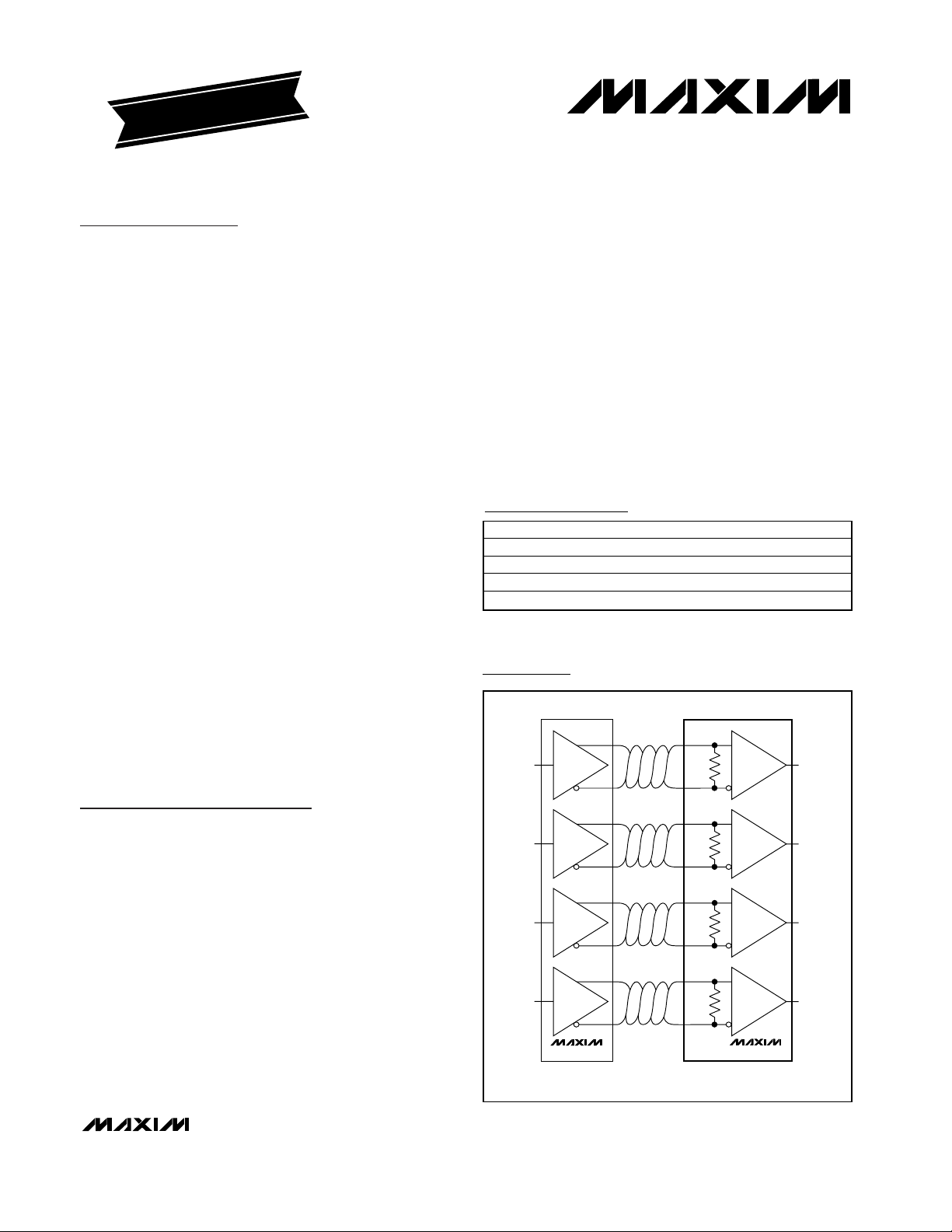
Typical Application Circuit
19-1909; Rev 0; 6/01
For pricing, delivery, and ordering information, please contact Maxim/Dallas Direct! at
1-888-629-4642, or visit Maxim’s website at www.maxim-ic.com.
EVALUATION KIT
AVAILABLE
Ordering Information
Pin Configuration appears at end of data sheet.
MAX9123
MAX9122
T
X
T
X
T
X
T
X
R
X
R
X
R
X
R
X
107Ω
107Ω
107Ω
107Ω
100Ω SHIELDED TWISTED CABLE OR MICROSTRIP PC BOARD TRACES
LVDS SIGNALS
LVTTL/LVCMOS
DATA OUTPUT
LVTTL/LVCMOS
DATA INPUT
PART TEMP. RANGE PIN-PACKAGE
MAX9121EUE -40°C to +85°C 16 TSSOP
MAX9121ESE -40°C to +85°C 16 SO
MAX9122EUE -40°C to +85°C 16 TSSOP
MAX9122ESE -40°C to +85°C 16 SO
Page 2
VCCto GND...........................................................-0.3V to +4.0V
IN_+, IN_- to GND .................................................-0.3V to +4.0V
EN, EN to GND...........................................-0.3V to (V
CC
+ 0.3V)
OUT_ to GND .............................................-0.3V to (V
CC
+ 0.3V)
Continuous Power Dissipation (T
A
= +70°C)
16-Pin TSSOP (derate 9.4mW/°C above +70°C) .........755mW
16-Pin SO (derate 8.7mW/°C above +70°C)................696mW
Storage Temperature Range .............................-65°C to +150°C
Maximum Junction Temperature .....................................+150°C
Operating Temperature Range ...........................-40°C to +85°C
Lead Temperature (soldering, 10s) .................................+300°C
ESD Protection
(Human Body Model, IN_+, IN_-) ....................................±8kV
MAX9121/MAX9122
Quad LVDS Line Receivers with
Integrated Termination and Flow-Through Pinout
2 _______________________________________________________________________________________
ABSOLUTE MAXIMUM RATINGS
DC ELECTRICAL CHARACTERISTICS
(VCC= +3.0V to +3.6V, differential input voltage |VID| = 0.1V to 1.0V, common-mode voltage VCM= |VID/2| to 2.4V - |VID/2|,
T
A
= -40°C to +85°C. Typical values are at VCC= +3.3V, TA= +25°C, unless otherwise noted.) (Note 1)
Stresses beyond those listed under “Absolute Maximum Ratings” may cause permanent damage to the device. These are stress ratings only, and functional
operation of the device at these or any other conditions beyond those indicated in the operational sections of the specifications is not implied. Exposure to
absolute maximum rating conditions for extended periods may affect device reliability.
LVDS INPUTS (IN_+, IN_-)
Differential Input High Threshold V
Differential Input Low Threshold V
Input Current (MAX9121) IIN_+, IIN_-
Power-Off Input Current
(MAX9121)
Input Resistor 1 R
Input Resistor 2 R
Differential Input Resistance
(MAX9122)
LVCMOS/LVTTL OUTPUTS (OUT_)
Output High Voltage (Table 1) V
Output Low Voltage V
Output Short-Circuit Current I
Output High-Impedance Current I
PARAMETER SYMBOL CONDITIONS MIN TYP MAX UNITS
TH
TL
0.1V ≤VID≤ 0.6V -20 20 µA
I
INOFF
R
DIFF
0.6V <V
0.1V ≤VID≤ 0.6V, VCC = 0 -20 20 µA
0.6V <VID≤ 1.0V, VCC = 0 -25 25 µA
V
IN1
IN2
CC
V
CC
V
CC
≤ 1.0V -25 25 µA
ID
= 3.6V or 0, Figure 1 35 kΩ
= 3.6V or 0, Figure 1 132 kΩ
= 3.6V or 0, Figure 1 90 107 132 Ω
IOH = -4.0mA
(MAX9121)
OH
IOH = -4.0mA
(MAX9122)
IOL = +4.0mA, VID = -100mV 0.1 0.25 V
OL
OS
OZ
Enabled, VID = 0.1V, V
Disabled, V
OUT
100 mV
-100 mV
Open, undriven short, or
undriven 100Ω parallel
2.7 3.2
termination
V
= +100mV 2.7 3.2
ID
Open or undriven short 2.7 3.2
= +100mV 2.7 3.2
V
ID
_ = 0 (Note 2) -15 -120 mA
OUT
= 0 or V
CC
-10 +10 µA
V
Page 3
MAX9121/MAX9122
Quad LVDS Line Receivers with
Integrated Termination and Flow-Through Pinout
_______________________________________________________________________________________ 3
AC ELECTRICAL CHARACTERISTICS
(VCC= +3.0V to +3.6V, CL= 15pF, differential input voltage |VID| = 0.2V to 1.0V, common-mode voltage VCM= |VID/2| to 2.4V |V
ID
/2|, input rise and fall time = 1ns (20% to 80%), input frequency = 100MHz, TA= -40°C to +85°C. Typical values are at VCC=
+3.3V, V
CM
= 1.2V, |VID| = 0.2V, TA= +25°C, unless otherwise noted.) (Notes 3, 4)
DC ELECTRICAL CHARACTERISTICS (continued)
(VCC= +3.0V to +3.6V, differential input voltage |VID| = 0.1V to 1.0V, common-mode voltage VCM= |VID/2| to 2.4V - |VID/2|,
T
A
= -40°C to +85°C. Typical values are at VCC= +3.3V, TA= +25°C, unless otherwise noted.) (Note 1)
LOGIC INPUTS (EN, EN)
Input High Voltage V
Input Low Voltage V
Input Current I
SUPPLY
Supply Current I
Disabled Supply Current I
PARAMETER SYMBOL CONDITIONS MIN TYP MAX UNITS
IH
IL
IN
CC
CCZ
2.0 V
0 0.8 V
V
= VCC or 0 -15 15 µA
IN_
Enabled, inputs open 9 15 mA
Disabled, inputs open 0.07 0.5 mA
CC
V
Differential Propagation Delay
High to Low
Differential Propagation Delay
Low to High
Differential Pulse Skew [t
t
PLHD
Differential Channel-to-Channel
Skew (Note 6)
Differential Part-to-Part Skew
(Note 7)
Differential Part-to-Part Skew
(Note 8)
Rise-Time t
Fall-Time t
Disable Time High to Z t
Disable Time Low to Z t
Enable Time Z to High t
Enable Time Z to Low t
Maximum Operating Frequency
(Note 9)
PARAMETER SYMBOL CONDITIONS MIN TYP MAX UNITS
] (Note 5)
PHLD
t
PHLD
t
PLHD
t
SKD1
t
SKD2
t
SKD3
t
SKD4
TLH
THL
PHZ
PLZ
PZH
PZL
f
MAX
Figures 2 and 3 1.2 1.93 2.7 ns
Figures 2 and 3 1.2 1.79 2.7 ns
Figures 2 and 3 140 300 ps
Figures 2 and 3 400 ps
Figures 2 and 3 0.8 ns
Figures 2 and 3 1.5 ns
Figures 2 and 3 0.55 1.0 ns
Figures 2 and 3 0.54 1.0 ns
RL = 2kΩ, Figures 4 and 5 14 ns
RL = 2kΩ, Figures 4 and 5 14 ns
RL = 2kΩ, Figures 4 and 5 70 ns
RL = 2kΩ, Figures 4 and 5 70 ns
All channels switching 250 300 MHz
Page 4
MAX9121/MAX9122
Quad LVDS Line Receivers with
Integrated Termination and Flow-Through Pinout
4 _______________________________________________________________________________________
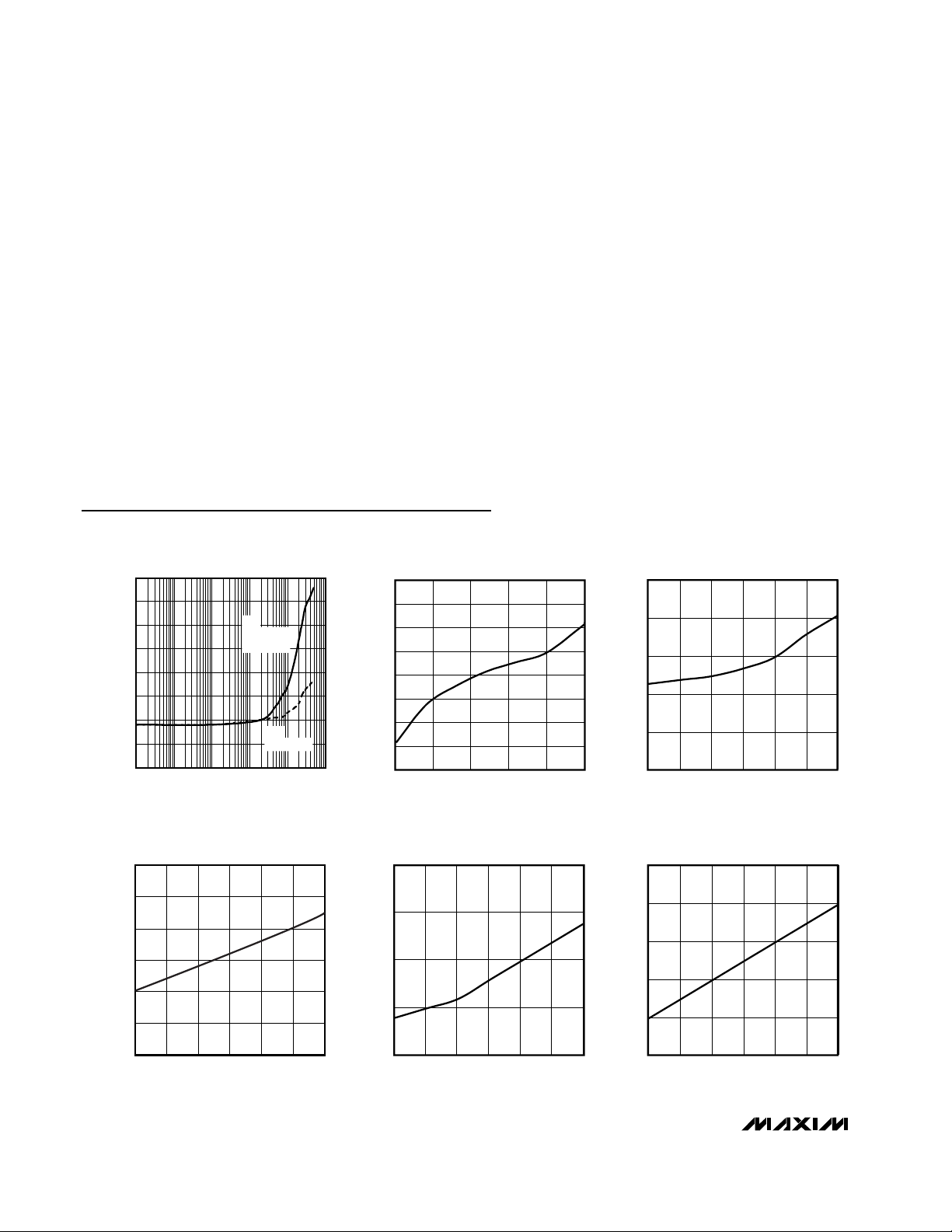
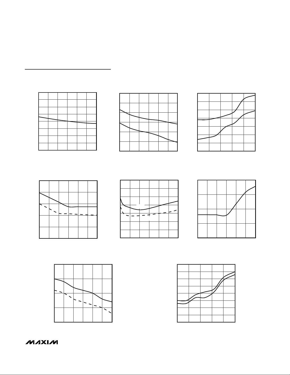
Typical Operating Characteristics
(VCC= +3.3V, VCM= +1.2V, |VID| = 0.2V, CL= 15pF, TA = +25°C, unless otherwise noted.) (Figures 2 and 3)
40
0
0.01 0.1 1000100
SUPPLY CURRENT
vs. FREQUENCY
10
20
30
MAX9121/22 toc01
FREQUENCY (MHz)
SUPPLY CURRENT (mA)
110
ALL
CHANNELS
SWITCHING
ONE
SWITCHING
7.00
7.50
8.00
8.50
9.00
9.50
10.00
10.50
11.00
-40 -15 10 35 60 85
SUPPLY CURRENT vs.
TEMPERATURE
MAX9121/22 toc02
TEMPERATURE (°C)
SUPPLY CURRENT (mA)
0
10
30
20
40
50
3.0 3.3 3.6
DIFFERENTIAL THRESHOLD VOLTAGE
vs. SUPPLY VOLTAGE
MAX9121/22 toc03
SUPPLY VOLTAGE (V)
DIFFERENTIAL THRESHOLD VOLTAGE (mV)
Note 1: Current into a pin is defined as positive. Current out of a pin is defined as negative. All voltages are referenced to ground
except V
TH
, VTL, and VID.
Note 2: Short only one output at a time. Do not exceed the absolute maximum junction temperature specification.
Note 3: AC parameters are guaranteed by design and characterization.
Note 4: C
L
includes scope probe and test jig capacitance.
Note 5: t
SKD1
is the magnitude difference of differential propagation delays in a channel. t
SKD1
= |t
PHLD
- t
PLHD
|.
Note 6: t
SKD2
is the magnitude difference of the t
PLHD
or t
PHLD
of one channel and the t
PLHD
or t
PHLD
of any other channel on the same part.
Note 7: t
SKD3
is the magnitude difference of any differential propagation delays between parts operating over rated conditions at
the same V
CC
and within 5°C of each other.
Note 8: t
SKD4
is the magnitude difference of any differential propagation delays between parts operating over rated conditions.
Note 9: f
MAX
generator output conditions: rise-time = fall-time = 1ns (0% to 100%), 50% duty cycle, VOH= +1.3V, VOL= +1.1V,
MAX9121/MAX9122 output criteria: 60% to 40% duty cycle, V
OL
= 0.4V (max), VOH= 2.7V (min), load = 15pF.
3.0 3.3 3.6
OUTPUT SHORT-CIRCUIT CURRENT
vs. SUPPLY VOLTAGE
MAX9121/22 toc04
SUPPLY VOLTAGE (V)
OUTPUT SHORT-CIRCUIT CURRENT (mA)
-70
-75
-80
-65
-90
-95
-85
1.30
1.25
1.20
1.15
1.10
3.0 3.3 3.6
OUTPUT HIGH-IMPEDANCE CURRENT
vs. SUPPLY VOLTAGE
MAX9121/22 toc05
SUPPLY VOLTAGE (V)
OUTPUT HIGH-IMPEDANCE CURRENT (nA)
2.7
2.9
3.3
3.1
3.5
3.7
3.0 3.3 3.6
OUTPUT HIGH VOLTAGE vs.
SUPPLY VOLTAGE
MAX9121/22 toc06
SUPPLY VOLTAGE (V)
OUTPUT HIGH VOLTAGE (V)
AC ELECTRICAL CHARACTERISTICS (continued)
(VCC= +3.0V to +3.6V, CL= 15pF, differential input voltage |VID| = 0.2V to 1.0V, common-mode voltage VCM= |VID/2| to 2.4V |V
ID
/2|, input rise and fall time = 1ns (20% to 80%), input frequency = 100MHz, TA= -40°C to +85°C. Typical values are at VCC=
+3.3V, V
CM
= 1.2V, |VID| = 0.2V, TA= +25°C, unless otherwise noted.) (Notes 3, 4)
Page 5
MAX9121/MAX9122
Quad LVDS Line Receivers with
Integrated Termination and Flow-Through Pinout
_______________________________________________________________________________________ 5
Typical Operating Characteristics (continued)
(VCC= +3.3V, VCM= +1.2V, |VID| = 0.2V, CL= 15pF, TA = +25°C, unless otherwise noted.) (Figures 2 and 3)
600
575
550
525
500
3.0 3.3 3.6
TRANSITION TIME vs.
SUPPLY VOLTAGE
MAX9121/22 toc13
SUPPLY VOLTAGE (V)
TRANSITION TIME (ps)
t
TLH
t
THL
450
475
500
525
550
575
600
625
650
-40 -15 10 35 60 85
TRANSITION TIME vs.
TEMPERATURE
MAX9121/22 toc14
TEMPERATURE (°C)
TRANSITION TIME (ps)
t
TLH
t
THL
3.0 3.3 3.6
OUTPUT LOW VOLTAGE
vs. SUPPLY VOLTAGE
MAX9121/22 toc07
SUPPLY VOLTAGE (V)
OUTPUT LOW VOLTAGE (mV)
93
94
95
96
97
92
99
100
98
1.60
1.80
1.70
2.00
1.90
2.10
2.20
3.0 3.3 3.6
DIFFERENTIAL PROPAGATION DELAY
vs. SUPPLY VOLTAGE
MAX9121/22 toc08
SUPPLY VOLTAGE (V)
DIFFERENTIAL PROPAGATION DELAY (ns)
t
PHLD
t
PLHD
1.50
1.70
1.90
2.10
-40 10-15 35 60 85
DIFFERENTIAL PROPAGATION DELAY
vs. TEMPERATURE
MAX9121/22 toc09
TEMPERATURE (°C)
DIFFERENTIAL PROPAGATION DELAY (ns)
t
PHLD
t
PLHD
1.25
1.50
2.00
1.75
2.25
2.50
-0.5 0.50 1.0 1.5 2.0 2.5
DIFFERENTIAL PROPAGATION DELAY
vs. COMMON-MODE VOLTAGE
MAX9121/22 toc10
COMMON-MODE VOLTAGE (V)
DIFFERENTIAL PROPAGATION DELAY (ns)
t
PHLD
t
PLHD
1.5
1.7
1.6
1.9
1.8
2.1
2.0
2.2
100 900 1700 2500
DIFFERENTIAL PROPAGATION DELAY
vs. DIFFERENTIAL INPUT VOLTAGE
MAX9121/22 toc11
DIFFERENTIAL INPUT VOLTAGE (mV)
DIFFERENTIAL PROPAGATION DELAY (ns)
t
PHLD
t
PLHD
200
175
150
125
100
3.0 3.3 3.6
DIFFERENTIAL PULSE SKEW vs.
SUPPLY VOLTAGE
MAX9121/22 toc12
SUPPLY VOLTAGE (V)
DIFFERENTIAL PULSE SKEW (ps)
Page 6

MAX9121/MAX9122
Quad LVDS Line Receivers with
Integrated Termination and Flow-Through Pinout
6 _______________________________________________________________________________________
Detailed Description
The LVDS interface standard is a signaling method
intended for point-to-point communication over a controlled-impedance medium as defined by the ANSI
TIA/EIA-644 and IEEE 1596.3 standards. The LVDS standard uses a lower voltage swing than other common
communication standards, achieving higher data rates
with reduced power consumption while reducing EMI
emissions and system susceptibility to noise.
The MAX9121/MAX9122 are 500Mbps, four-channel
LVDS receivers intended for high-speed, point-to-point,
low-power applications. Each channel accepts an
LVDS input and translates it to an LVTTL/LVCMOS output. The receiver is capable of detecting differential
signals as low as 100mV and as high as 1V within an
input voltage range of 0 to 2.4V. The 250mV to 400mV
differential output of an LVDS driver is nominally centered around a +1.2V offset. This offset, coupled with
the receiver’s 0 to 2.4V input voltage range, allows an
approximate ±1V shift in the signal (as seen by the
receiver). This allows for a difference in ground refer-
ences of the transmitter and the receiver, the commonmode effects of coupled noise, or both. The LVDS standards specify an input voltage range of 0 to +2.4V
referenced to receiver ground.
The MAX9122 has an integrated termination resistor
that is internally connected across each receiver input.
The internal termination saves board space, eases layout, and reduces stub length compared to an external
termination resistor. In other words, the transmission
line is terminated on the IC.
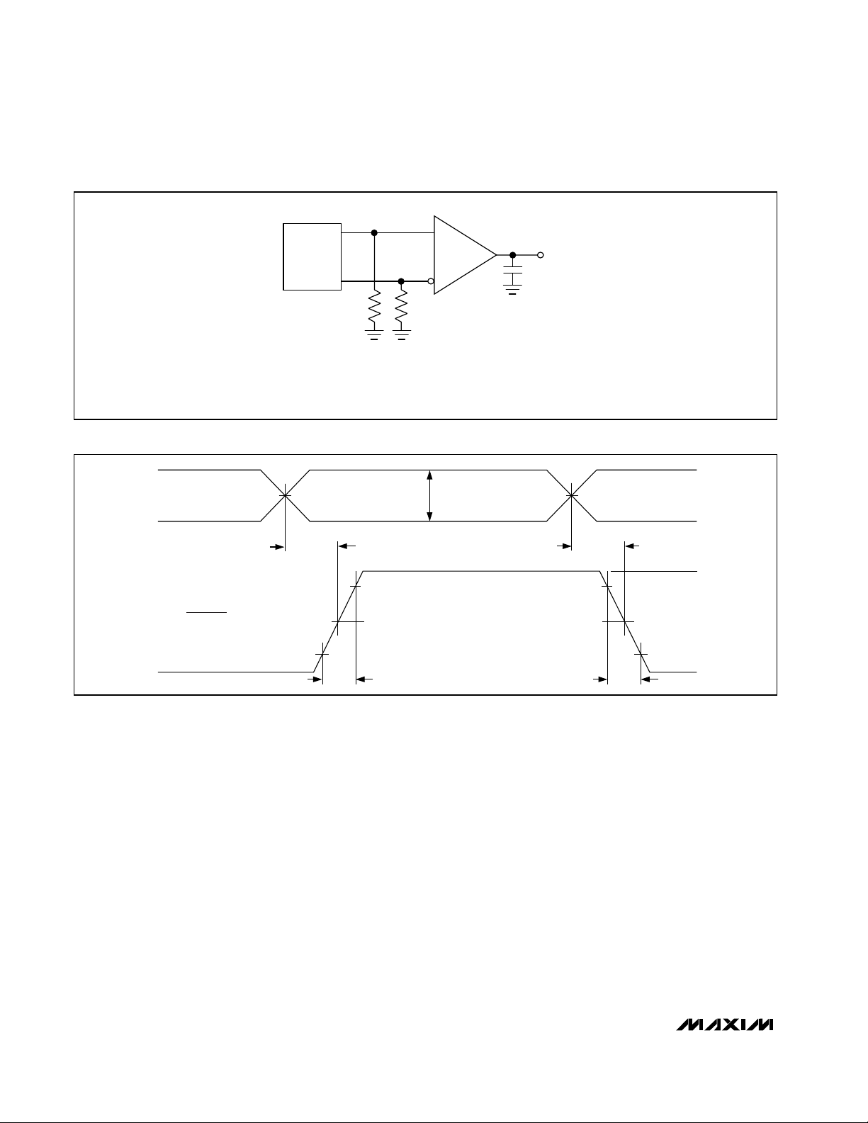
Fail-Safe
The fail-safe feature of the MAX9121/MAX9122 sets an
output high when:
• Inputs are open.
• Inputs are undriven and shorted.
• Inputs are undriven and terminated.
A fail-safe circuit is important because under these
conditions, noise at the inputs may switch the receiver
and it may appear to the system that data is being
Pin Description
Table 1. Input/Output Function Table
PIN NAME FUNCTION
1, 4, 5, 8 IN_- Inverting Differential Receiver Inputs
2, 3, 6, 7 IN_+ Noninverting Differential Receiver Inputs
9, 16 EN, EN
10, 11, 14, 15 OUT_ LVCMOS/LVTTL Receiver Outputs
12 GND Ground
13 V
All other combinations of ENABLE pins Don’t care Z
ENABLES INPUTS OUTPUT
EN EN (IN_+) - (IN_-) OUT_
H L or open
CC
Receiver Enable Inputs. When EN = high and EN = low or open, the outputs are active. For
other combinations of EN and EN, the outputs are disabled and in high impedance.
Power-Supply Input. Bypass VCC to GND with 0.1µF and 0.001µF ceramic capacitors.
V
≥ +100mV H
ID
VID ≤ -100mV L
MAX9121
MAX9122 Open or undriven short
Open, undriven short, or undriven
100Ω parallel termination
H
Page 7

received. Open or undriven terminated input conditions
can occur when a cable is disconnected or cut, or
when the LVDS driver outputs are high impedance. A
short condition can occur because of a cable failure.
The fail-safe input network (Figure 1) samples the input
common-mode voltage and compares it to VCC- 0.3V
(nominal). When the input is driven to levels specified in
the LVDS standards, the input to the common-mode
voltage is less than VCC- 0.3V and the fail-safe circuit
is not activated. If the inputs are open or if the inputs
are undriven and shorted or undriven and parallel terminated, there is no input current. In this case, a pullup
resistor in the fail-safe circuit pulls both inputs above
VCC- 0.3V, activating the fail-safe circuit and forcing
the output high.
Applications Information
Power-Supply Bypassing
Bypass the VCCpin with high-frequency surface-mount
ceramic 0.1µF and 0.001µF capacitors in parallel as
close to the device as possible, with the smaller valued
capacitor closest to V
CC
.
Differential Traces
Input trace characteristics affect the performance of the
MAX9121/MAX9122. Use controlled-impedance PC
board traces to match the cable characteristic impedance. The termination resistor is also matched to this
characteristic impedance.
Eliminate reflections and ensure that noise couples as
common mode by running the differential traces close
together. Reduce skew by matching the electrical
length of the traces. Excessive skew can result in a
degradation of magnetic field cancellation.
Each channel’s differential signals should be routed
close to each other to cancel their external magnetic
field. Maintain a constant distance between the differential traces to avoid discontinuities in differential
impedance. Avoid 90° turns and minimize the number
of vias to further prevent impedance discontinuities.
MAX9121/MAX9122
Quad LVDS Line Receivers with
Integrated Termination and Flow-Through Pinout
_______________________________________________________________________________________ 7
Figure 1. Input with Fail-Safe Network
V
CC
R
IN2
- 0.3V
V
CC
IN_+
R
IN1
R
IN1
IN_-
MAX9121 MAX9122
OUT_
IN_+
IN_-
V
CC
R
IN2
- 0.3V
V
CC
R
IN1
R
DIFF
R
IN1
OUT_
Page 8
MAX9121/MAX9122
Quad LVDS Line Receivers with
Integrated Termination and Flow-Through Pinout
8 _______________________________________________________________________________________
Cables and Connectors
Transmission media typically have a controlled differential impedance of 100Ω. Use cables and connectors
that have matched differential impedance to minimize
impedance discontinuities.
Avoid the use of unbalanced cables such as ribbon or
simple coaxial cable. Balanced cables such as twisted
pair offer superior signal quality and tend to generate
less EMI due to magnetic field canceling effects.
Balanced cables pick up noise as common mode,
which is rejected by the LVDS receiver.
Termination
The MAX9122 has an integrated termination resistor
connected across the inputs of each receiver. The
value of the integrated resistor is specified in the DC
characteristics.
The MAX9121 requires an external termination resistor.
The termination resistor should match the differential
impedance of the transmission line. Termination resistance values may range between 90Ω to 132Ω,
depending on the characteristic impedance of the
transmission medium.
When using the MAX9121, minimize the distance
between the input termination resistors and the
MAX9121 receiver inputs. Use 1% surface-mount resistors.
Figure 2. Propagation Delay and Transition Time Test Circuit
Figure 3. Propagation Delay and Transition Time Waveforms
IN_+
PULSE
GENERATOR**
IN_-
OUT_
C
L
50Ω REQUIRED FOR PULSE GENERATOR.
*
WHEN TESTING THE MAX9122, ADJUST THE
**
PULSE GENERATOR OUTPUT TO ACCOUNT
FOR INTERNAL TERMINATION RESISTOR.
IN_-
IN_+
VID = (V
) - (V
)
IN_+
NOTE: VCM = (V
2
OUT_
IN_-
+ V
)
IN-
IN+
VID = 0
t
PLHD
t
50Ω*50Ω*
80% 80%
50%
TLH
RECEIVER ENABLED
1/4 MAX9121/MAX9122
V
ID
VID = 0
t
PHLD
V
OH
50%
20%20%
V
t
THL
OL
Page 9

Board Layout
Because the MAX9121/MAX9122 feature a flow-through
pinout, no special layout precautions are required.
Keep the LVDS and any other digital signals separated
from each other to reduce crosstalk.
For LVDS applications, a four-layer PC board that provides separate power, ground, LVDS signals, and input
signals is recommended. Isolate the input LVDS signals
from each other to prevent coupling. Isolate the output
LVCMOS/LVTTL signals from each other to prevent
coupling. Separate the input LVDS signals from the output signals planes with the power and ground planes
for best results.
MAX9121/MAX9122
Quad LVDS Line Receivers with
Integrated Termination and Flow-Through Pinout
_______________________________________________________________________________________ 9
Figure 4. High-Impedance Delay Test Circuit
Figure 5. High-Impedance Delay Waveforms
Chip Information
TRANSISTOR COUNT: 1354
PROCESS: CMOS
V
CC
S
1
R
L
OUT_
C
L
3V
0
3V
t
PZL
50%
t
PZH
50%
0
V
V
V
GND
CC
OL
OH
GENERATOR
C
INCLUDES LOAD AND TEST JIG CAPACITANCE.
L
= VCC FOR t
S
1
= GND FOR t
S
1
EN WHEN EN = GND OR OPEN
EN WHEN EN = V
OUTPUT WHEN
= -100mV
V
ID
OUTPUT WHEN
= +100mV
V
ID
CC
1.5V
1.5V
IN_+
DEVICE
UNDER
EN
EN
50Ω
1/4 MAX9121/MAX9122
AND t
PZH
AND t
0.5V
PLZ
PHZ
0.5V
MEASUREMENTS.
MEASUREMENTS.
PZL
t
PLZ
t
PHZ
IN_-
TEST
1.5V
1.5V
Page 10
MAX9121/MAX9122
Quad LVDS Line Receivers with
Integrated Termination and Flow-Through Pinout
10 ______________________________________________________________________________________
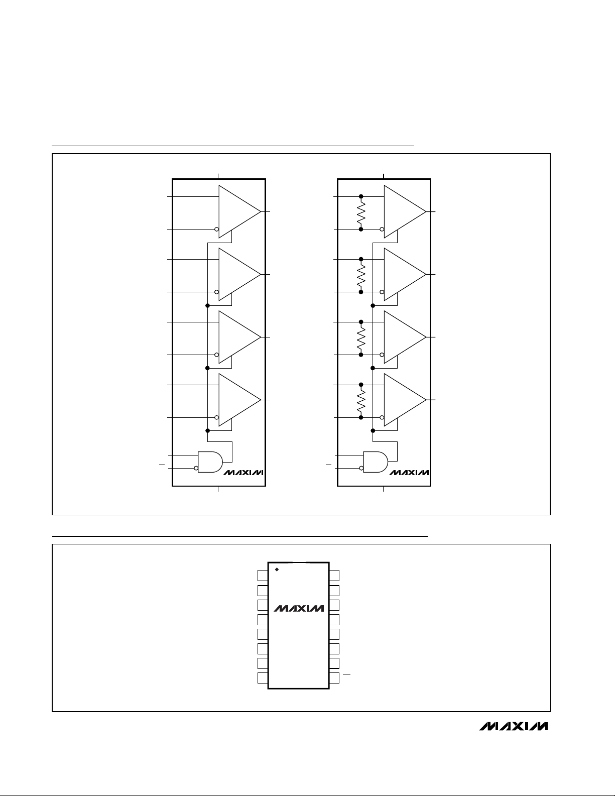
Functional Diagram
Pin Configuration
16
15
14
13
12
11
10
9
1
2
3
4
5
6
7
8
IN1- EN
OUT1
OUT2
V
CC
GND
OUT3
OUT4
EN
TOP VIEW
MAX9121
MAX9122
TSSOP/SO
IN1+
IN2+
IN3+
IN2-
IN3-
IN4+
IN4-
V
CC
V
CC
IN1+
IN1-
IN2+
IN2-
IN3+
IN3-
IN4+
IN4-
EN
EN
MAX9121 MAX9122
GND
OUT1
OUT2
OUT3
OUT4
IN1+
IN1-
IN2+
IN2-
IN3+
IN3-
IN4+
IN4-
107Ω
107Ω
107Ω
107Ω
EN
EN
GND
OUT1
OUT2
OUT3
OUT4
Page 11

MAX9121/MAX9122
Quad LVDS Line Receivers with
Integrated Termination and Flow-Through Pinout
______________________________________________________________________________________ 11
Package Information
TSSOP,NO PADS.EPS
Page 12

MAX9121/MAX9122
Quad LVDS Line Receivers with
Integrated Termination and Flow-Through Pinout
Maxim cannot assume responsibility for use of any circuitry other than circuitry entirely embodied in a Maxim product. No circuit patent licenses are
implied. Maxim reserves the right to change the circuitry and specifications without notice at any time.
12 ____________________Maxim Integrated Products, 120 San Gabriel Drive, Sunnyvale, CA 94086 408-737-7600
© 2001 Maxim Integrated Products Printed USA is a registered trademark of Maxim Integrated Products.
Package Information (continued)
SOICN.EPS
 Loading...