Page 1

General Description
The MAX913 single and MAX912 dual, high-speed,
low-power comparators have differential inputs and
complementary TTL outputs. Fast propagation delay
(10ns, typ), extremely low supply current, and a wide
common-mode input range that includes the negative
rail make the MAX912/MAX913 ideal for low-power,
high-speed, single +5V (or ±5V) applications such as
V/F converters or switching regulators.
The MAX912/MAX913 outputs remain stable through
the linear region. This feature eliminates output instability common to high-speed comparators when driven
with a slow-moving input signal.
The MAX912/MAX913 can be powered from a single
+5V supply or a ±5V split supply. The MAX913 is an
improved plug-in replacement for the LT1016. It provides significantly wider input voltage range and equivalent speed at a fraction of the power. The MAX912
dual comparator has equal performance to the MAX913
and includes independent latch controls.
Applications
Zero-Crossing Detectors
Ethernet Line Receivers
Switching Regulators
High-Speed Sampling Circuits
High-Speed Triggers
Extended Range V/F Converters
Fast Pulse Width/Height Discriminators
Features
♦ Ultra Fast (10ns)
♦ Single +5V or Dual ±5V Supply Operation
♦ Input Range Extends Below Negative Supply
♦ Low Power: 6mA (+5V) Per Comparator
♦ No Minimum Input Signal Slew-Rate Requirement
♦ No Power-Supply Current Spiking
♦ Stable in the Linear Region
♦ Inputs Can Exceed Either Supply
♦ Low Offset Voltage: 0.8mV
♦ Now Available in a Small µMAX Package
MAX912/MAX913
Single/Dual, Ultra-Fast, Low-Power
Precision TTL Comparators
________________________________________________________________ Maxim Integrated Products 1
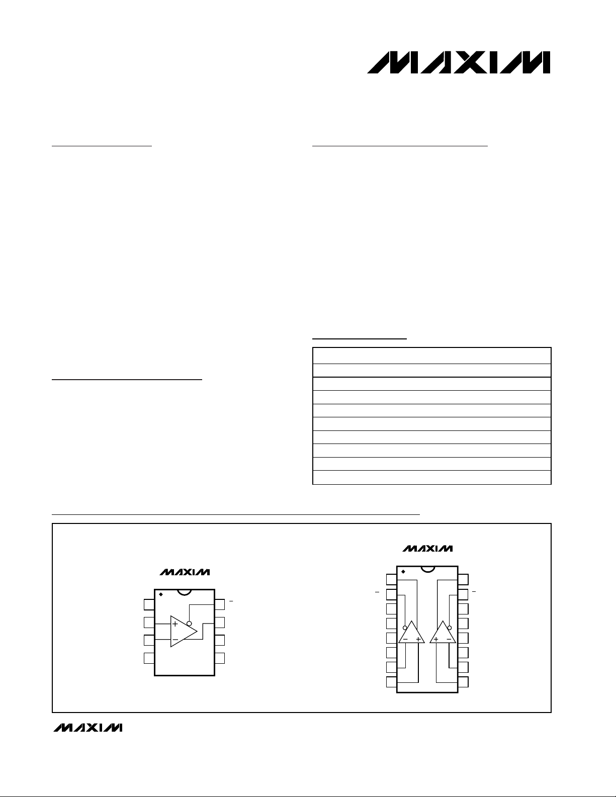
Pin Configurations
Ordering Information
19-0157; Rev 2; 8/03
For pricing, delivery, and ordering information, please contact Maxim/Dallas Direct! at
1-888-629-4642, or visit Maxim’s website at www.maxim-ic.com.
PART TEMP RANGE PIN-PACKAGE
MAX912CPE 0°C to +70°C 16 Plastic DIP
MAX912CSE 0°C to +70°C 16 Narrow SO
MAX912EPE -40°C to +85°C 16 Plastic DIP
MAX912ESE -40°C to +85°C 16 Narrow SO
MAX913CPA 0°C to +70°C 8 Plastic DIP
MAX913CSA 0°C to +70°C 8 SO
MAX913EPA -40°C to +85°C 8 Plastic DIP
MAX913ESA -40°C to +85°C 8 SO
MAX913EUA -40°C to +85°C 8 µMAX
TOP VIEW
MAX912
QA
MAX913
1
V+
2
3
IN-
4
DIP/SO/µMAX
87Q
6
5
QIN+
GND
LEV-
1
2
QA
GND
3
4
LEA
N.C.
5
6
V-
7
INA-
INA+
8
DIP/NARROW SO
A
B
QB
16
QB
15
GND
14
LEB
13
N.C.
12
V+
11
10
INB-
9
INB+
Page 2

MAX912/MAX913
Single/Dual, Ultra-Fast, Low-Power
Precision TTL Comparators
2 _______________________________________________________________________________________
ABSOLUTE MAXIMUM RATINGS
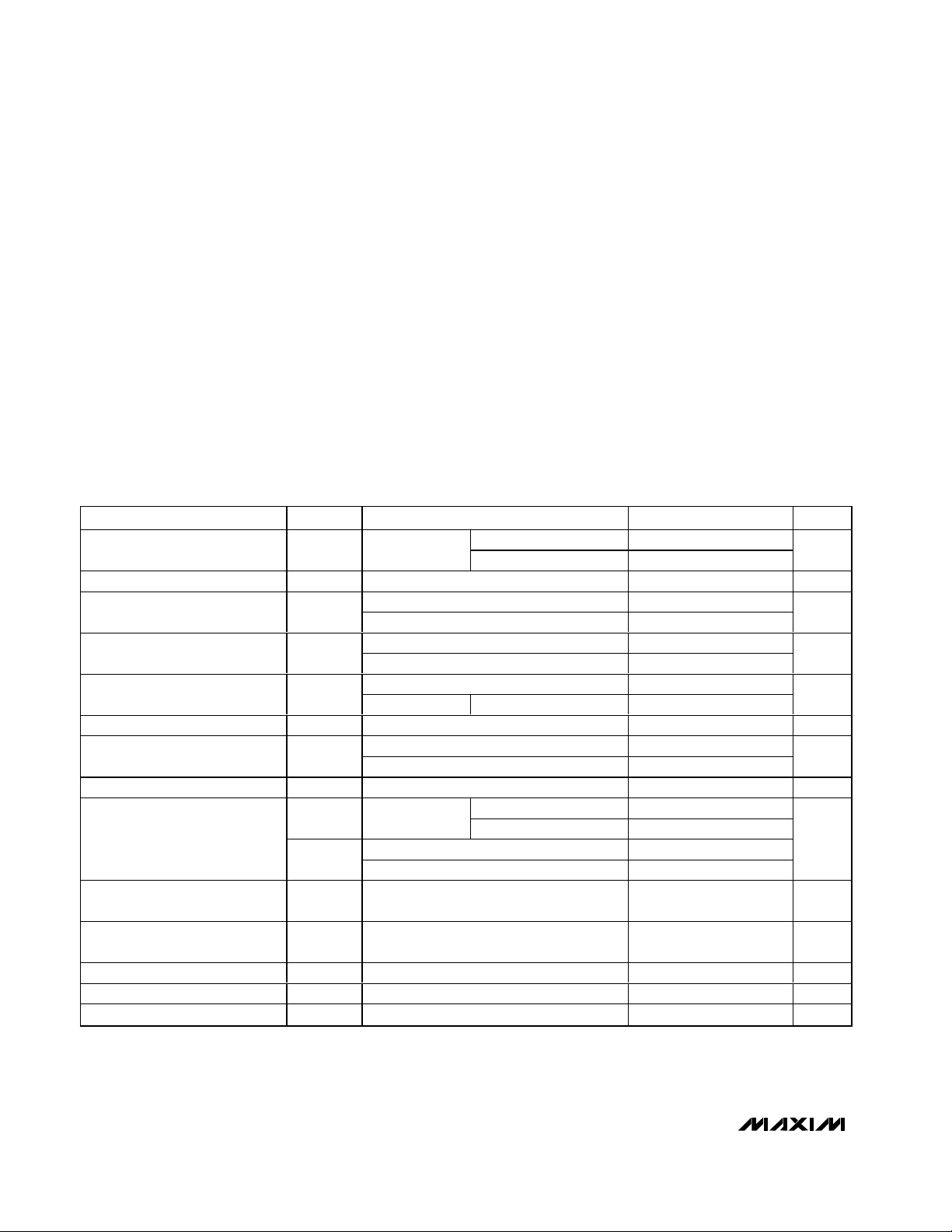
ELECTRICAL CHARACTERISTICS
V+ = +5V, V- = -5V, VQ= 1.4V, VLE= 0V, TA= T
MIN
to T
MAX
, unless otherwise noted. Typical values are at TA= +25°C.) (Note 1)
Stresses beyond those listed under “Absolute Maximum Ratings” may cause permanent damage to the device. These are stress ratings only, and functional
operation of the device at these or any other conditions beyond those indicated in the operational sections of the specifications is not implied. Exposure to
absolute maximum rating conditions for extended periods may affect device reliability.
Positive Supply Voltage .........................................................+7V
Negative Supply Voltage ........................................................-7V
V+ to V- ................................................................................+13V
Differential Input Voltage .....................................................+15V
Input Voltage (Referred to V-) ................................-0.3V to +14V
Latch Pin Voltage .............................................Equal to Supplies
Continuous Output Current...............................................±20mA
Continuous Power Dissipation (T
A
= +70°C)
8-Pin Plastic DIP (derate 9.09mW/°C above +70°C) ...727mW
8-Pin SO (derate 5.88mW/°C above +70°C)................471mW
8-Pin µMAX (derate 4.5mW/°C above +70°C) .............362mW
16-Pin Plastic DIP (derate 10.53mW/°C above +70°C)842mW
16-Pin Narrow SO (derate 8.70mW/°C above +70°C) .696mW
Operating Temperature Ranges:
MAX91_C_ _ ...........................................................0°C to +70°C
MAX91_E_ _.........................................................-40°C to +85°C
Storage Temperature Range .............................-65°C to +150°C
Lead Temperature (soldering, 10s) .................................+300°C
Input Offset Voltage (Note 2) V
Offset Drift TCV
Input Offset Current (Note 2) I
Input Bias Current I
Input Voltage Range V
Common-Mode Rejection Ratio CMRR -5.0V ≤ VCM ≤ +3.5V 80 110 dB
Power-Supply Rejection Ratio PSRR
Small-Signal Voltage Gain A
Output Voltage
Positive Supply Current Per
Comparator (Note 3)
Negative Supply Current Per
Comparator (Note 3)
Latch-Pin High Input Voltage V
Latch-Pin Low Input Voltage V
Latch-Pin Current I
PARAMETER SYMBOL CONDITIONS MIN TYP MAX UNITS
RS ≤ 100Ω
OS
OS
OS
V
V
I+ C, E temperature ranges 6 10 mA
TA = +25°C 0.3 0.5
TA = T
TA = +25°C25
B
C, E temperature ranges 8
C, E temperature ranges -5.2 +3.5
CM
Single +5V C, E temperature ranges -0.2 +3.5
Positive supply; 4.5V ≤ V+ ≤ 5.5V 60 85
Negative supply; -2V ≥ V- ≥ -7V 80 100
1V ≤ VQ ≤ 2V, TA = +25°C 1500 3500 V/V
V
V+ ≥ 4.5V
OH
I
OL
I- 1 2 mA
IH
IL
IL
SINK
TA = +25°C, I
VLE = 0V -1 -20 µA
MIN TO TMAX
= 4mA 0.3 0.5
SINK
TA = +25°C 0.1 2
= T
T
A
MIN TO TMAX
2 µV/°C
I
= 1mA 2.7 3.4
OUT
= 10mA 2.4 3.0
I
OUT
= 10mA 0.4
2.0 V
3
1
0.8 V
mV
µA
µA
V
dB
V
Page 3

MAX912/MAX913
Single/Dual, Ultra-Fast, Low-Power
Precision TTL Comparators
_______________________________________________________________________________________ 3
Note 1: All specifications are 100% tested at TA= +25°C, unless otherwise noted. Specification limits over temperature (TA= T
MIN
to T
MAX
) are guaranteed by design.
Note 2: Input Offset Voltage (V
OS
) is defined as the average of the two input offset voltages, measured by forcing first one output,
then the other to 1.4V. Input Offset Current (I
OS
) is defined the same way.
Note 3: Supply currents are measured with V
Q
driven to both VOHand VOL(not 1.4V).
Note 4: Propagation Delay (t
PD
) and Differential Propagation Delay (∆tPD) cannot be measured in automatic handling equipment
with low input overdrive values. Characterization and correlation tests have shown that t
PD
and ∆tPDlimits can be guaranteed by design. Electrical Characteristic DC tests are performed to guarantee that all internal bias conditions are correct.
For low overdrive conditions, V
OS
is added to overdrive. Differential Propagation Delay is defined as ∆tPD= t
PD+
- t
PD-
.
Note 5: Input latch setup time (t
SU
) is the interval in which the input signal must be stable prior to asserting the latch signal. The hold
time (t
H
) is the interval after the latch is asserted in which the input signal must be stable. These parameters are guaranteed
by design.
Note 6: Latch Propagation Delay (t
LPD
) is the delay time for the output to respond when the latch-enable pin is deasserted (see
Timing Diagram).
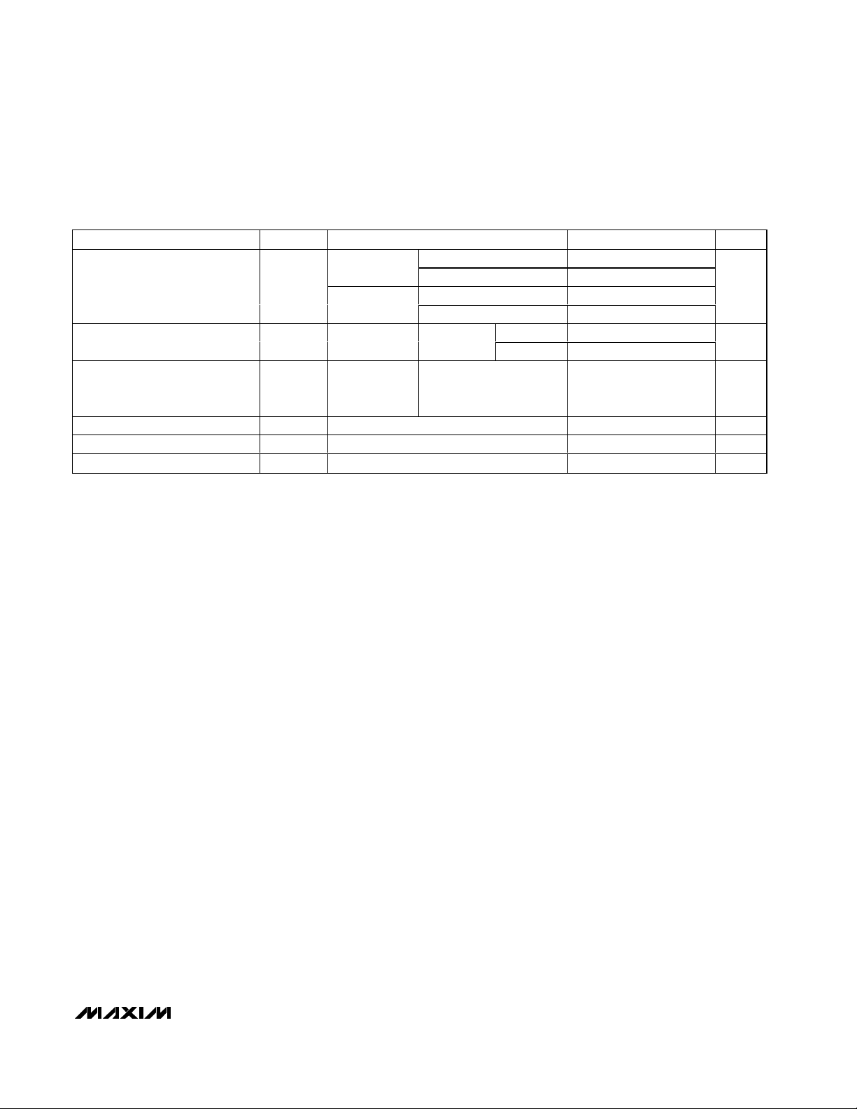
ELECTRICAL CHARACTERISTICS (continued)
V+ = +5V, V- = -5V, VQ= 1.4V, VLE= 0V, TA= T
MIN
to T
MAX
, unless otherwise noted. Typical values are at TA= +25°C.) (Note 1)
Propagation Delay (Note 4) t
Differential Propagation Delay
(Note 4)
Channel-to-Channel Propagation
Delay (Note 4)
Latch Setup Time (Note 5) t
Latch Hold Time (Note 5) t
Latch Propagation Delay (Note 6) t
PARAMETER SYMBOL CONDITIONS MIN TYP MAX UNITS
, t
PD+
PD-
∆t
PD
SU
H
LPD
∆VIN = 100mV,
V
OD
∆VIN = 100mV,
V
OD
∆VIN = 100mV,
V
OD
∆V
V
OD
(MAX912 only)
TA = +25°C1014
= 5mV
= 20mV
= 5mV
= 100mV,
IN
= 5mV
T
= T
A
MIN TO TMAX
TA = +25°C912
T
= T
A
MIN TO TMAX
T
= +25°C
A
T
= +25°C 500 ps
A
MAX913 2 4
MAX912 3 5
20 ns
52 ns
7ns
16
15
ns
ns
Page 4

MAX912/MAX913
Single/Dual, Ultra-Fast, Low-Power
Precision TTL Comparators
4 _______________________________________________________________________________________
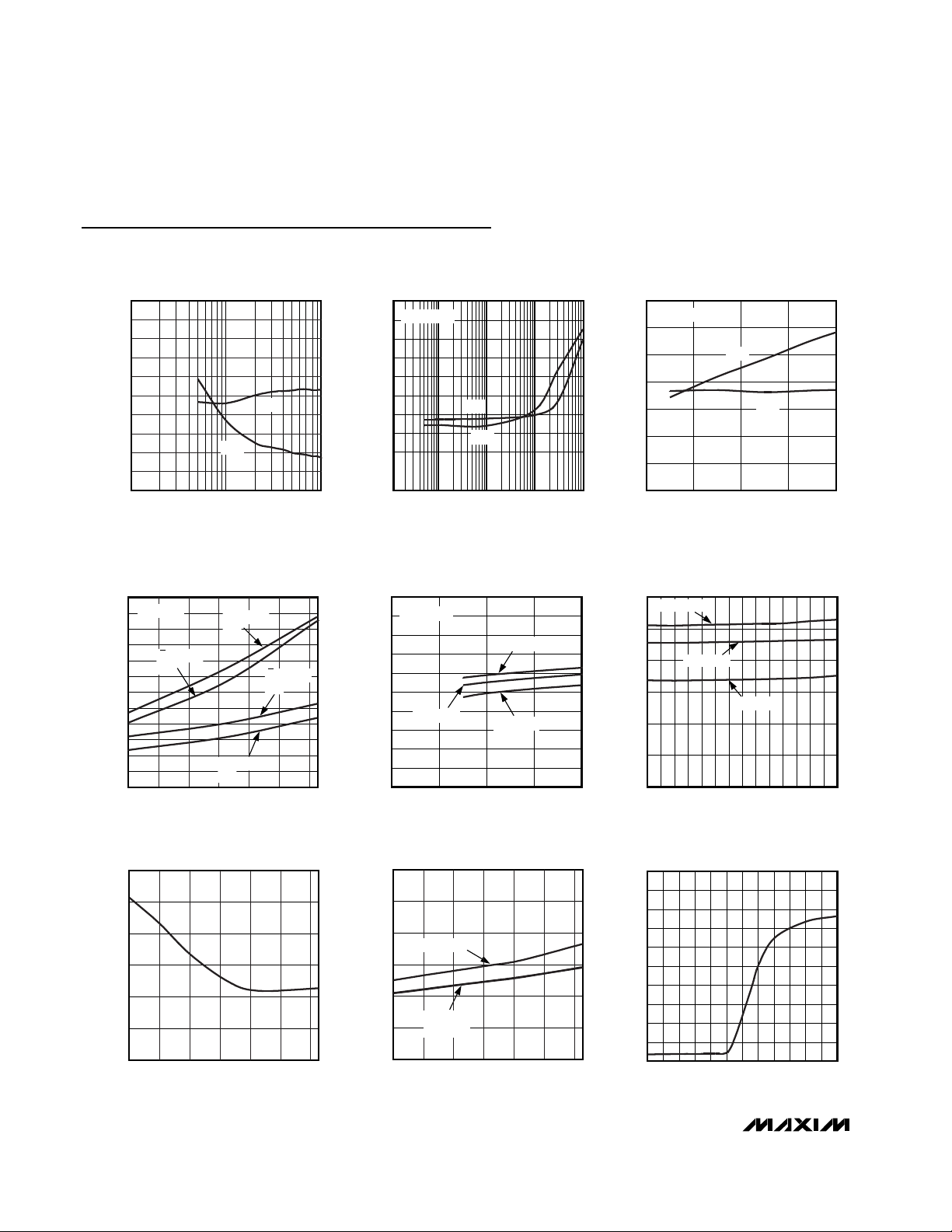
Typical Operating Characteristics
(V+ = +5V, V- = -5V, VLE= 0V, CL= 15pF, TA= +25°C, unless otherwise noted.)
10
9
8
7
6
5
1 10 100
PROPAGATION DELAY
vs. INPUT OVERDRIVE
MAX912/13 toc01
INPUT OVERDRIVE (mV)
PROPAGATION DELAY (ns)
t
PD+
t
PD-
20
0
1 10 100 1k 10k
PROPAGATION DELAY
vs. SOURCE RESISTANCE
4
MAX912/13 toc02
SOURCE RESISTANCE (Ω)
PROPAGATION DELAY (ns)
8
12
16
14
10
6
2
18
t
PD+
VOD = 10mV
t
PD-
PROPAGATION DELAY
vs. LOAD CAPACITANCE
MAX912/13 toc03
LOAD CAPACITANCE (pF)
PROPAGATION DELAY (ns)
403020
2
4
6
8
10
12
14
0
10 50
t
PD+
t
PD-
VOD = 10mV
PROPAGATION DELAY
vs. TEMPERATURE
MAX912/13 toc04
TEMPERATURE (°C)
PROPAGATION DELAY (ns)
60
40
200-20
6
7
8
9
10
11
5
-40
80
VOD = 5mV
Q OUTPUT
t
PD-
Q OUTPUT
t
PD-
Q OUTPUT
t
PD+
Q OUTPUT
t
PD+
POSITIVE SUPPLY CURRENT
(PER COMPARATOR)
vs. POSITIVE SUPPLY VOLTAGE
MAX912/13 toc05
V+ (V)
I+ (mA)
654
1
2
3
4
5
6
7
8
9
10
0
37
V- = 0 TO 5V
TA = +85°C
TA = -40°C
TA = +25°C
NEGATIVE SUPPLY CURRENT
(PER COMPARATOR)
vs. NEGATIVE SUPPLY VOLTAGE
MAX912/13 toc06
V- (V)
I- (mA)
654321
0.4
0.6
0.8
1.0
1.2
1.4
0.2
07
TA = +85°C
TA = -40°C
TA = +25°C
OFFSET VOLTAGE
vs. TEMPERATURE
MAX912/13 toc07
TEMPERATURE (°C)
OFFSET VOLTAGE (µV)
6040200-20
100
200
300
400
500
600
0
-40 80
INPUT BIAS CURRENT
vs. TEMPERATURE
MAX912/13 toc08
TEMPERATURE (°C)
INPUT BIAS CURRENT (µA)
6040200-20
0.5
1.0
1.5
2.0
2.5
3.0
0
-40 80
VCM = -5.2V
VCM = 0V
V
CM
= 3.5V
OUTPUT VOLTAGE
vs. DIFFERENTIAL INPUT VOLTAGE
MAX912/13 toc09
DIFFERENTIAL INPUT VOLTAGE (mV)
OUTPUT VOLTAGE (V)
21-2 -1 0
1
2
3
4
5
0
-3 3
Page 5

MAX912/MAX913
Single/Dual, Ultra-Fast, Low-Power
Precision TTL Comparators
_______________________________________________________________________________________ 5
Typical Operating Characteristics (continued)
(V+ = +5V, V- = -5V, VLE= 0V, CL= 15pF, TA= +25°C, unless otherwise noted.)
MAX912/MAX913 RESPONSE TO SLOW-MOVING TRIANGLE WAVE
POSITIVE-TO-NEGATIVE PROPAGATION DELAY
INPUT
100mV/div
OUTPUT
Q
1V/div
Q
5ns/div
MAX912/MAX913 RESPONSE TO
50MHZ (±10mV
) SINE WAVE
P-P
NEGATIVE-TO-POSITIVE PROPAGATION DELAY
5ns/div
INPUT
10mV/div
OUTPUT
Q
2V/div
INPUT
100mV/div
OUTPUT
Q
1V/div
Q
10ns/div
MAX912/MAX913 RESPONSE
20µs/div
INPUT
20mV/div
OUTPUT
Q
1V/div
Q
1V/div
INDUSTRY-STANDARD
686 RESPONSE
20µs/div
INPUT
20mV/div
OUTPUT
Q
1V/div
Q
1V/div
Page 6

MAX912/MAX913
Single/Dual, Ultra-Fast, Low-Power
Precision TTL Comparators
6 _______________________________________________________________________________________
MAX912 Pin Description
MAX913 Pin Description
PIN NAME FUNCTION
1 QA Comparator A TTL Output
2 QA Comparator A Complementary TTL Output
3, 14 GND Logic Ground. Connect both GND pins to ground.
4 LEA
5, 12 N.C. No Connection. Not internally connected.
6V-
7 INA- Comparator A Inverting Input
8 INA+ Comparator A Noninverting Input
9 INB+ Comparator B Noninverting Input
10 INB- Comparator B Inverting Input
11 V+ Positive Power Supply, +5V. Bypass to GND with a 0.1µF capacitor.
13 LEB
15 QB Comparator B Complementary TTL Output
16 QB Comparator B TTL Output
PIN NAME FUNCTION
1 V+ Positive Power Supply. Bypass to GND with a 0.1µF capacitor.
2 IN+ Noninverting Input
3 IN- Inverting Input
4V-
5LE
6 GND Logic Ground
7 Q TTL Output
8 Q Complementary TTL Output
Comparator A Latch Enable. QA and QA are latched when LEA is TTL high or floating. Comparator A
latch is transparent when LEA is low.
Negative Power Supply. -5V for dual supplies (bypass to GND with a 0.1µF capacitor) or GND for a
single supply.
Comparator B Latch Enable. QB and QB are latched when LEB is TTL high or floating. Comparator B
latch is transparent when LEB is low.
Negative Power Supply. -5V for dual supplies (bypass to GND with a 0.1µF capacitor) or GND for a
single supply.
Latch Enable. Q and Q are latched when LE is TTL high or floating. The comparator latch is
transparent when LE is low.
Page 7

MAX912/MAX913
Single/Dual, Ultra-Fast, Low-Power
Precision TTL Comparators
_______________________________________________________________________________________ 7
Detailed Description
The MAX912 (dual) and MAX913 (single) high-speed
comparators have a unique design that prevents oscillation when the comparator is in its linear region. No
minimum input slew rate is required.
Many high-speed comparators oscillate in the linear
region, as shown in the Typical Operating Characteris-
tics’ industry-standard 686 response graph. One way
to overcome this oscillation is to sample the output after
it has passed through the unstable region. Another
practical solution is to add hysteresis. Either solution
results in a loss of resolution and bandwidth.
Because the MAX912/MAX913 do not need hysteresis,
they offer high resolution to all signals—including lowfrequency signals.
The MAX912/MAX913 provide a TTL-compatible latch
function that holds the comparator output state (Figure 1).
As long as Latch Enable (LE) is high or floating, the input
signal has no effect on the output state. With LE low, the
outputs are controlled by the input differential voltage
and the latch is transparent.
Input Amplifier
A comparator can be thought of as having two sections; an input amplifier and a logic interface. The
MAX912/MAX913’s input amplifier is fully differential
with input offset voltage trimmed to below 2.0mV at
+25°C. Input common-mode range extends from
200mV below the negative supply rail to 1.5V below
the positive power supply. The total common-mode
range is 8.7V when operating from ±5VDC supplies.
The MAX912/MAX913’s amplifier has no built-in hysteresis. For highest accuracy, do not add hysteresis.
Figure 2 shows how hysteresis degrades resolution.
Resolution
A comparator’s ability to resolve small signal differences—its resolution—is affected by various factors.
As with most amplifiers, the most significant factors are
the input offset voltage (VOS) and the common-mode
and power-supply rejection ratios (CMRR, PSRR). If
source impedance is high, input offset current can be
significant. If source impedance is unbalanced, the
input bias current can introduce another error.
For high-speed comparators, an additional factor in
resolution is the comparator’s stability in its linear
region. Many high-speed comparators are useless in
their linear region because they oscillate. This makes
the differential input voltage region around 0V unusable, as does a high VOS. Hysteresis does not cure the
problem, but acts to keep the input away from its linear
range (Figure 2).
The MAX912/MAX913 do not oscillate in the linear
region, which greatly enhances the comparator’s resolution.
Figure 1. Timing Diagram
(DIFFERENTIAL)
ENABLE (LE)
V
LATCH
t
SU
IN
t
H
t
PD+
Q
∆t
PD
Q
t
PD-
t
LPD
Page 8

MAX912/MAX913
Applications Information
Power Supplies and Bypassing
The MAX912/MAX913 are tested with ±5V power supplies that provide an input common-mode range (VCM)
of 8.7V (-5.2V to +3.5V). Operation from a single +5V
supply provides a common-mode input range of 3.7V
(-0.2V to +3.5). Connect V- to GND for single-supply
operation. The MAX912/MAX913 will operate from a
minimum single-supply voltage of +4.5V.
The V+ supply provides power to both the analog input
stage and digital output circuits, whereas the V- supply
only powers the analog section. Bypass V+ and V- to
ground with 0.1µF to 1.0µF ceramic capacitors in parallel
with 10µF or greater tantalum capacitors. Connect the
ceramic capacitors very close to the MAX912/MAX913’s
supply pins, keeping leads short to minimize lead inductance. For particularly noisy applications, use ferrite
beads on the power-supply lines.
Board Layout
As with all high-speed components, careful attention to
layout is essential for best performance.
1) Use a printed circuit board with an unbroken ground
plane.
2) Pay close attention to the bandwidth of bypass components and keep leads short.
3) Avoid sockets; solder the comparator and other
components directly to the board to minimize
unwanted parasitic inductance and capacitance.
Input Slew Rate
The MAX912/MAX913 design eliminates the input slewrate requirement imposed on many standard comparators. As long as LE is high after the maximum propagation delay and the input is greater than the
comparator’s total DC error, the output will be valid
without oscillations.
Maximum Clock (LE) and Signal Rate
The maximum clock and signal rate is 70MHz, based
on the comparator’s rise and fall time with a 5mV overdrive at +25°C (Figure 1). With a 20mV overdrive, the
maximum propagation delay is 12ns and the clock signal rate is 85MHz.
Single/Dual, Ultra-Fast, Low-Power
Precision TTL Comparators
8 _______________________________________________________________________________________
Chip Information
MAX912 TRANSISTOR COUNT: 285
MAX913 TRANSISTOR COUNT: 154
PROCESS: Bipolar
Figure 2. Effect of Hysteresis on Input Resolution
IN+
IN-
Q
WITH HYSTERESIS
IDEAL (WITHOUT HYSTERESIS)
*WHEN HYSTERESIS IS ADDED, A COMPARATOR CANNOT RESOLVE ANY INPUT SIGNAL WITHIN THE HYSTERESIS BAND.
HYSTERESIS
BAND*
Page 9

MAX912/MAX913
Single/Dual, Ultra-Fast, Low-Power
Precision TTL Comparators
_______________________________________________________________________________________ 9
Package Information
(The package drawing(s) in this data sheet may not reflect the most current specifications. For the latest package outline information
go to www.maxim-ic.com/packages
.)
8
ÿ 0.50±0.1
0.6±0.1
0.6±0.1
1
D
TOP VIEW
A2
E H
A1
4X S
BOTTOM VIEW
A
8
1
DIM
A
A1
A2
b
c
D
e
E
H
L
α
S
INCHES
MIN
-
0.002
0.030
0.010
0.005
0.116
0.0256 BSC
0.116
0.188
0.016
0∞
0.0207 BSC
MAX
0.043
0.006
0.037
0.014
0.007
0.120
0.120
0.198
0.026
6∞
MILLIMETERS
MIN
0.05 0.15
0.25 0.36
0.13 0.18
2.95 3.05
2.95 3.05
4.78
0.41
MAX
- 1.10
0.950.75
0.65 BSC
5.03
0.66
0.5250 BSC
6∞0∞
8LUMAXD.EPS
e
FRONT VIEW
c
b
L
SIDE VIEW
α
PROPRIETARY INFORMATION
TITLE:
PACKAGE OUTLINE, 8L uMAX/uSOP
REV.DOCUMENT CONTROL NO.APPROVAL
21-0036
1
J
1
Page 10

MAX912/MAX913
Single/Dual, Ultra-Fast, Low-Power
Precision TTL Comparators
10 ______________________________________________________________________________________
Package Information (continued)
(The package drawing(s) in this data sheet may not reflect the most current specifications. For the latest package outline information
go to www.maxim-ic.com/packages
.)
N
1
e
TOP VIEW
D
B
A1
FRONT VIEW
INCHES
DIM
MIN
0.053A
0.004
A1
0.014
B
0.007
C
e 0.050 BSC 1.27 BSC
0.150
HE
A
C
L
E
H 0.2440.228 5.80 6.20
0.016L
VARIATIONS:
INCHES
MINDIM
D
0.189 0.197 AA5.004.80 8
0.337 0.344 AB8.758.55 14
D
0∞-8∞
MAX
0.069
0.010
0.019
0.010
0.157
0.050
MAX
0.3940.386D
MILLIMETERS
MAX
MIN
1.35
1.75
0.10
0.25
0.35
0.49
0.19
0.25
3.80 4.00
0.40 1.27
MILLIMETERS
MAX
MIN
9.80 10.00
N MS012
16
AC
SOICN .EPS
SIDE VIEW
PROPRIETARY INFORMATION
TITLE:
PACKAGE OUTLINE, .150" SOIC
REV.DOCUMENT CONTROL NO.APPROVAL
21-0041
1
B
1
Page 11

MAX912/MAX913
Single/Dual, Ultra-Fast, Low-Power
Precision TTL Comparators
Maxim cannot assume responsibility for use of any circuitry other than circuitry entirely embodied in a Maxim product. No circuit patent licenses are
implied. Maxim reserves the right to change the circuitry and specifications without notice at any time.
Maxim Integrated Products, 120 San Gabriel Drive, Sunnyvale, CA 94086 408-737-7600 ____________________ 11
© 2003 Maxim Integrated Products Printed USA is a registered trademark of Maxim Integrated Products.
Package Information (continued)
(The package drawing(s) in this data sheet may not reflect the most current specifications. For the latest package outline information
go to www.maxim-ic.com/packages
.)
PDIPN.EPS
 Loading...