

Page 1
General Description
The MAX9117–MAX9120 nanopower comparators in
space-saving SC70 packages feature Beyond-theRails™ inputs and are guaranteed to operate down to
+1.6V. The MAX9117/MAX9118 feature an on-board
1.252V ±1.75% reference and draw an ultra-low supply
current of only 600nA, while the MAX9119/MAX9120
(without reference) require just 350nA of supply current.
These features make the MAX9117–MAX9120 family of
comparators ideal for all 2-cell battery-monitoring/management applications.
The unique design of the output stage limits supply-current surges while switching, virtually eliminating the supply glitches typical of many other comparators. This
design also minimizes overall power consumption under
dynamic conditions. The MAX9117/MAX9119 have a
push-pull output stage that sinks and sources current.
Large internal-output drivers allow rail-to-rail output
swing with loads up to 5mA. The MAX9118/MAX9120
have an open-drain output stage that makes them suitable for mixed-voltage system design. All devices are
available in the ultra-small 5-pin SC70 package.
Applications
2-Cell Battery Monitoring/Management
Ultra-Low-Power Systems
Mobile Communications
Notebooks and PDAs
Threshold Detectors/Discriminators
Sensing at Ground or Supply Line
Telemetry and Remote Systems
Medical Instruments
Features
♦ Space-Saving SC70 Package (Half the Size of
SOT23)
♦ Ultra-Low Supply Current
350nA Per Comparator (MAX9119/MAX9120)
600nA Per Comparator with Reference
(MAX9117/MAX9118)
♦ Guaranteed to Operate Down to +1.6V
♦ Internal 1.252V ±1.75% Reference
(MAX9117/MAX9118)
♦ Input Voltage Range Extends 200mV
Beyond-the-Rails
♦ CMOS Push-Pull Output with ±5mA Drive
Capability (MAX9117/MAX9119)
♦ Open-Drain Output Versions Available
(MAX9118/MAX9120)
♦ Crowbar-Current-Free Switching
♦ Internal Hysteresis for Clean Switching
♦ No Phase Reversal for Overdriven Inputs
MAX9117–MAX9120
SC70, 1.6V, Nanopower, Beyond-the-Rails
Comparators With/Without Reference
________________________________________________________________ Maxim Integrated Products 1
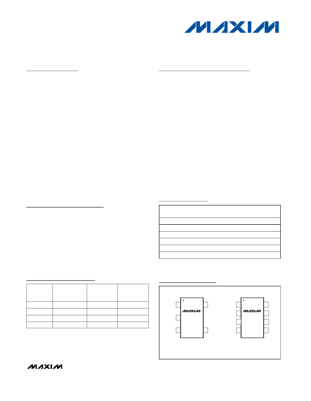
V
EE
IN- (REF)
IN+
1
5
V
CC
OUT
MAX9117
MAX9118
MAX9119
MAX9120
SC70
TOP VIEW
2
3
4
( ) ARE FOR MAX9117/MAX9118.
IN- (REF)
N.C.
V
EE
1
8
N.C.
N.C.
MAX9117
MAX9120
SO
2
IN+
3
V
CC
7
OUT
6
4
5
Typical Application Circuit appears at end of data sheet.
Pin Configurations
Selector Guide
Ordering Information
Beyond-the-Rails is a trademark of Maxim Integrated Products, Inc.
19-1862; Rev 4; 1/07
PART
INTERNAL
REFERENCE
OUTPUT
TYPE
SUPPLY
CURRENT
(nA)
MAX9117 Yes Push-Pull 600
MAX9118 Yes Open-Drain 600
350Push-PullNoMAX9119
MAX9120 No Open-Drain 350
For pricing, delivery, and ordering information, please contact Maxim/Dallas Direct! at
1-888-629-4642, or visit Maxim’s website at www.maxim-ic.com.
Note: All devices specified for over -40°C to +85°C operating
temperature range.
+Denotes lead-free package.
PART
MAX9117EXK-T 5 SC70-5
MAX9117ESA+ 8 SO
MAX9118EXK-T 5 SC70-5
MAX9119EXK-T 5 SC70-5
MAX9120EXK-T 5 SC70-5
MAX9120ESA+ 8 SO
PINPACKAGE
TOP
MARK
ABW
—
ABX
ABY
ABZ
—
PKG
CODE
X5-1
S8-2
X5-1
X5-1
X5-1
S8-2
Page 2
MAX9117–MAX9120
SC70, 1.6V, Nanopower, Beyond-the-Rails
Comparators With/Without Reference
2 _______________________________________________________________________________________
ABSOLUTE MAXIMUM RATINGS
ELECTRICAL CHARACTERISTICS—MAX9117/MAX9118 (with REF)
(VCC= +5V, VEE= 0V, V
IN+
= V
REF
, TA= -40°C to +85°C, unless otherwise noted. Typical values are at TA= +25°C.) (Note 1)
Stresses beyond those listed under “Absolute Maximum Ratings” may cause permanent damage to the device. These are stress ratings only, and functional
operation of the device at these or any other conditions beyond those indicated in the operational sections of the specifications is not implied. Exposure to
absolute maximum rating conditions for extended periods may affect device reliability.
Supply Voltage (VCCto VEE)..................................................+6V
Voltage Inputs (IN+, IN-, REF) .........(V
EE
- 0.3V) to (VCC+ 0.3V)
Output Voltage
MAX9117/MAX9119 ....................(V
EE
- 0.3V) to (VCC+ 0.3V)
MAX9118/MAX9120 ..................................(VEE- 0.3V) to +6V
Current Into Input Pins......................................................±20mA
Output Current..................................................................±50mA
Output Short-Circuit Duration .................................................10s
Continuous Power Dissipation (TA= +70°C)
5-Pin SC70 (derate 2.5mW/°C above +70°C).............200mW
8-Pin SO (derate 5.88mW/°C above +70°C)...............471mW
Operating Temperature Range ...........................-40°C to +85°C
Junction Temperature......................................................+150°C
Storage Temperature Range .............................-65°C to +150°C
Lead Temperature (soldering, 10s) .................................+300°C
PARAMETER
SYMBOL
CONDITIONS
MIN
TYP
MAX
UNITS
TA = +25°C 1.6 5.5
Supply Voltage Range V
CC
Inferred from the PSRR
test
T
A
= T
MIN
to T
MAX
1.8 5.5
V
VCC = 1.6V TA = +25°C
1
TA = +25°C
1.3
Supply Current I
CC
VCC = 5V
T
A
= T
MIN
to T
MAX
1.6
µA
IN+ Voltage Range V
IN+
Inferred from output swing test
V
EE
-
0.2
V
CC
+
0.2
V
TA = +25°C 1 5
Input Offset Voltage V
OS
(Note 2)
T
A
= T
MIN
to T
MAX
10
mV
Input-Referred Hysteresis V
HB
(Note 3) 4
mV
TA = +25°C
1
Input Bias Current I
B
TA = T
MIN
to T
MAX
2
nA
VCC = 1.6V to 5.5V, TA = +25°C 0.1 1
Power-Supply Rejection Ratio PSRR
V
CC
= 1.8V to 5.5V, TA = T
MIN
to T
MAX
1
mV/V
TA = +25°C
400
MAX9117, VCC = 5V,
I
SOURCE
= 5mA
T
A
= T
MIN
to T
MAX
500
200
Output Voltage Swing High
MAX9117,
I
SOURCE
= 1mA
V
CC
= 1.8V,
T
A
= T
MIN
to T
MAX
300
mV
TA = +25°C
400
VCC = 5V, I
SINK
= 5mA
T
A
= T
MIN
to T
MAX
500
200
Output Voltage Swing Low V
OL
I
SINK
= 1mA
V
CC
= 1.8V,
T
A
= T
MIN
to T
MAX
300
mV
Output Leakage Current I
LEAK
MAX9118 only, VO = 5.5V
1
µA
VCC = 5V 35
Sourcing, VO = V
EE
VCC = 1.6V 3
VCC = 5V 35
Output Short-Circuit Current I
SC
Sinking, VO = V
CC
VCC = 1.6V 3
mA
VCC = 1.6V 16
High-to-Low Propagation Delay
(Note 4)
t
PD-
V
CC
= 5V 14
µs
V
- V
CC
OH
VCC = 1.6V, TA = +25°C 100
VCC = 1.6V, TA = +25°C 100
0.60
0.68
0.15
190
190
0.002
Page 3
MAX9117–MAX9120
SC70, 1.6V, Nanopower, Beyond-the-Rails
Comparators With/Without Reference
_______________________________________________________________________________________ 3
ELECTRICAL CHARACTERISTICS—MAX9119/MAX9120 (without REF)
(VCC= +5V, VEE= 0V, VCM= 0V, TA= -40°C to +85°C, unless otherwise noted. Typical values are at TA= +25°C.) (Note 1)
ELECTRICAL CHARACTERISTICS—MAX9117/MAX9118 (with REF) (continued)
(VCC= +5V, VEE= 0V, V
IN+
= V
REF
, TA= -40°C to +85°C, unless otherwise noted. Typical values are at TA= +25°C.) (Note 1)
PARAMETER
SYMBOL
CONDITIONS
MIN
TYP
MAX
UNITS
VCC = 1.6V 15
MAX9117 only
V
CC
= 5V 40
VCC = 1.6V, R
PULLUP
= 100kΩ
16
Low-to-High Propagation Delay
(Note 4)
t
PD+
MAX9118 only
V
CC
= 5V,
R
PULLUP
= 100kΩ
45
µs
Rise Time t
RISE
MAX9117 only, CL = 15pF 1.6 µs
Fall Time t
FALL
CL = 15pF 0.2 µs
Power-Up Time t
ON
1.2
ms
TA = +25°C
Reference Voltage V
REF
TA = T
MIN
to T
MAX
V
Reference Voltage Temperature
Coefficient
pp m/
°C
BW = 10Hz to 100kHz 1.1
Reference Output Voltage Noise E
N
BW = 10Hz to 100kHz, C
REF
= 1nF 0.2
mV
RMS
Reference Line Regulation
∆V
CC
VCC = 1.6V to 5.5V
mV/V
Reference Load Regulation
∆I
OUT
∆I
OUT
= 10nA ±1
mV/
nA
1.230 1.252 1.274
1.196 1.308
TC
REF
∆V
/
REF
∆V
/
REF
100
0.25
Supply Voltage Range V
Supply Current I
Input Common-Mode
Voltage Range
Input Offset Voltage V
Input-Referred Hysteresis V
Input Bias Current I
Input Offset Current I
Power-Supply Rejection Ratio PSRR
Common-Mode Rejection Ratio CMRR (VEE - 0.2V) ≤ VCM ≤ (VCC + 0.2V) 0.5 3 mV/V
PARAMETER SYMBOL CONDITIONS MIN TYP MAX UNITS
CC
Inferred from the
PSRR test
TA = +25°C 1.6 5.5
T
= T
MIN
to T
MAX
A
1.8 5.5
VCC = 1.6V, TA = +25°C 0.35 0.80
CC
V
OS
VCC = 5V
Inferred from the CMRR test
CM
-0.2V ≤ VCM ≤
OS
CC
+ 0.2V)
(V
(Note 2)
-0.2V ≤ VCM ≤ (VCC + 0.2V) (Note 3) 4 mV
HB
TA = +25°C 0.15 1
B
TA = T
MIN
to T
MAX
VCC = 1.6V to 5.5V, TA = +25°C 0.1 1
VCC = 1.8V to 5.5V, TA = T
TA = +25°C 0.45 0.80
T
= T
MIN
to T
MAX
V
-
EE
A
0.2
TA = +25°C15
T
= T
MIN
to T
A
MAX
to T
MIN
MAX
V
µA
1.2
VCC +
0.2
V
mV
10
2
nA
75 pA
mV/V
1
Page 4
MAX9117–MAX9120
SC70, 1.6V, Nanopower, Beyond-the-Rails
Comparators With/Without Reference
4 _______________________________________________________________________________________
ELECTRICAL CHARACTERISTICS—MAX9119/MAX9120 (without REF) (continued)
(VCC= +5V, VEE= 0V, VCM= 0V, TA= -40°C to +85°C, unless otherwise noted. Typical values are at TA= +25°C.) (Note 1)
Note 1: All specifications are 100% tested at T
A
= +25°C. Specification limits over temperature (TA= T
MIN
to T
MAX
) are guaranteed
by design, not production tested.
Note 2: V
OS
is defined as the center of the hysteresis band at the input.
Note 3: The hysteresis-related trip points are defined as the edges of the hysteresis band, measured with respect to the center of
the band (i.e., V
OS
) (Figure 2).
Note 4: Specified with an input overdrive (V
OVERDRIVE
) of 100mV, and load capacitance of CL= 15pF. V
OVERDRIVE
is defined
above and beyond the offset voltage and hysteresis of the comparator input. For the MAX9117/MAX9118, reference voltage
error should also be added.
PARAMETER
SYMBOL
CONDITIONS
MIN
TYP
MAX
UNITS
TA = +25°C
MAX9119 only, VCC =
5V, I
SOURCE
= 5mA
T
A
= T
MIN
to T
MAX
VCC = 1.6V,
T
A
= +25°C
Output Voltage Swing High
V
CC
-
V
OH
MAX9119 only,
I
SOURCE
= 1mA
V
CC
= 1.8V,
T
A
= T
MIN
to T
MAX
mV
TA = +25°C
VCC = 5V,
I
SINK
= 5mA
T
A
= T
MIN
to T
MAX
VCC = 1.6V,
T
A
= +25°C
Output Voltage Swing Low V
OL
I
SINK
= 1mA
V
CC
= 1.8V,
T
A
= T
MIN
to T
MAX
mV
Output Leakage Current I
LEAK
MAX9120 only, VO = 5.5V
1µA
VCC = 5V 35
Sourcing, V
O
= V
EE
VCC = 1.6V 3
VCC = 5V 35
Output Short-Circuit Current I
SC
Sourcing, V
O
= V
CC
VCC = 1.6V 3
mA
VCC = 1.6V 16
High-to-Low Propagation Delay
(Note 4)
t
PD-
VCC = 5V 14
µs
VCC = 1.6V 15
MAX9119 only
V
CC
= 5V 40
VCC = 1.6V,
R
PULLUP
= 100kΩ
16
Low-to-High Propagation Delay
(Note 4)
t
PD+
MAX9120 only
V
CC
= 5V,
R
PULLUP
= 100kΩ
45
µs
Rise Time t
RISE
MAX9119 only, CL = 15pF 1.6 µs
Fall Time t
FALL
CL = 15pF 0.2 µs
Power-Up Time t
ON
1.2 ms
190 400
100 200
190 400
100 200
0.001
500
300
500
300
Page 5
500
600
550
650
700
750
800
900
850
950
1.5 2.52.0 3.0 3.5 4.0 4.5 5.0 5.5
MAX9117/MAX9118 SUPPLY CURRENT
vs. SUPPLY VOLTAGE AND TEMPERATURE
MAX9117-20 toc01
SUPPLY VOLTAGE (V)
SUPPLY CURRENT (nA)
TA = +85°C
TA = +25°C
TA = -40°C
250
300
350
400
450
500
550
1.5 2.52.0 3.0 3.5 4.0 4.5 5.0 5.5
MAX9119/MAX9120 SUPPLY CURRENT
vs. SUPPLY VOLTAGE AND TEMPERATURE
MAX9117-20 toc02
SUPPLY VOLTAGE (V)
SUPPLY CURRENT (nA)
TA = +85°C
TA = +25°C
TA = -40°C
550
650
600
750
700
850
800
900
-40 10-15 356085
MAX9117/MAX9118
SUPPLY CURRENT vs. TEMPERATURE
MAX9117-20 toc03
TEMPERATURE (°C)
SUPPLY CURRENT (nA)
VCC = +3V
VCC = +5V
VCC = +1.8V
250
350
300
450
400
500
550
-40 10-15 35 60 85
MAX9119/MAX9120
SUPPLY CURRENT vs. TEMPERATURE
MAX9117-20 toc04
TEMPERATURE (°C)
SUPPLY CURRENT (nA)
VCC = +3V
VCC = +5V
VCC = +1.8V
0
300
200
100
400
500
600
700
0231 456 910
OUTPUT VOLTAGE LOW
vs. SINK CURRENT
MAX9117-20 toc07
SINK CURRENT (mA)
V
OL
(mV)
78
VCC = +1.8V
VCC = +5V
VCC = +3V
35
0
1 10 100 1k 10k 100k
MAX9117/MAX9118 SUPPLY CURRENT
vs. OUTPUT TRANSITION FREQUENCY
10
MAX9117-20 toc05
OUTPUT TRANSITION FREQUENCY (Hz)
SUPPLY CURRENT (
µ
A)
25
30
5
15
20
VCC = +1.8V
VCC = +5V
VCC = +3V
35
0
1 10 100 1k 10k 100k
MAX9119/MAX9120 SUPPLY CURRENT
vs. OUTPUT TRANSITION FREQUENCY
10
MAX9117-20 toc06
OUTPUT TRANSITION FREQUENCY (Hz)
SUPPLY CURRENT (µA)
25
30
5
15
20
VCC = +1.8V
VCC = +5V
VCC = +3V
0
100
200
300
400
500
600
0246810
OUTPUT VOLTAGE LOW vs. SINK CURRENT
AND TEMPERATURE
MAX9117-20 toc08
SINK CURRENT (mA)
V
OL
(mV)
31579
TA = +85°C
TA = +25°C
TA = -40°C
0
0.2
0.1
0.4
0.3
0.6
0.5
0.7
042681537910
MAX9117/MAX9119 OUTPUT VOLTAGE
HIGH vs. SOURCE CURRENT
MAX9117-20 toc09
SOURCE CURRENT (mA)
V
CC
- V
OH
(V)
VCC = +1.8V
VCC = +5V
VCC = +3V
MAX9117–MAX9120
SC70, 1.6V, Nanopower, Beyond-the-Rails
Comparators With/Without Reference
_______________________________________________________________________________________ 5
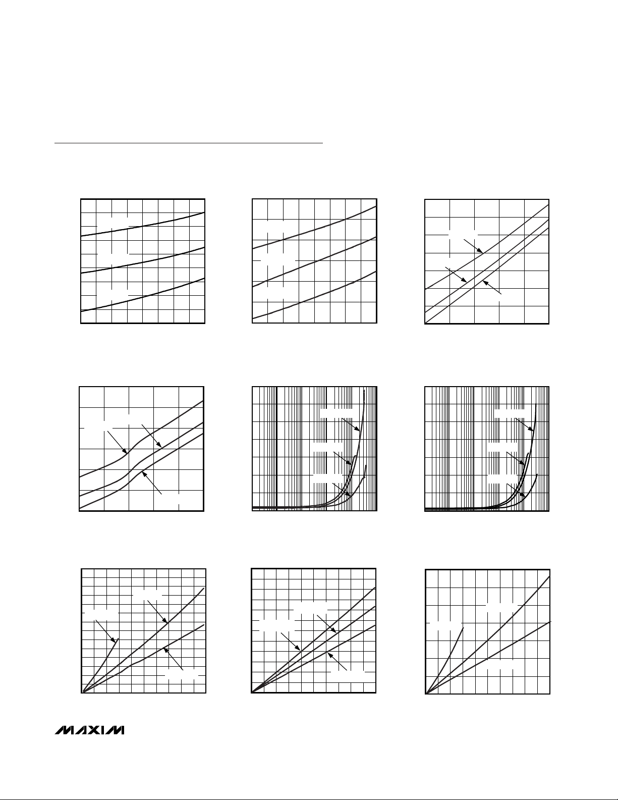
Typical Operating Characteristics
(VCC= +5V, V
EE
= 0V, CL= 15pF, V
OVERDRIVE
= 100mV, TA= +25°C, unless otherwise noted.)
Page 6

Typical Operating Characteristics (continued)
(VCC= +5V, V
EE
= 0V, CL= 15pF, V
OVERDRIVE
= 100mV, TA= +25°C, unless otherwise noted.)
MAX9117–MAX9120
SC70, 1.6V, Nanopower, Beyond-the-Rails
Comparators With/Without Reference
6 _______________________________________________________________________________________
0
0.2
0.1
0.4
0.3
0.6
0.5
042681537910
MAX9117/MAX9119 OUTPUT VOLTAGE
HIGH vs. SOURCE CURRENT AND TEMPERATURE
MAX9117-20 toc10
SOURCE CURRENT (mA)
V
CC
- V
OH
(V)
TA = +85°C
TA = +25°C
TA = -40°C
0
5
10
15
20
25
30
35
40
-40 -15 10 35 60 85
SHORT-CIRCUIT SINK CURRENT
vs. TEMPERATURE
MAX9117-20 toc11
TEMPERATURE (°C)
SINK CURRENT (mA)
VCC = +1.8V
VCC = +5V
VCC = +3V
0
5
10
15
20
25
30
35
40
-40 -15 10 35 60 85
MAX9117/MAX9119 SHORT-CIRCUIT SOURCE
CURRENT vs. TEMPERATURE
MAX9117-20 toc12
TEMPERATURE (°C)
SOURCE CURRENT (mA)
VCC = +1.8V
VCC = +3V
VCC = +5V
45
50
0.2
0.5
0.4
0.3
0.6
0.7
0.8
0.9
1.0
1.1
1.2
-40 10-15 356085
MAX9117-20 toc13
TEMPERATURE (°C)
V
OS
(mV)
VCC = +3V
VCC = +5V
VCC = +1.8V
OFFSET VOLTAGE vs. TEMPERATURE
3.0
4.0
3.5
5.5
5.0
4.5
6.0
-40 10-15 35 60 85
HYSTERESIS VOLTAGE vs. TEMPERATURE
MAX9117-20 toc14
TEMPERATURE (°C)
V
HB
(mV)
1.240
1.244
1.242
1.248
1.246
1.250
1.252
1.254
1.256
1.258
1.260
-40 10-15 356085
MAX9117/MAX9118
REFERENCE VOLTAGE vs. TEMPERATURE
MAX9117-20 toc15
TEMPERATURE (°C)
REFERENCE VOLTAGE (V)
VCC = +3V
VCC = +5V
VCC = +1.8V
1.249
1.250
1.251
1.252
1.253
1.254
1.5 2.5 3.5 4.52.0 3.0 4.0 5.0 5.5
MAX9117/MAX9118
REFERENCE VOLTAGE vs. SUPPLY VOLTAGE
MAX9117-20 toc16
SUPPLY VOLTAGE (V)
REFERENCE VOLTAGE (V)
1.240
1.242
1.244
1.246
1.248
1.250
1.252
1.254
1.256
1.258
1.260
045231 678910
MAX9117/MAX9118
REFERENCE OUTPUT VOLTAGE
vs. REFERENCE SOURCE CURRENT
MAX9117-20 toc17
SOURCE CURRENT (nA)
REFERENCE VOLTAGE (V)
VCC = +5V
VCC = +1.8V, +3V
1.240
1.242
1.244
1.246
1.248
1.250
1.252
1.254
1.256
1.258
1.260
045231 678910
MAX9117/MAX9118
REFERENCE OUTPUT VOLTAGE
vs. REFERENCE SINK CURRENT
MAX9117-20 toc18
SINK CURRENT (nA)
REFERENCE VOLTAGE (V)
VCC = +3V
VCC = +5V
VCC = +1.8V
Page 7

Typical Operating Characteristics (continued)
(VCC= +5V, V
EE
= 0V, CL= 15pF, V
OVERDRIVE
= 100mV, TA= +25°C, unless otherwise noted.)
MAX9117–MAX9120
SC70, 1.6V, Nanopower, Beyond-the-Rails
Comparators With/Without Reference
_______________________________________________________________________________________ 7
10
30
20
50
40
70
60
80
02010 30 40 50
MAX9117-20 toc23
INPUT OVERDRIVE (mV)
t
PD-
(µs)
PROPAGATION DELAY (t
PD-
)
vs. INPUT OVERDRIVE
VCC = +3V
VCC = +5V
VCC = +1.8V
0
5
10
15
20
25
30
35
40
0 1020304050
MAX9117-20 toc24
INPUT OVERDRIVE (mV)
t
PD+
(µs)
VCC = +5V
VCC = +3V
VCC = +1.8V
MAX9117/MAX9119
PROPAGATION DELAY (t
PD+
)
vs. INPUT OVERDRIVE
10 100 1000 10,000
MAX9118/MAX9120
PROPAGATION DELAY (t
PD-
)
vs. PULLUP RESISTANCE
MAX9117-20 toc25
R
PULLUP
(kΩ)
t
PD-
(µs)
15
9
10
11
12
13
14
VCC = +5V
VCC = +1.8V
VCC = +3V
10 100 1000 10,000
MAX9118/MAX9120
PROPAGATION DELAY (t
PD+
)
vs. PULLUP RESISTANCE
MAX9117-20 toc26
R
PULLUP
(kΩ)
t
PD+
(µs)
100
0
20
40
60
80
VCC = +5V
VCC = +1.8V
VCC = +3V
IN+
(50mV/div)
OUT
(2V/div)
PROPAGATION DELAY (t
PD-
)
(V
CC
= +5V)
20µs/div
MAX9117-20 toc27
OV
OV
8
14
12
10
16
18
20
22
24
26
28
MAX9117-20 toc19
TEMPERATURE (°C)
t
PD-
(µs)
PROPAGATION DELAY (t
PD-
)
vs. TEMPERATURE
-40 10-15 356085
VCC = +1.8V
VCC = +3V
VCC = +5V
0
20
10
40
30
50
60
MAX9117-20 toc20
t
PD+
(µs)
MAX9117/MAX9119
PROPAGATION DELAY (t
PD+
)
vs. TEMPERATURE
-40 10-15 35 60 85
TEMPERATURE (°C)
VCC = +5V
VCC = +1.8V
VCC = +3V
200
0
0.01 0.1 1 10 100 1000
40
MAX9117-20 toc21
CAPACITIVE LOAD (nF)
t
PD-
(µs)
80
120
160
20
60
100
140
180
PROPAGATION DELAY (t
PD-
)
vs. CAPACITIVE LOAD
VCC = +5V
VCC = +1.8V
VCC = +3V
0.01 0.1 1 10 100 1000
MAX9117-20 toc22
CAPACITIVE LOAD (nF)
t
PD+
(µs)
MAX9117/MAX9119
PROPAGATION DELAY (t
PD+
)
vs. CAPACITIVE LOAD
0
40
20
100
80
60
140
160
120
180
VCC = +5V
VCC = +1.8V
VCC = +3V
Page 8

Typical Operating Characteristics (continued)
(VCC= +5V, V
EE
= 0V, CL= 15pF, V
OVERDRIVE
= 100mV, TA= +25°C, unless otherwise noted.)
MAX9117–MAX9120
SC70, 1.6V, Nanopower, Beyond-the-Rails
Comparators With/Without Reference
8 _______________________________________________________________________________________
IN+
(50mV/div)
OUT
(1V/div)
MAX9117/MAX9119
PROPAGATION DELAY (t
PD+
)
(V
CC
= +1.8V)
20µs/div
MAX9117-20 toc32
OV
OV
IN+
(50mV/div)
OUT
(1V/div)
MAX9117/MAX9119
10kHz RESPONSE (V
CC
= +1.8V)
20µs/div
MAX9117-20 toc33
OV
OV
IN+
(50mV/div)
OUT
(2V/div)
MAX9117/MAX9119
1kHz RESPONSE (V
CC
= +5V)
200µs/div
MAX9117-20 toc34
OV
OV
V
CC
(2V/div)
OUT
(2V/div)
POWER-UP/DOWN RESPONSE
40µs/div
MAX9117-20 toc35
OV
OV
IN+
(50mV/div)
OUT
(2V/div)
PROPAGATION DELAY (t
PD-
)
(V
CC
= +3V)
20µs/div
MAX9117-20 toc29
OV
OV
IN+
(50mV/div)
OUT
(2V/div)
MAX9117/MAX9119
PROPAGATION DELAY (t
PD+
)
(V
CC
= +3V)
20µs/div
MAX9117-20 toc30
OV
OV
IN+
(50mV/div)
OUT
(1V/div)
PROPAGATION DELAY (t
PD-
)
(V
CC
= +1.8V)
20µs/div
MAX9117-20 toc31
OV
OV
IN+
(50mV/div)
OUT
(2V/div)
MAX9117/MAX9119
PROPAGATION DELAY (t
PD+
)
(V
CC
= +5V)
20µs/div
MAX9117-20 toc28
OV
OV
Page 9

MAX9117–MAX9120
SC70, 1.6V, Nanopower, Beyond-the-Rails
Comparators With/Without Reference
_______________________________________________________________________________________ 9
Functional Diagrams
MAX9117
MAX9118
IN+
OUT
V
CC
V
EE
REF
REF
1.252V
MAX9119
MAX9120
IN+
OUT
V
CC
V
EE
IN-
Detailed Description
The MAX9117/MAX9118 feature an on-board 1.252V
±1.75% reference, yet draw an ultra-low supply current
of 600nA. The MAX9119/MAX9120 (without reference)
consume just 350nA of supply current. All four devices
are guaranteed to operate down to +1.6V. Their common-mode input voltage range extends 200mV
beyond-the-rails. Internal hysteresis ensures clean output switching, even with slow-moving input signals.
Large internal output drivers allow rail-to-rail output
swing with up to ±5mA loads.
The output stage employs a unique design that minimizes supply-current surges while switching, virtually
eliminating the supply glitches typical of many other
comparators. The MAX9117/MAX9119 have a push-pull
output stage that sinks as well as sources current. The
MAX9118/MAX9120 have an open-drain output stage
that can be pulled beyond V
CC
to an absolute maximum of 6V above VEE. These open-drain versions are
ideal for implementing wire-OR output logic functions.
Input Stage Circuitry
The input common-mode voltage range extends from
V
EE
- 0.2V to VCC+ 0.2V. These comparators operate
at any differential input voltage within these limits. Input
bias current is typically ±0.15nA if the input voltage is
between the supply rails. Comparator inputs are protected from overvoltage by internal ESD protection
diodes connected to the supply rails. As the input voltage exceeds the supply rails, these ESD protection
diodes become forward biased and begin to conduct.
Output Stage Circuitry
The MAX9117–MAX9120 contain a unique breakbefore-make output stage capable of rail-to-rail operation with up to ±5mA loads. Many comparators
consume orders of magnitude more current during
switching than during steady-state operation. However,
with this family of comparators, the supply-current
change during an output transition is extremely small.
In the Typical Operating Characteristics, the Supply
Current vs. Output Transition Frequency graphs show
the minimal supply-current increase as the output
switching frequency approaches 1kHz. This characteristic reduces the need for power-supply filter capacitors to reduce glitches created by comparator
switching currents. In battery-powered applications,
this characteristic results in a substantial increase in
battery life.
PIN
M A X9117/
M A X9118
M A X91 19/
SC70
FUNCTION
1
6
1
6
OUT Comparator Output
2424V
EE
Negative Supply
3 3 3 3 IN+
Comparator
Noninverting Input
42
REF
1.252V Reference
5757V
CC
Positive Supply
——
4 2 IN-
Comparator Inverting
Input
—
8
N.C.
No Connection.
Not internally
connected.
Pin Description
M A X91 20
SO SC 70 SO
—
1, 5,
—
NAME
1, 5,
8
Page 10

MAX9117–MAX9120
SC70, 1.6V, Nanopower, Beyond-the-Rails
Comparators With/Without Reference
10 ______________________________________________________________________________________
Reference (MAX9117/MAX9118)
The internal reference in the MAX9117/MAX9118 has an
output voltage of +1.252V with respect to VEE. Its typical
temperature coefficient is 100ppm/°C over the full
-40°C to +85°C temperature range. The reference is a
PNP emitter-follower driven by a 120nA current source
(Figure 1). The output impedance of the voltage reference is typically 200kΩ, preventing the reference from
driving large loads. The reference can be bypassed with
a low-leakage capacitor. The reference is stable for any
capacitive load. For applications requiring a lower output
impedance, buffer the reference with a low-input-leakage op amp, such as the MAX4162.
Applications Information
Low-Voltage, Low-Power Operation
The MAX9117–MAX9120 are ideally suited for use with
most battery-powered systems. Table 1 lists a variety of
battery types, capacities, and approximate operating
times for the MAX9117–MAX9120, assuming nominal
conditions.
Internal Hysteresis
Many comparators oscillate in the linear region of operation because of noise or undesired parasitic feedback. This tends to occur when the voltage on one
input is equal or very close to the voltage on the other
input. The MAX9117–MAX9120 have internal hysteresis
to counter parasitic effects and noise.
The hysteresis in a comparator creates two trip points:
one for the rising input voltage (V
THR
) and one for the
falling input voltage (V
THF
) (Figure 2). The difference
between the trip points is the hysteresis (V
HB
). When
the comparator’s input voltages are equal, the hysteresis effectively causes one comparator input to move
quickly past the other, thus taking the input out of the
region where oscillation occurs. Figure 2 illustrates the
case in which IN- has a fixed voltage applied, and IN+
is varied. If the inputs were reversed, the figure would
be the same, except with an inverted output.
Additional Hysteresis (MAX9117/MAX9119)
The MAX9117/MAX9119 have a 4mV internal hysteresis
band (VHB). Additional hysteresis can be generated
with three resistors using positive feedback (Figure 3).
Unfortunately, this method also slows hysteresis response time. Use the following procedure to calculate
resistor values.
1) Select R3. Leakage current at IN is under 2nA, so the
current through R3 should be at least 0.2µA to minimize errors caused by leakage current. The current
through R3 at the trip point is (V
REF
- V
OUT
) / R3.
Considering the two possible output states in solving
for R3 yields two formulas: R3 = V
REF
/ IR3or R3 =
(VCC- V
REF
) / IR3. Use the smaller of the two result-
ing resistor values. For example, when using the
120nA
REF
V
CC
V
EE
V
BIAS
Figure 1. MAX9117/MAX9118 Voltage Reference Output
Equivalent Circuit
Table 1. Battery Applications Using MAX9117–MAX9120
BATTERY
TYPE
RECHARGEABLE
V
FRESH
(V)
V
END-OF-LIFE
(V)
CAPACITY,
AA SIZE
(mA-h)
MAX9117/MAX9118
OPERATING TIME
(hr)
Alkaline
(2 Cells)
No 3.0 1.8 2000
2.5 x 10
6
Nickel-Cadmium
(2 Cells)
Yes 2.4 1.8 750 937,500
1.25 x 10
6
10002.73.5Yes
Lithium-Ion
(1 Cell)
Nickel-Metal-
Hydride
(2 Cells)
Yes 2.4 1.8 1000
1.25 x 10
6
MAX9119/MAX9120
OPERATING TIME
(hr)
5 x 10
6
1.875 x 10
6
2.5 x 10
6
2.5 x 10
6
Page 11

MAX9117–MAX9120
SC70, 1.6V, Nanopower, Beyond-the-Rails
Comparators With/Without Reference
______________________________________________________________________________________ 11
THRESHOLDS
OUT
IN+
IN-
V
HB
HYSTERESIS
BAND
V
THF
V
THR
Figure 2. Threshold Hysteresis Band
V
CC
MAX9117
MAX9119
OUT
R3
R1
R2
V
REF
V
EE
V
IN
V
CC
Figure 3. MAX9117/MAX9119 Additional Hysteresis
MAX9117 (V
REF
= 1.252V) and VCC= +5V, and if
we choose IR3= 1µA, then the two resistor values
are 1.2MΩ and 3.8MΩ. Choose a 1.2MΩ standard
value for R3.
2) Choose the hysteresis band required (VHB). For this
example, choose 50mV.
3) Calculate R1 according to the following equation:
R1 = R3 (VHB/ VCC)
For this example, insert the values:
R1 = 1.2MΩ (50mV / 5V) = 12kΩ
4) Choose the trip point for V
IN
rising (V
THR
) such that
V
THR
> V
REF
✕
(R1 + R3) / R3, (V
THR
is the trip point
for VINrising). This is the threshold voltage at which
the comparator switches its output from low to high
as VINrises above the trip point. For this example,
choose 3V.
5) Calculate R2 as follows:
R2 = 1 / [V
THR
/ (V
REF
✕
R1) - (1 / R1) - (1 / R3)]
R2 = 1 / [3.0V / (1.252V ✕12kΩ) - (1 / 12kΩ) -
(1 / 1.2MΩ)] = 8.655kΩ
For this example, choose an 8.66kΩ standard 1% value.
6) Verify the trip voltages and hysteresis as follows:
V
IN
rising: V
THR
= V
REF
✕
R1 [(1 / R1) + (1 / R2)
+ (1 / R3)] = 3V
VINfalling: V
THF
= V
THR
- (R1 ✕VCC/ R3) = 2.95V
Hysteresis = V
THR
- V
THF
= 50mV
Additional Hysteresis (MAX9118/MAX9120)
The MAX9118/MAX9120 have a 4mV internal hysteresis
band. They have open-drain outputs and require an
external pullup resistor (Figure 4). Additional hysteresis
can be generated using positive feedback, but the formulas differ slightly from those of the MAX9117/
MAX9119. Use the following procedure to calculate
resistor values.
1) Select R3 according to the formulas R3 = V
REF
/ 1µA
or R3 = (VCC- V
REF
) / 1µA - R4. Use the smaller of
the two resulting resistor values.
2) Choose the hysteresis band required (VHB).
3) Calculate R1 according to the following equation:
R1 = (R3 + R4) (V
HB
/ VCC)
4) Choose the trip point for VINrising (V
THR
) (V
THR
is
the trip point for VINrising). This is the threshold voltage at which the comparator switches its output
from low to high as VINrises above the trip point.
5) Calculate R2 as follows:
6) Verify the trip voltages and hysteresis as follows:
Hysteresis = V
THR
- V
THF
V falling
VVR
RR RRRRR
V
IN
THF REF CC
:
=× ++
+
⎛
⎝
⎜
⎞
⎠
⎟
+
×
−1
111
2134134
Vri g V V R
RR R
IN THR REF
sin : =× ++
⎛
⎝
⎜
⎞
⎠
⎟
1
11121
3
R
V
VRRR
THR
REF
21
11113
=
×
⎛
⎝
⎜
⎞
⎠
⎟
⎡
⎣
⎢
⎢
⎤
⎦
⎥
⎥
−− /
Page 12

MAX9117–MAX9120
SC70, 1.6V, Nanopower, Beyond-the-Rails
Comparators With/Without Reference
12 ______________________________________________________________________________________
Board Layout and Bypassing
Power-supply bypass capacitors are not typically
needed, but use 100nF bypass capacitors close to the
device’s supply pins when supply impedance is high,
supply leads are long, or excessive noise is expected
on the supply lines. Minimize signal trace lengths to
reduce stray capacitance. A ground plane and surface-mount components are recommended. If the REF
pin is decoupled, use a new low-leakage capacitor.
Zero-Crossing Detector
Figure 5 shows a zero-crossing detector application.
The MAX9119’s inverting input is connected to ground,
and its noninverting input is connected to a 100mV
P-P
signal source. As the signal at the noninverting input
crosses 0V, the comparator’s output changes state.
Logic-Level Translator
The Typical Application Circuit shows an application
that converts 5V logic to 3V logic levels. The MAX9120
is powered by the +5V supply voltage, and the pullup
resistor for the MAX9120’s open-drain output is connected to the +3V supply voltage. This configuration
allows the full 5V logic swing without creating overvoltage on the 3V logic inputs. For 3V to 5V logic-level
translations, simply connect the +3V supply voltage to
VCCand the +5V supply voltage to the pullup resistor.
Chip Information
TRANSISTOR COUNT: 98
MAX9120
IN-
2MΩ
2MΩ
R
PULLUP
3V (5V)
LOGIC OUT
OUT
V
CC
+5V (+3V)
+3V (+5V)
V
EE
5V (3V) LOGIC IN
IN+
LOGIC-LEVEL
TRANSLATOR
Typical Application Circuit
V
EE
V
CC
OUT
R3
R2
R1
R4
V
REF
V
IN
V
CC
MAX9118
MAX9120
Figure 4. MAX9118/MAX9120 Additional Hysteresis
MAX9119
IN+
OUT
V
CC
100mV
P-P
V
CC
V
EE
IN-
Figure 5. Zero-Crossing Detector
Page 13

MAX9117–MAX9120
SC70, 1.6V, Nanopower, Beyond-the-Rails
Comparators With/Without Reference
______________________________________________________________________________________ 13
Package Information
(The package drawing(s) in this data sheet may not reflect the most current specifications. For the latest package outline information
go to www.maxim-ic.com/packages
.)
SC70, 5L.EPS
PACKAGE OUTLINE, 5L SC70
21-0076
1
E
1
Page 14

MAX9117–MAX9120
SC70, 1.6V, Nanopower, Beyond-the-Rails
Comparators With/Without Reference
Maxim cannot assume responsibility for use of any circuitry other than circuitry entirely embodied in a Maxim product. No circuit patent licenses are
implied. Maxim reserves the right to change the circuitry and specifications without notice at any time.
14 ____________________Maxim Integrated Products, 120 San Gabriel Drive, Sunnyvale, CA 94086 408-737-7600
© 2007 Maxim Integrated Products is a registered trademark of Maxim Integrated Products, Inc.
SOICN .EPS
PACKAGE OUTLINE, .150" SOIC
1
1
21-0041
B
REV.DOCUMENT CONTROL NO.APPROVAL
PROPRIETARY INFORMATION
TITLE:
TOP VIEW
FRONT VIEW
MAX
0.010
0.069
0.019
0.157
0.010
INCHES
0.150
0.007
E
C
DIM
0.014
0.004
B
A1
MIN
0.053A
0.19
3.80 4.00
0.25
MILLIMETERS
0.10
0.35
1.35
MIN
0.49
0.25
MAX
1.75
0.050
0.016L
0.40 1.27
0.3940.386D
D
MINDIM
D
INCHES
MAX
9.80 10.00
MILLIMETERS
MIN
MAX
16
AC
0.337 0.344 AB8.758.55 14
0.189 0.197 AA5.004.80 8
N MS012
N
SIDE VIEW
H 0.2440.228 5.80 6.20
e 0.050 BSC 1.27 BSC
C
HE
e
B
A1
A
D
0∞-8∞
L
1
VARIATIONS:
Package Information (continued)
(The package drawing(s) in this data sheet may not reflect the most current specifications. For the latest package outline information
go to www.maxim-ic.com/packages
.)
Revision History
Pages changed at Rev 4: 1, 2, 9, 13
 Loading...