

Page 1
For pricing, delivery, and ordering information, please contact Maxim Direct at 1-888-629-4642,
or visit Maxim's website at www.maxim-ic.com.
General Description
The MAX9111/MAX9113 single/dual low-voltage differential signaling (LVDS) receivers are designed for highspeed applications requiring minimum power
consumption, space, and noise. Both devices support
switching rates exceeding 500Mbps while operating from
a single +3.3V supply, and feature ultra-low 300ps (max)
pulse skew required for high-resolution imaging applications such as laser printers and digital copiers.
The MAX9111 is a single LVDS receiver, and the
MAX9113 is a dual LVDS receiver.
Both devices conform to the EIA/TIA-644 LVDS standard
and convert LVDS to LVTTL/CMOS-compatible outputs.
A fail-safe feature sets the outputs high when the inputs
are undriven and open, terminated, or shorted. The
MAX9111/MAX9113 are available in space-saving 8-pin
SOT23 and SO packages. Refer to the MAX9110/
MAX9112 data sheet for single/dual LVDS line drivers.
________________________Applications
Features
o Low 300ps (max) Pulse Skew for High-Resolution
Imaging and High-Speed Interconnect
o Space-Saving 8-Pin SOT23 and SO Packages
o Pin-Compatible Upgrades to DS90LV018A and
DS90LV028A (SO Packages Only)
o Guaranteed 500Mbps Data Rate
o Low 29mW Power Dissipation at 3.3V
o Conform to EIA/TIA-644 Standard
o Single +3.3V Supply
o Flow-Through Pinout Simplifies PCB Layout
o Fail-Safe Circuit Sets Output High for Undriven
Inputs
o High-Impedance LVDS Inputs when Powered Off
MAX9111/MAX9113
Single/Dual LVDS Line Receivers with
Ultra-Low Pulse Skew in SOT23
________________________________________________________________
Maxim Integrated Products
1
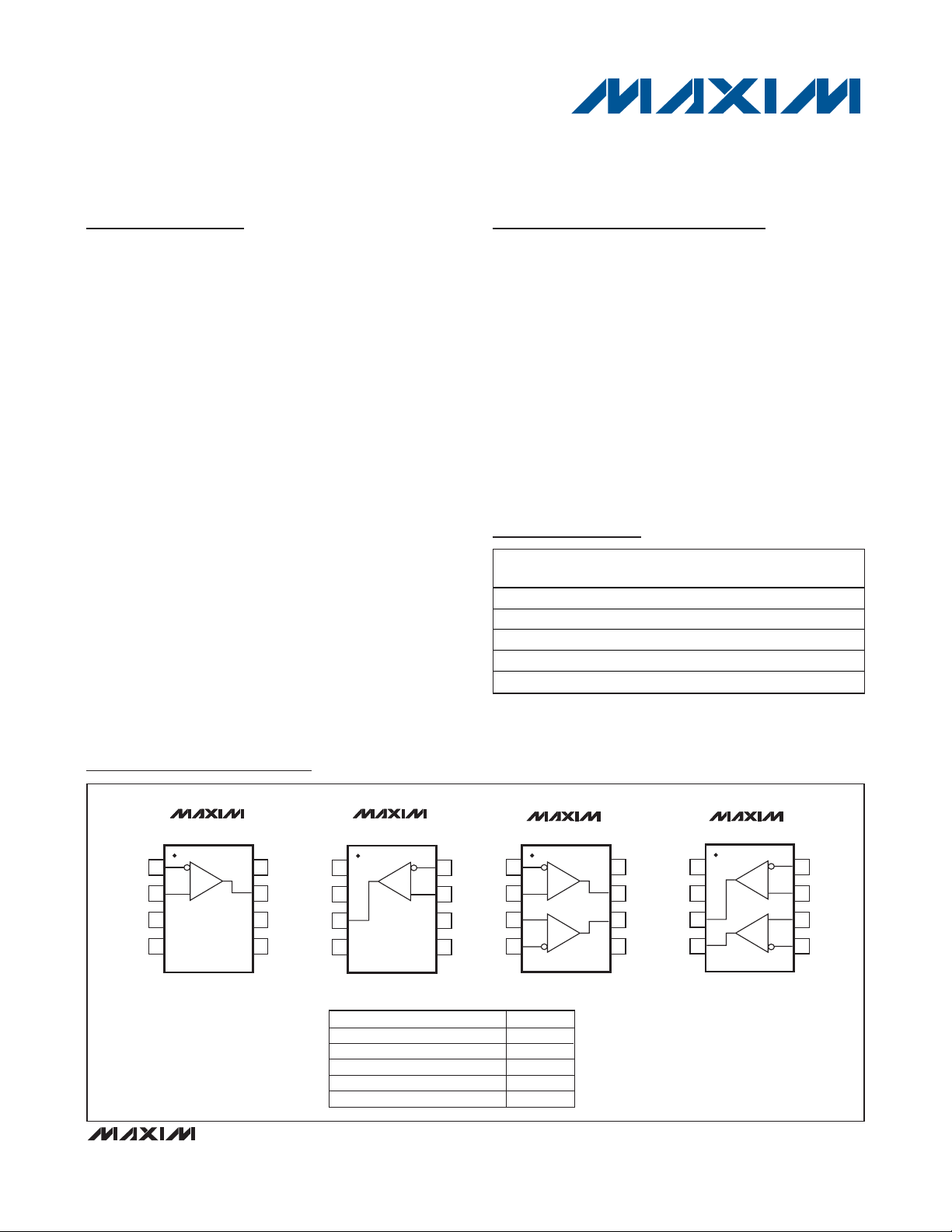
Pin Configurations/Functional Diagrams/Truth Table
19-1803; Rev 3; 3/09
Ordering Information
Laser Printers
Digital Copiers
Cellular Phone
Base Stations
Telecom Switching
Equipment
Network Switches/Routers
LCD Displays
Backplane Interconnect
Clock Distribution
Typical Operating Circuit appears at end of data sheet.
/V denotes an automotive qualified part.
+
Denotes a lead(Pb)-free/RoHS-compliant package.
PART
TEMP
RANGE
MAX9111EKA -40°C to +85°C 8 SOT23 AAEE
MAX9111ESA -40°C to +85°C 8 SO —
MAX9113EKA -40°C to +85°C 8 SOT23 AAED
MAX9113ESA -40°C to +85°C 8 SO —
MAX9113ASA/V+ -40°C to +125°C 8 SO —
PINPACKAGE
TOP
MARK
N.C.
MAX9111MAX9111
IN1-
IN2+
1
2
3
4
SO
OUT_
H
L
H
H
H
1
IN-
2
3
4
SO
87V
6
5
OUTIN+
N.C.
GNDN.C.
V
CC
1
CC
GND
2
3
OUT
N.C.
MAX9111
4
SOT23
(IN_+) - (IN_-)
100Ω PARALLEL TERMINATION (UNDRIVEN)
≥ 100mV
≥
-100mV
OPEN
SHORT
8
IN-
7
IN+
6
N.C.
5
N.C.
87V
6
5
H = LOGIC LEVEL HIGH
L = LOGIC LEVEL LOW
V
CC
CC
GND
OUT1IN1+
OUT1
OUT2
OUT2
GNDIN2-
MAX9113MAX9113
1
2
3
4
SOT23
87IN1-
IN1+
6
IN2+
5
IN2-
Page 2
MAX9111/MAX9113
Single/Dual LVDS Line Receivers with
Ultra-Low Pulse Skew in SOT23
2 _______________________________________________________________________________________
ABSOLUTE MAXIMUM RATINGS
ELECTRICAL CHARACTERISTICS
(VCC= +3.0V to +3.6V, magnitude of input voltage, |VID| = +0.1V to +1.0V, VCM= |VID|/2 to (2.4V - (|VID|/2)), TA= T
MIN
to T
MAX
.
Typical values are at V
CC
= +3.3V and TA= +25°C, unless otherwise noted.) (Notes 1, 2)
Stresses beyond those listed under “Absolute Maximum Ratings” may cause permanent damage to the device. These are stress ratings only, and functional
operation of the device at these or any other conditions beyond those indicated in the operational sections of the specifications is not implied. Exposure to
absolute maximum rating conditions for extended periods may affect device reliability.
VCCto GND..............................................................-0.3V to +4V
IN_ _ to GND .........................................................-0.3V to +3.9V
OUT_ _ to GND...........................................-0.3V to (V
CC
+ 0.3V)
ESD Protection All Pins
(Human Body Model, IN_+, IN_-) ..................................±11kV
Continuous Power Dissipation (T
A
= +70°C)
8-Pin SOT23 (derate 8.9mW/°C above +70°C)............714mW
8-Pin SO (derate 5.88mW°C above +70°C).................471mW
Operating Temperature Ranges
MAX911_E .......................................................-40°C to +85°C
MAX911_A .....................................................-40°C to +125°C
Storage Temperature Range .............................-65°C to +150°C
Lead Temperature (soldering, 10s) .................................+300°C
PARAMETER SYMBOL CONDITIONS MIN TYP MAX UNITS
Differential Input High Threshold
(Note 3)
Differential Input Low Threshold
(Note 3)
Differential Input Resistance R
Output High Voltage (OUT_) V
Output Low Voltage (OUT_) V
Output Short-Circuit Current I
No-Load Supply Current I
V
V
DIFF
OH
OS
CC
TH
TL
OL
V
= 0.05V, 1.2V, 2.75V at 3.3V 100 mV
CM
V
= 0.05V, 1.2V, 2.75V at 3.3V -100 mV
CM
VCM = 0.2V or 2.2V, VID = ±0.4V,
V
= 0 or 3.6V
CC
I
= -4mA
OH
I
= 4mA, VID = -200mV 0.4
OL
VID = +200mV, V
MAX9111 4.2 6
MAX9113 8.7 11
518 kΩ
VID = +200mV 2.7
Inputs shorted,
undriven
100Ω parallel
termination,
undriven
_ = 0 -100 mA
OUT
2.7
2.7
V
mA
Page 3

MAX9111/MAX9113
Single/Dual LVDS Line Receivers with
Ultra-Low Pulse Skew in SOT23
_______________________________________________________________________________________ 3
SWITCHING CHARACTERISTICS
(VCC= +3.0V to +3.6V, TA= T
MIN
to T
MAX
. Typical values are at VCC= +3.3V and TA= +25°C, unless otherwise noted.) (Notes 4, 5, 6)
Note 1: Maximum and minimum limits over temperature are guaranteed by design and characterization. Devices are production
tested at T
A
= +25°C.
Note 2: Current into the device is defined as positive. Current out of the devices is defined as negative. All voltages are referenced
to ground except V
TH
and VTL.
Note 3: Guaranteed by design, not production tested.
Note 4: AC parameters are guaranteed by design and characterization.
Note 5: C
L
includes probe and test jig capacitance.
Note 6: f
MAX
generator output conditions: tR= tF< 1ns (0 to 100%), 50% duty cycle, VOH= 1.3V, VOL= 1.1V.
Note 7: t
SKD1
is the magnitude difference of differential propagation delays in a channel. t
SKD1
= |t
PLHD
- t
PHLD
|.
Note 8: t
SKD2
is the magnitude difference of the t
PLHD
or t
PHLD
of one channel and the t
PLHD
or t
PHLD
of the other channel on the
same device.
Note 9: t
SKD3
is the magnitude difference of any differential propagation delays between devices at the same VCCand within 5°C
of each other.
Note 10: t
SKD4
, is the magnitude difference of any differential propagation delays between devices operating over the rated supply
and temperature ranges.
PARAMETER SYMBOL CONDITIONS MIN TYP MAX UNITS
Differential Propagation Delay
High to Low
Differential Propagation Delay
Low to High
Differential Pulse Skew
|t
- t
PHLD
| (Note 7)
PLHD
Differential Channel-to-Channel
Skew; Same Device (MAX9113
only) (Note 8)
Differential Part-to-Part Skew
(Note 9)
Differential Part-to-Part Skew
(MAX9113 only) (Note 10)
Rise Time t
Fall Time t
t
PHLD
t
PLHD
t
SKD1
t
SKD2
t
SKD3
t
SKD4
TLH
THL
CL = 15pF, VID =
±200mV, V
CM
= 1.2V
(Figures 1, 2)
CL = 15pF, VID =
±200mV, V
CM
= 1.2V
(Figures 1, 2)
TA = +85°C 1.0 1.77 2.5
= +125°C 3.0
T
A
TA = +85°C 1.0 1.68 2.5
T
= +125°C 3.0
A
CL = 15pF, VID = ±200mV, VCM = 1.2V
(Figures 1, 2)
CL = 15pF, VID =
±200mV, V
CM
= 1.2V
(Figures 1, 2)
CL = 15pF, VID =
±200mV, V
CM
= 1.2V
(Figures 1, 2)
TA = +85°C 0.6 0.8
= +125°C 1.0
T
A
TA = +85°C 0.6 0.8
T
= +125°C 1.0
A
ns
ns
90 300 ps
140 400 ps
1ns
1.5 ns
ns
ns
All channels switching, CL = 15pF,
V
Maximum Operating Frequency f
MAX
(max) = 0.4V, V
OL
(min) = 2.7V,
OH
250 300 MHz
40% < duty cycle < 60% (Note 6)
Page 4

Test Circuit Diagrams
MAX9111/MAX9113
Single/Dual LVDS Line Receivers with
Ultra-Low Pulse Skew in SOT23
4 _______________________________________________________________________________________
Figure 1. Receiver Propagation Delay and Transition Time Test Circuit
Figure 2. Receiver Propagation Delay and Transition Time Waveforms
IN_+
GENERATOR
IN_-
R
OUT_
C
L
50Ω
IN_-
0V
DIFFERENTIAL
IN_+
t
PLHD
OUT_
20%
t
TLH
50Ω
+1.3V
VID = 200mV
80%
50% 50%
80%
+1.2V
t
PHLD
t
+1.1V
THL
20%
V
OH
V
OL
Page 5

MAX9111/MAX9113
Single/Dual LVDS Line Receivers with
Ultra-Low Pulse Skew in SOT23
_______________________________________________________________________________________ 5
Typical Operating Characteristics
(VCC= 3.3V, |VID| = 200mV, VCM= 1.2V, fIN= 200MHz, CL= 15pF, TA= +25°C and over recommended operating conditions,
unless otherwise specified.)
3.0 3.23.1 3.3 3.4 3.5 3.6
MAX9111 toc01
SUPPLY VOLTAGE (V)
OUTPUT HIGH VOLTAGE (V)
OUTPUT HIGH VOLTAGE
vs. SUPPLY VOLTAGE
2.5
2.7
2.6
2.8
2.9
3.0
3.1
3.2
3.3
3.4
3.5
3.6
3.7
I
OUT_
= 4mA
3.0 3.2 3.33.1 3.4 3.5 3.6
MAX9111 toc02
SUPPLY VOLTAGE (V)
OUTPUT LOW VOLTAGE (mV)
OUTPUT LOW VOLTAGE
vs. SUPPLY VOLTAGE
130
120
110
100
90
I
OUT_
= 4mA
48
58
53
68
63
78
73
83
3.0 3.2 3.33.1 3.4 3.5 3.6
MAX9111 toc03
SUPPLY VOLTAGE (V)
OUTPUT SHORT-CIRCUIT CURRENT (mA)
OUTPUT SHORT-CIRCUIT CURRENT
vs. SUPPLY VOLTAGE
VID = 200mV
14
16
20
18
22
24
3.0 3.23.1 3.3 3.4 3.5 3.6
MAX9111 toc04
SUPPLY VOLTAGE (V)
DIFFERENTIAL THRESHOLD VOLTAGE (mV)
DIFFERENTIAL THRESHOLD VOLTAGE
vs. SUPPLY VOLTAGE
HIGH-LOW
LOW-HIGH
0.01 0.1 1 10 100 1000
MAX9111 toc05
FREQUENCY (MHz)
POWER-SUPPLY CURRENT (mA)
0
20
10
40
30
50
60
BOTH CHANNELS SWITCHING
ONE SWITCHING
MAX9113 POWER-SUPPLY CURRENT
vs. FREQUENCY
-40 10-15 35 60 85
MAX9111 toc06
TEMPERATURE (°C)
POWER-SUPPLY CURRENT (mA)
POWER-SUPPLY CURRENT
vs. TEMPERATURE
6.5
6.7
6.6
6.8
6.9
7.0
7.1
7.2
7.3
7.4
7.5
7.6
7.7
fIN = 1MHz
BOTH CHANNELS SWITCHING
1.50
1.60
1.55
1.65
1.70
1.75
1.80
1.85
1.90
1.95
2.00
2.05
2.10
3.0 3.1 3.2 3.43.3 3.5 3.6
DIFFERENTIAL PROPAGATION DELAY
vs. SUPPLY VOLTAGE
MAX9111 toc07
SUPPLY VOLTAGE (V)
DIFFERENTIAL PROPAGATION DELAY (ns)
t
PHLD
t
PLHD
1.50
1.60
1.55
1.65
1.75
1.70
1.80
1.85
1.90
2.00
1.95
2.05
2.10
2.15
2.20
-40-1510356085
DIFFERENTIAL PROPAGATION DELAY
vs. TEMPERATURE
MAX9111 toc08
TEMPERATURE (°C)
DIFFERENTIAL PROPAGATION DELAY (ns)
t
PHLD
t
PLHD
120
100
80
60
40
3.0 3.33.1 3.2 3.4 3.5 3.6
DIFFERENTIAL PULSE SKEW
vs. SUPPLY VOLTAGE
MAX9111 toc09
SUPPLY VOLTAGE (V)
DIFFERENTIAL SKEW (ns)
Page 6

MAX9111/MAX9113
Single/Dual LVDS Line Receivers with
Ultra-Low Pulse Skew in SOT23
6 _______________________________________________________________________________________
Typical Operating Characteristics (continued)
200
600
1000
1400
1800
2200
10 2015 25 30 35 40 45 50
TRANSITION TIME vs. LOAD
MAX9111 toc16
LOAD (pF)
TRANSITION TIME (ps)
t
THL
t
TLH
(VCC= 3.3V, |VID| = 200mV, VCM= 1.2V, fIN= 200MHz, CL= 15pF, TA= +25°C and over recommended operating conditions,
unless otherwise specified.)
DIFFERENTIAL PULSE SKEW
vs. TEMPERATURE
250
200
150
100
DIFFERENTIAL SKEW (ps)
50
0
-40 10-15 35 60 85
TEMPERATURE (°C)
MAX9111 toc10
DIFFERENTIAL PROPAGATION DELAY
vs. DIFFERENTIAL INPUT VOLTAGE
3.0
fIN = 20MHz
2.8
2.6
2.4
2.2
2.0
1.8
1.6
1.4
DIFFERENTIAL PROPAGATION DELAY (ns)
1.2
1.0
0 1000500 1500 2000 2500
DIFFERENTIAL INPUT VOLTAGE (mV)
t
PHLD
t
PLHD
DIFFERENTIAL PROPAGATION DELAY
vs. COMMON-MODE VOLTAGE
2.2
fIN = 20MHz
2.1
MAX9111 toc11
2.0
1.9
1.8
1.7
DIFFERENTIAL PROPAGATION DELAY (ns)
1.6
0 1.0 1.50.5 2.0 2.5 3.0
COMMON-MODE VOLTAGE (V)
t
PHLD
t
PLHD
MAX91111 toc12
TRANSITION TIME vs. TEMPERATURE
680
t
630
580
530
480
TRANSITION TIME (ps)
430
380
330
-40 10-15 356085
TEMPERATURE (°C)
THL
t
TLH
MAX9111 toc14
DIFFERENTIAL PROPAGATION DELAY
vs. LOAD
3.1
2.9
2.7
2.5
2.3
2.1
1.9
1.7
DIFFERENTIAL PROPAGATION DELAY (ns)
1.5
10 20 2515 30 35 40 45 50
LOAD (pF)
t
PHLD
t
PLHD
MAX9111 toc15
Page 7

MAX9111/MAX9113
Single/Dual LVDS Line Receivers with
Ultra-Low Pulse Skew in SOT23
_______________________________________________________________________________________ 7
_______________Detailed Description
LVDS Inputs
The MAX9111/MAX9113 feature LVDS inputs for interfacing high-speed digital circuitry. The LVDS interface
standard is a signaling method intended for point-topoint communication over a controlled impedance
media, as defined by the ANSI/EIA/TIA-644 standards.
The technology uses low-voltage signals to achieve fast
transition times, minimize power dissipation, and noise
immunity. Receivers such as the MAX9111/MAX9113
convert LVDS signals to CMOS/LVTTL signals at rates
in excess of 500Mbps. The devices are capable of
detecting differential signals as low as 100mV and as
high as 1V within a 0V to 2.4V input voltage range . The
LVDS standard specifies an input voltage range of 0 to
2.4V referenced to ground.
Fail-Safe
The fail-safe feature sets the output to a high state
when the inputs are undriven and open, terminated, or
shorted. When using one channel in the MAX9113,
leave the unused channel open. The fail-safe feature is
not guaranteed to be operational above +85°C.
ESD Protection
As with all Maxim devices, ESD-protection structures are
incorporated on all pins to protect against electrostatic
discharges encountered during handling and assembly.
The receiver inputs of the MAX9111/MAX9113 have extra
protection against static electricity. Maxim’s engineers
have developed state-of-the-art structures to protect
these pins against ESD of ±11kV without damage. The
ESD structures withstand high ESD in all states: normal
operation, shutdown, and powered down.
ESD protection can be tested in various ways; the
receiver inputs of this product family are characterized
for protection to the limit of ±11kV using the Human
Body Model.
Human Body Model
Figure 3a shows the Human Body Model, and Figure
3b shows the current waveform it generates when discharged into a low impedance. This model consists of a
100pF capacitor charged to the ESD voltage of interest,
which is then discharged into the test device through a
1.5kΩ resistor.
Pin Description
PIN
MAX9111 MAX9113
SOT23-8 SO-8 SOT23-8 SO-8
1818VCCPower Supply
2525GNDGround
8181IN-/IN1- Receiver Inverting Differential Input
7272IN+/IN1+ Receiver Noninverting Differential Input
— — 5 4 IN2- Receiver Inverting Differential Input
— — 6 3 IN2+ Receiver Noninverting Differential Input
3737OUT/OUT1 Receiver Output
— — 4 6 OUT2 Receiver Output
4, 5, 6 3, 4, 6 — — N.C. No Connection. Not internally connected.
NAME FUNCTION
Page 8

__________ Applications Information
Supply Bypassing
Bypass VCCwith high-frequency surface-mount ceramic 0.1µF and 0.001µF capacitors in parallel, as close to
the device as possible, with the 0.001µF valued capacitor the closest to the device. For additional supply
bypassing, place a 10µF tantalum or ceramic capacitor
at the point where power enters the circuit board.
Differential Traces
Output trace characteristics affect the performance of
the MAX9111/MAX9113. Use controlled impedance
traces to match trace impedance to both transmission
medium impedance and the termination resistor.
Eliminate reflections and ensure that noise couples as
common mode by running the differential traces close
together. Reduce skew by matching the electrical
length of the traces. Excessive skew can result in a
degradation of magnetic field cancellation.
Maintain the distance between the differential traces to
avoid discontinuities in differential impedance. Avoid
90° turns and minimize the number of vias to further
prevent impedance discontinuities.
Cables and Connectors
Transmission media should have a differential characteristic impedance of about 100Ω. Use cables and connectors that have matched impedance to minimize
impedance discontinuities.
Avoid the use of unbalanced cables such as ribbon or
simple coaxial cable. Balanced cables such as twisted
pair offer superior signal quality and tend to generate
less EMI due to canceling effects. Balanced cables
tend to pick up noise as common mode, which is
rejected by the LVDS receiver.
Termination
The MAX9111/MAX9113 input differential voltage
depends on the driver current and termination resistance. Refer to the MAX9110/MAX9112 differential driver data sheet for this information.
Minimize the distance between the termination resistor
and receiver inputs. Use a single 1% to 2% surfacemount resistor across the receiver inputs.
Board Layout
For LVDS applications, a four-layer PCB that provides
separate power, ground, LVDS signals, and input signals is recommended. Isolate the input and LVDS signals from each other to prevent coupling. For best
results, separate the input and LVDS signal planes with
the power and ground planes.
MAX9111/MAX9113
Single/Dual LVDS Line Receivers with
Ultra-Low Pulse Skew in SOT23
8 _______________________________________________________________________________________
Figure 3a. Human Body ESD Test Modules Figure 3b. Human Body Current Waveform
R
C
1M
Ω
CHARGE-CURRENT
LIMIT RESISTOR
HIGH-
VOLTAGE
DC
SOURCE
100pF
C
s
R
D
1500
Ω
DISCHARGE
RESISTANCE
STORAGE
CAPACITOR
DEVICE
UNDER
TEST
AMPERES
IP 100%
90%
36.8%
10%
0
0
t
RL
TIME
CURRENT WAVEFORM
PEAK-TO-PEAK RINGING
I
r
(NOT DRAWN TO SCALE)
t
DL
Page 9

MAX9111/MAX9113
Single/Dual LVDS Line Receivers with
Ultra-Low Pulse Skew in SOT23
_______________________________________________________________________________________ 9
Typical Operating Circuit
Chip Information
PROCESS: CMOS
Package Information
For the latest package outline information and land patterns, go
to www.maxim-ic.com/packages
.
PACKAGE TYPE PACKAGE CODE DOCUMENT NO.
8 SOT23 K8-1
21-0078
8 SO S8-2
21-0041
+3.3V
0.001μF 0.1μF
DIN_
LVDS
MAX9110
MAX9112
+3.3V
0.001μF 0.1μF
RT = 100Ω
RECEIVERDRIVER
MAX9111
MAX9113
OUT_
Page 10

MAX9111/MAX9113
Single/Dual LVDS Line Receivers with
Ultra-Low Pulse Skew in SOT23
Maxim cannot assume responsibility for use of any circuitry other than circuitry entirely embodied in a Maxim product. No circuit patent licenses are
implied. Maxim reserves the right to change the circuitry and specifications without notice at any time.
10
____________________Maxim Integrated Products, 120 San Gabriel Drive, Sunnyvale, CA 94086 408-737-7600
© 2009 Maxim Integrated Products Maxim is a registered trademark of Maxim Integrated Products, Inc.
Revision History
REVISION
NUMBER
0 — Initial release —
1 2/07 — 1, 2, 8, 10, 11
2 12/07
3 3/09 Added /V designation to Ordering Information and updated Termination section. 1, 8
REVISION
DATE
DESCRIPTION
Updated Ordering Information, temperature, Switching Characteristics, Fail-Safe
section.
PAGES
CHANGED
1, 2, 3, 7
 Loading...