

Page 1
General Description
The MAX9110/MAX9112 single/dual low-voltage differential signaling (LVDS) transmitters are designed for
high-speed applications requiring minimum power consumption, space, and noise. Both devices support
switching rates exceeding 500Mbps while operating
from a single +3.3V supply, and feature ultra-low 250ps
(max) pulse skew required for high-resolution imaging
applications, such as laser printers and digital copiers.
The MAX9110 is a single LVDS transmitter, and the
MAX9112 is a dual LVDS transmitter.
Both devices conform to the EIA/TIA-644 LVDS standard.
They accept LVTTL/CMOS inputs and translate them to
low-voltage (350mV) differential outputs, minimizing electromagnetic interference (EMI) and power dissipation.
These devices use a current-steering output stage, minimizing power consumption, even at high data rates. The
MAX9110/MAX9112 are available in space-saving 8-pin
SOT23 and SO packages. Refer to the MAX9111/
MAX9113 data sheet for single/dual LVDS line receivers.
________________________Applications
Features
♦ Low 250ps (max) Pulse Skew for High-Resolution
Imaging and High-Speed Interconnect
♦ Space-Saving 8-Pin SOT23 and SO Packages
♦ Pin-Compatible Upgrades to DS90LV017/017A
and DS90LV027/027A (SO Packages)
♦ Guaranteed 500Mbps Data Rate
♦ Low 22mW Power Dissipation at 3.3V
(31mW for MAX9112)
♦ Conform to EIA/TIA-644 Standard
♦ Single +3.3V Supply
♦ Flow-Through Pinout Simplifies PC Board Layout
♦ Driver Outputs High Impedance when Powered Off
MAX9110/MAX9112
Single/Dual LVDS Line Drivers with
Ultra-Low Pulse Skew in SOT23
________________________________________________________________ Maxim Integrated Products 1
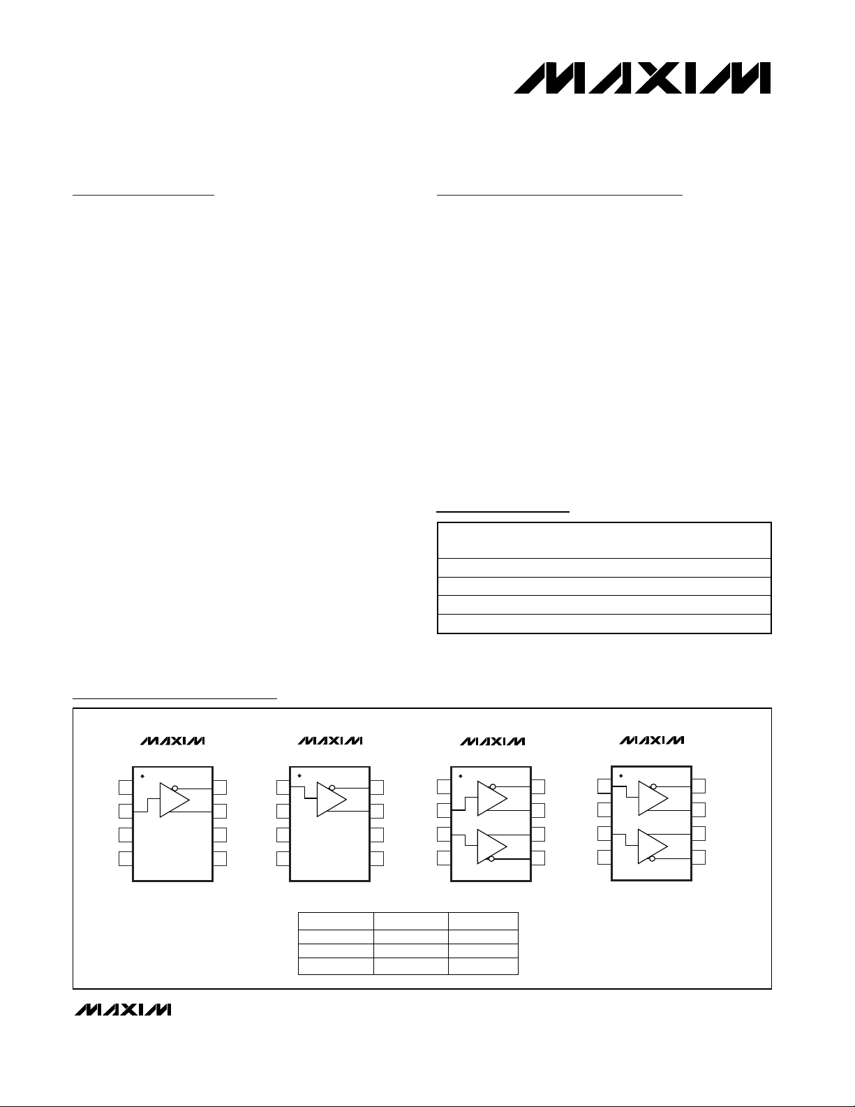
Pin Configurations/Functional Diagrams/Truth Table
19-1771; Rev 0; 9/00
For free samples and the latest literature, visit www.maxim-ic.com or phone 1-800-998-8800.
For small orders, phone 1-800-835-8769.
Ordering Information
Laser Printers
Digital Copiers
Cellular Phone Base
Stations
Telecom Switching
Equipment
Network Switches/Routers
LCD Displays
Backplane Interconnect
Clock Distribution
Typical Operating Circuit appears at end of data sheet.
PART
TEMP.
RANGE
MAX9110EKA-T -40°C to +85°C 8 SOT23-8 AADN
MAX9110ESA -40°C to +85°C 8 SO —
MAX9112EKA-T -40°C to +85°C 8 SOT23-8 AADO
MAX9112ESA -40°C to +85°C 8 SO —
PINPACKAGE
TOP
MARK
TOP VIEW
V
CC
N.C.
MAX9110
1
2
3
4
SO
87DO-
DO+DIN
N.C.
6
N.C.GND
5
MAX9112
1
2
3
4
SOT23
87DO1-
DO1+GND
DO2+
6
DO2-V
5
DIN
N.C.
MAX9110
DO+GND
N.C.
N.C.V
DO_+
L
H
V
DIN2
CC
1
2
3
4
CC
SOT23
DIN_
0.8V < V
DIN
87DO-
6
5
L
H
_ < 2.0V
MAX9112
1
2
3
4
SO
DO_-
H
L
XX
DIN1
87DO1-
DO1+DIN1
DIN2
DO2+
6
DO2-GND
5
CC
H = LOGIC LEVEL HIGH
L = LOGIC LEVEL LOW
X = UNDETERMINED
Page 2
MAX9110/MAX9112
Single/Dual LVDS Line Drivers with
Ultra-Low Pulse Skew in SOT23
2 _______________________________________________________________________________________
ABSOLUTE MAXIMUM RATINGS
ELECTRICAL CHARACTERISTICS
(VCC= +3.0V to +3.6V, RL= 100Ω ±1%, TA= -40°C to +85°C, unless otherwise noted. Typical values are at VCC= +3.3V, TA=
+25°C.) (Notes 1, 2)
AC CHARACTERISTICS
(VCC= +3.0V to +3.6V, RL= 100Ω ±1%, CL= 5pF, TA= -40°C to +85°C, unless otherwise noted. Typical values are at VCC= +3.3V,
T
A
= +25°C.) (Notes 3, 4, 5; Figures 2, 3)
Stresses beyond those listed under “Absolute Maximum Ratings” may cause permanent damage to the device. These are stress ratings only, and functional
operation of the device at these or any other conditions beyond those indicated in the operational sections of the specifications is not implied. Exposure to
absolute maximum rating conditions for extended periods may affect device reliability.
Supply Voltage (VCCto GND) ..................................-0.3V to +4V
Input Voltage (V
DIN_
to GND).....................-0.3V to (VCC+ 0.3V)
Output Voltage (V
DO
_+, VDO_- to GND or VCC) ...-0.3V to +3.9V
Output Short-Circuit Duration
(DO_+, DO_- to V
CC
or GND) ................................Continuous
ESD Protection (Human Body Model, DO_+, DO_-)..........±11kV
Continuous Power Dissipation (T
A
= +70°C)
8-Pin SOT23 (derate 7.52mW/°C above +70°C)...........602mW
8-Pin SO (derate 5.88mW/°C above +70°C)...............471mW
Operating Temperature Range ...........................-40°C to +85°C
Storage Temperature Range .............................-65°C to +150°C
Lead Temperature (soldering,10s) ..................................+300°C
)
)
Differential Output Voltage V
Change in Magnitude of Output
Voltage for Complementary
Output States
Offset Voltage V
Change in Magnitude of Offset
Voltage for Complementary
Output States
Power-Off Leakage Current I
Short-Circuit Output Current I
Input High Voltage V
Input Low Voltage V
Input Current High I
Input Current Low I
No-Load Supply Current I
Supply Current I
PARAMETER SYMBOL CONDITIONS MIN TYP MAX UNITS
Figure 1 250 350 450 mV
OD
ΔV
ΔV
O(OFF
O(SHORT
CC
CC
Figure 1 0 2 35 mV
OD
Figure 1 1.125 1.25 1.375 V
OS
Figure 1 0 2 25 mV
OS
VDO_ _ = 0 or VCC, VCC = 0 or open -10 +10 µA
DIN_ = VCC, V
DIN_ = GND, V
IH
IL
DIN_ = VCC or 2V 0 10 20 µA
IH
DIN_ = GND or 0.8V -20 -3 0 µA
IL
No load, DIN_ = VCC or 0 4.5 6 mA
DIN_ = VCC or 0
DO_+
DO
= 0 or
_- = 0
MAX9110 6.7 8
MAX9112 9.4 13
-20 mA
2.0 V
GND 0.8 V
CC
V
mA
Differential High-to-Low
Propagation Delay
Differential Low-to-High
Propagation Delay
Differential Pulse Skew
|t
C hannel- to-C hannel S kew ( N ote 7) t
PARAMETER SYMBOL CONDITIONS MIN TYP MAX UNITS
PHLD
- t
PLHD
| (Note 6)
t
PHLD
t
PLHD
t
SKD1
SKD2
1 1.54 2.5 ns
1 1.58 2.5 ns
40 250 ps
70 400 ps
Page 3
MAX9110/MAX9112
Single/Dual LVDS Line Drivers with
Ultra-Low Pulse Skew in SOT23
_______________________________________________________________________________________ 3
AC CHARACTERISTICS (continued)
(VCC= +3.0V to +3.6V, RL= 100Ω ±1%, CL= 5pF, TA= -40°C to +85°C, unless otherwise noted. Typical values are at VCC= +3.3V,
T
A
= +25°C.) (Notes 3, 4, 5; Figures 2, 3)
Note 1: Maximum and minimum limits over temperature are guaranteed by design. Devices are production tested at T
A
= +25°C.
Note 2: By definition, current into the device is positive and current out of the device is negative. Voltages are referred to device
ground except V
OD
.
Note 3: AC parameters are guaranteed by design and characterization.
Note 4: C
L
includes probe and fixture capacitance.
Note 5: Signal generator conditions for dynamic tests: V
OL
= 0, VOH= 3V, f = 20MHz, 50% duty cycle, RO= 50Ω, tR≤ 1ns, and tF≤
1ns (0 to 100%).
Note 6: t
SKD1
is the magnitude difference of differential propagation delays in a channel; t
SKD1
= | t
PHLD
- t
PLHD
|.
Note 7: t
SKD2
is the magnitude difference of the t
PLHD
or t
PHLD
of one channel and the t
PLHD
or t
PHLD
of the other channel on the
same device (MAX9112).
Note 8: t
SKD3
is the magnitude difference of any differential propagation delays between devices at the same VCCand within 5°C
of each other.
Note 9: t
SKD4
is the magnitude difference of any differential propagation delays between devices operating over the rated supply
and temperature ranges.
Note 10:f
MAX
signal generator conditions: V
OL
= 0, VOH= +3V, frequency = 250MHz, tR≤ 1ns, tF≤ 1ns (0 to 100%) 50% duty cycle.
Transmitter output criteria: duty cycle = 45% to 55%, V
OD
≥ 250mV.
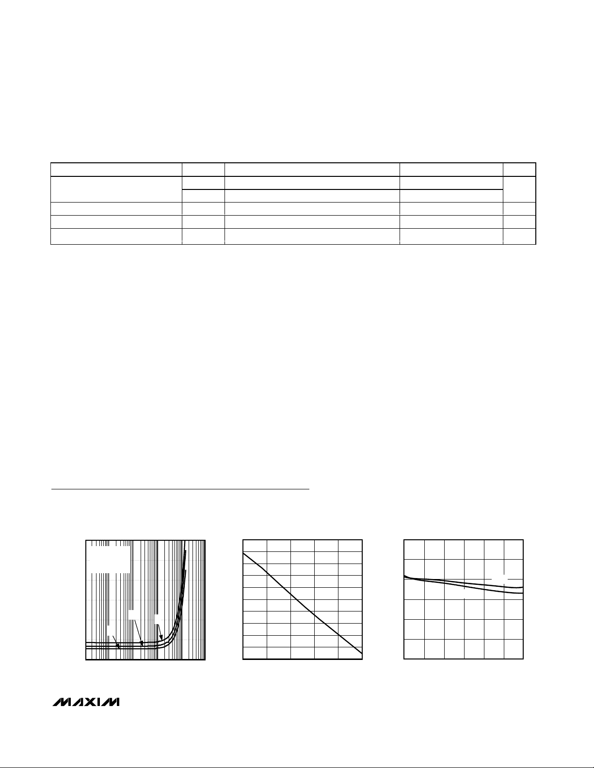
Typical Operating Characteristics
(VCC= +3.3V, RL = 100Ω, CL = 5pF, VIH= +3V, VIL= GND, fIN= 20MHz, TA= +25°C, unless otherwise noted.) (Figures 2, 3)
1 100 1M
MAX9110
SUPPLY CURRENT
vs. INPUT FREQUENCY
MAX9110 toc01
INPUT FREQUENCY (Hz)
SUPPLY CURRENT (mA)
9.5
6.5
7.0
7.5
8.0
8.5
9.0
10k
100M 1G
A: VCC = +3.0V
B: V
CC
= +3.3V
C: V
CC
= +3.6V
C
B
A
6.4
6.7
6.6
6.5
6.8
6.9
7.0
7.1
7.2
7.3
7.4
-40 10-15 356085
SUPPLY CURRENT vs. TEMPERATURE
MAX9110 toc02
TEMPERATURE (°C)
CURRENT SUPPLY (mA)
0.8
1.2
1.0
1.6
1.4
1.8
2.0
3.0 3.2 3.33.1 3.4 3.5 3.6
DIFFERENTIAL PROPAGATION DELAY
vs. SUPPLY VOLTAGE
MAX9110 toc03
SUPPLY VOLTAGE (V)
PROPAGATION DELAY (ns)
t
PLHD
t
PHLD
Part-to-Part Skew
High-to-Low Transition Time t
Low-to-High Transition Time t
Maximum Operating Frequency f
PARAMETER SYMBOL CONDITIONS MIN TYP MAX UNITS
t
SKD3
t
SKD4
THL
TLH
MAX
(Note 8) 1
(Note 9) 1.5
ns
0.25 0.6 1 ns
0.25 0.6 1 ns
(Note 10) 250 MHz
Page 4

MAX9110/MAX9112
Single/Dual LVDS Line Drivers with
Ultra-Low Pulse Skew in SOT23
4 _______________________________________________________________________________________
Typical Operating Characteristics (continued)
(VCC= +3.3V, RL = 100Ω, CL = 5pF, VIH= +3V, VIL= GND, fIN= 20MHz, TA= +25°C, unless otherwise noted.) (Figures 2, 3)
250
275
300
325
350
375
400
425
450
3.0 3.23.1 3.3 3.4 3.5 3.6
MAX9110 toc10
SUPPLY VOLTAGE (V)
DIFFERENTIAL OUTPUT VOLTAGE (mV)
DIFFERENTIAL OUTPUT VOLTAGE
vs. SUPPLY VOLTAGE
250
275
300
325
350
375
400
425
450
75.0 100.087.5 112.5 125.0 137.5 150.0
MAX9110 toc11
LOAD RESISTANCE (Ω)
DIFFERENTIAL OUTPUT VOLTAGE (mV)
DIFFERENTIAL OUTPUT VOLTAGE
vs. LOAD RESISTANCE
VCC = +3.3V
VCC = +3V
VCC = +3.6V
0.8
1.2
1.0
1.6
1.4
1.8
2.0
-40 10-15 356085
MAX9110 toc04
TEMPERATURE (°C)
PROPAGATION DELAY (ns)
DIFFERENTIAL PROPAGATION DELAY
vs. TEMPERATURE
t
PLHD
t
PHLD
0
20
60
40
80
100
3.0 3.23.1 3.3 3.4 3.5 3.6
MAX9110 toc05
SUPPLY VOLTAGE (V)
DIFFERENTIAL PULSE SKEW (ps)
DIFFERENTIAL PULSE SKEW
vs. SUPPLY VOLTAGE
0
20
60
40
80
100
-40 10-15 35 60 85
DIFFERENTIAL PULSE SKEW
vs. TEMPERATURE
MAX9110 toc06
TEMPERATURE (°C)
DIFFERENTIAL PULSE SKEW (ps)
300
350
400
450
500
550
600
650
700
3.0 3.23.1 3.3 3.4 3.5 3.6
TRANSITION TIME vs. SUPPLY VOLTAGE
MAX9110 toc07
SUPPLY VOLTAGE (V)
TRANSITION TIME (ps)
t
TLH
t
THL
400
460
440
420
480
500
520
540
560
580
600
-40 10-15 35 60 85
TRANSITION TIME vs. TEMPERATURE
MAX9110 toc08
TEMPERATURE (°C)
TRANSITION TIME (ps)
t
TLH
t
THL
1.00
1.15
1.10
1.05
1.20
1.25
1.30
1.35
1.40
1.45
1.50
3.0 3.23.1 3.3 3.4 3.5 3.6
OUTPUT VOLTAGE vs. SUPPLY VOLTAGE
MAX9110 toc09
SUPPLY VOLTAGE (V)
OUTPUT VOLTAGE (V)
OUTPUT LOW
OUTPUT HIGH
Page 5
MAX9110/MAX9112
Single/Dual LVDS Line Drivers with
Ultra-Low Pulse Skew in SOT23
_______________________________________________________________________________________ 5
Typical Operating Characteristics (continued)
(VCC= +3.3V, RL = 100Ω, CL = 5pF, VIH= +3V, VIL= GND, fIN= 20MHz, TA= +25°C, unless otherwise noted.) (Figures 2, 3)
Pin Description
Detailed Description
The MAX9110/MAX9112 single/dual LVDS transmitters
are intended for high-speed, point-to-point, low-power
applications. These devices accept CMOS/LVTTL
inputs with data rates exceeding 500Mbps. The
MAX9110/MAX9112 reduce power consumption and
EMI by translating these signals to a differential voltage
in the 250mV to 450mV range across a 100Ω load while
drawing only 9.4mA of supply current for the dualchannel MAX9112.
A current-steering approach induces less ground
bounce and no shoot-through current, enhancing noise
margin and system speed performance. The output
OUTPUT HIGH VOLTAGE
1.45
1.44
1.43
1.42
1.41
1.40
1.39
1.38
OUTPUT HIGH VOLTAGE (V)
1.37
1.36
1.35
75.0 100.087.5 112.5 125.0 137.5 150.0
vs. LOAD RESISTANCE
VCC = +3.6V
VCC = +3V
VCC = +3.3V
LOAD RESISTANCE (Ω)
MAX9110 toc12
PIN
MAX9110 MAX9112
SOT23 SO SOT23 SO
1.10
1.09
1.08
1.07
1.06
1.05
1.04
1.03
OUTPUT LOW VOLTAGE (V)
1.02
1.01
1.00
75.0 100.087.5 112.5 125.0 137.5 150.0
NAME FUNCTION
OUTPUT LOW VOLTAGE
vs. LOAD RESISTANCE
MAX9110 toc13
VCC = +3.6V
VCC = +3V
VCC = +3.3V
LOAD RESISTANCE (Ω)
4141VCCPositive Supply
1 2 — — DIN
Transmitter Input
— — 1, 3 2, 3 DIN1, DIN2
3, 5, 6 3, 5, 6 — — N.C. No Connection. Not internally connected.
2 4 2 4 GND Ground
7 7 — — DO+
Noninverting Transmitter Output
— — 6, 7 6, 7 DO2+, DO1+
8 8 — — DO-
Inverting Transmitter Output
— — 5, 8 5, 8 DO2-, DO1-
Page 6

MAX9110/MAX9112
Single/Dual LVDS Line Drivers with
Ultra-Low Pulse Skew in SOT23
6 _______________________________________________________________________________________
Figure 1. LVDS Transmitter VODand VOSTest Circuit
Figure 2. Transmitter Propagation Delay and Transition Time
Test Circuit
stage presents a symmetrical, high-impedance output,
reducing differential reflection and timing distortion. The
driver outputs are short circuit current limited and enter a
high-impedance state when the device is not powered.
LVDS Operation
The LVDS interface standard is a signaling method
intended for point-to-point communication over a controlled impedance medium as defined by the EIA/TIA644 LVDS standard. The LVDS standard uses a lower
voltage swing than other common communication standards, achieving higher data rates with reduced power
consumption while reducing EMI emissions and system
susceptibility to noise.
LVDS transmitters such as the MAX9110/MAX9112
convert CMOS/LVTTL signals to low-voltage differential
signals at rates in excess of 500Mbps. The MAX9110/
MAX9112 current-steering architecture requires a resistive load to terminate the signal and complete the trans-
mission loop. Because the device switches the direction of current flow and not voltage levels, the actual
output voltage swing is determined by the value of the
termination resistor at the input of an LVDS receiver.
Logic states are determined by the direction of current
flow through the termination resistor. With a typical
3.5mA output current, the MAX9110/MAX9112 produce
an output voltage of 350mV when driving a 100Ω load.
The steady-state-voltage peak-to-peak swing is twice
the differential voltage, or 700mV (typ).
Applications Information
Supply Bypassing
Bypass VCCwith high-frequency surface-mount ceramic
0.1µF and 0.001µF capacitors in parallel, as close to the
device as possible, with the smaller valued capacitor the
closest. For additional supply bypassing, place a 10µF
tantalum or ceramic capacitor at the point where power
enters the circuit board.
Figure 3. Transmitter Propagation Delay and Transition Time Waveforms
DO_+
C
L
V
GND
CC
DIN_
RL/2
R
L
/2
DO_-
V
V
OS
20%
1.5V
t
PLHD
DIN_
-
DO_
DO_+
V
DIFF
OS
V
OD
t
TLH
0V DIFFERENTIAL
80%
V
0
DIFF
GENERATOR
DIN_
50
Ω
C
L
R
L
3V
1.5V
0
t
PHLD
V
OH
0
V
OL
80%
= V
+ - V
-
DO_
DO_
0
20%
t
THL
DO_ +
DO_ -
Page 7

Differential Traces
Output trace characteristics affect the performance of
the MAX9110/MAX9112. Use controlled impedance
traces to match trace impedance to both transmission
medium impedance and termination resistor. Eliminate
reflections and ensure that noise couples as common
mode by running the differential traces close together.
Reduce skew by matching the electrical length of the
traces. Excessive skew can result in a degradation of
magnetic field cancellation.
Maintain the distance between the differential traces to
avoid discontinuities in impedance. Avoid 90° turns and
minimize the number of vias to further prevent impedance discontinuities.
Cables and Connectors
Transmission media should have a differential characteristic impedance of about 100Ω. Use cables and connectors that have matched impedance to minimize
impedance discontinuities.
Avoid the use of unbalanced cables, such as ribbon or
simple coaxial cable. Balanced cables, such as twisted
pair, offer superior signal quality and tend to generate
less EMI due to canceling effects. Balanced cables
tend to pick up noise as common mode, which is
rejected by the LVDS receiver.
Termination
Termination resistors should match the differential characteristic impedance of the transmission line. Because
the MAX9110/MAX9112 are current-steering devices,
an output voltage will not be generated without a termination resistor. Output voltage levels are dependent
upon the termination resistor value. Resistance values
may range between 75Ω and 150Ω.
Minimize the distance between the termination resistor
and receiver inputs. Use a single 1% to 2% surfacemount resistor across the receiver inputs.
Board Layout
For LVDS applications, a four-layer PC board that provides separate power, ground, LVDS signals, and input
signals is recommended. Isolate the input and LVDS signals from each other to prevent coupling. Separate the
input and LVDS signal planes with the power and ground
planes for best results.
MAX9110/MAX9112
Single/Dual LVDS Line Drivers with
Ultra-Low Pulse Skew in SOT23
_______________________________________________________________________________________ 7
MAX9110 TRANSISTOR COUNT: 765
MAX9112 TRANSISTOR COUNT: 765
PROCESS: CMOS
Chip Information
Typical Operating Circuit
+3.3V
RECEIVERDRIVER
MAX9111
MAX9113
0.001μF 0.1μF
OUT_
DIN_
+3.3V
MAX9110
MAX9112
0.001μF 0.1μF
RT = 100Ω
LVDS
Page 8
MAX9110/MAX9112
Single/Dual LVDS Line Drivers with
Ultra-Low Pulse Skew in SOT23
Maxim cannot assume responsibility for use of any circuitry other than circuitry entirely embodied in a Maxim product. No circuit patent licenses are
implied. Maxim reserves the right to change the circuitry and specifications without notice at any time.
8 _____________________Maxim Integrated Products, 120 San Gabriel Drive, Sunnyvale, CA 94086 408-737-7600
© 2000 Maxim Integrated Products Printed USA is a registered trademark of Maxim Integrated Products.
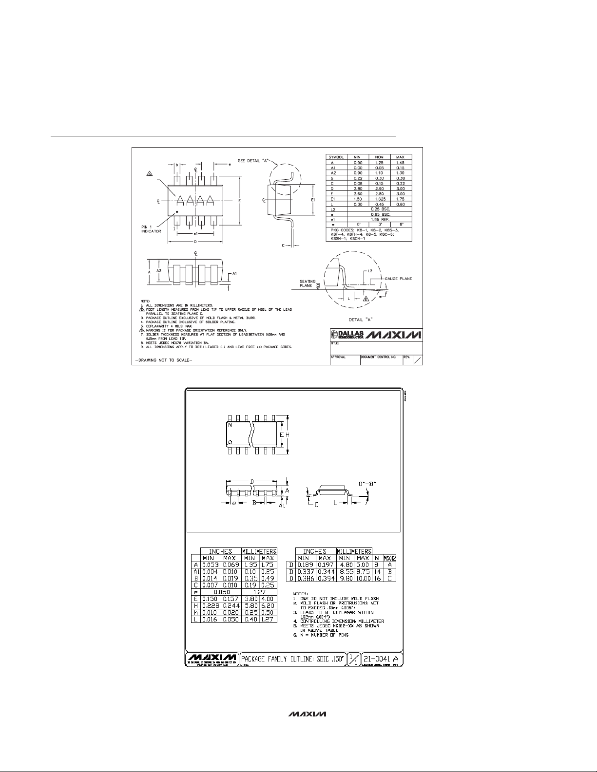
Package Information
MARKING
SOT23, 8L.EPS
0
0
PACKAGE OUTLINE, SOT-23, 8L BODY
21-0078 G
1
1
 Loading...