

Page 1
19-0129; Rev. 3; 7/94
Single/Dual/Quad High-Speed, Ultra Low-Power,
Single-Supply TTL Comparators
_______________General Description
The MAX907/MAX908/MAX909 dual, quad, and single
high-speed, ultra low-power voltage comparators are
designed for use in systems powered from a single
+5V supply; the MAX909 also accepts dual ±5V supplies. Their 40ns propagation delay (with 5mV input
overdrive) is achieved with a power consumption of
only 3.5mW per comparator. The wide input commonmode range extends from 200mV below ground (below
the negative supply rail for the MAX909) to within 1.5V
of the positive supply rail.
Because they are micropower, high-speed comparators that operate from a single +5V supply and include
built-in hysteresis, these devices replace a variety of
older comparators in a wide range of applications.
MAX907/MAX908/MAX909 outputs are TTL compatible, requiring no external pull-up circuitry. All inputs
and outputs can be continuously shorted to either supply rail without damage. These easy-to-use comparators incorporate internal hysteresis to ensure clean output switching even when the devices are driven by a
slow-moving input signal.
The MAX909 features complementary outputs and an
output latch. A separate supply pin for extending the
analog input range down to -5V is also provided.
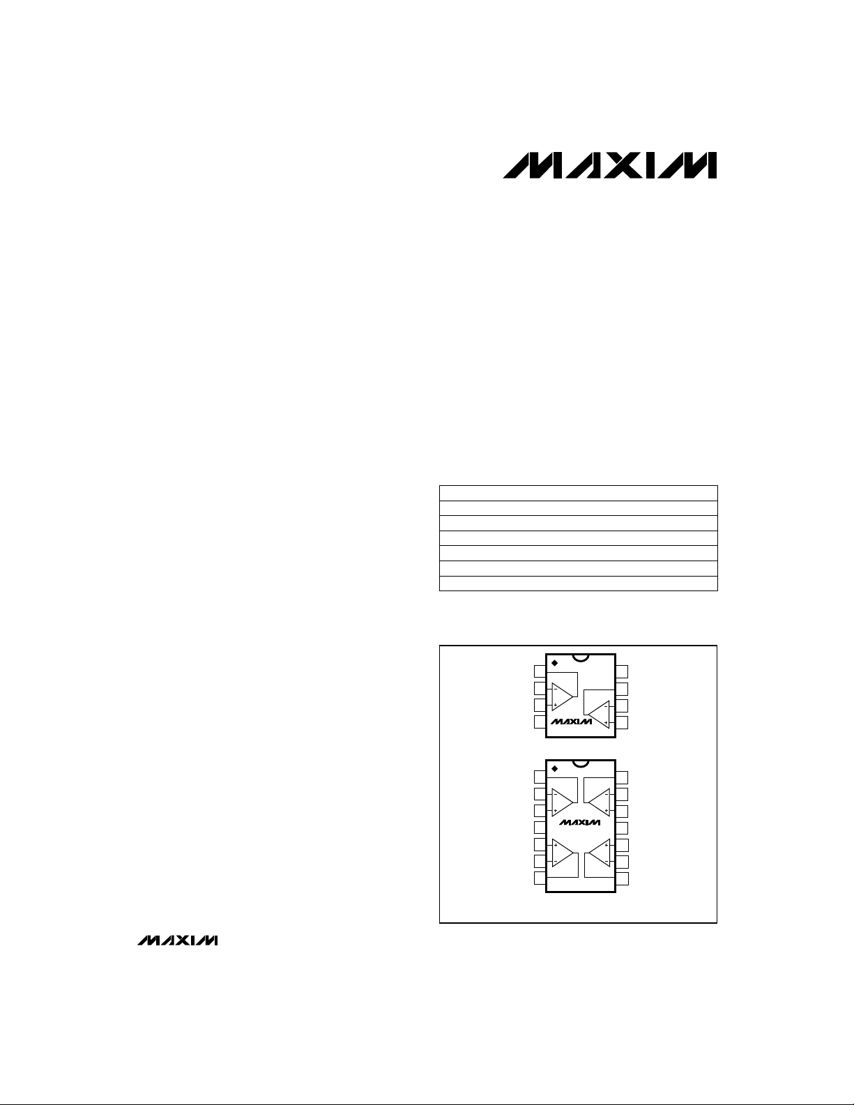
The dual MAX907 and single MAX909 are available in
8-pin DIP and small-outline packages, and the quad
MAX908 is available in 14-pin DIP and small-outline
packages. These comparators are ideal for single
+5V-supply applications that require the combination
of high speed, precision, and ultra-low power
dissipation.
_______________________Applications
Battery-Powered Systems
High-Speed A/D Converters
High-Speed V/F Converters
Line Receivers
Threshold Detectors/Discriminators
High-Speed Sampling Circuits
Zero Crossing Detectors
___________________________Features
♦ 40ns Propagation Delay
♦ 700µA (3.5mW) Supply Current per Comparator
♦ Single 4.5V to 5.5V Supply Operation
(or ±5V, MAX909 only)
♦ Wide Input Range Includes Ground
(or -5V, MAX909 only)
♦ Low, 500µV Offset Voltage
♦ Internal Hysteresis Provides Clean Switching
♦ TTL-Compatible Outputs
(Complementary on MAX909)
♦ Input and Output Short-Circuit Protection
♦ Internal Latch (MAX909 only)
______________Ordering Information
PART TEMP. RANGE PIN-PACKAGE
MAX907CPA
MAX907CSA 0°C to +70°C 8 SO
MAX907C/D 0°C to +70°C Dice*
MAX907EPA -40°C to +85°C 8 Plastic DIP
MAX907ESA -40°C to +85°C 8 SO
MAX907MJA -55°C to +125°C 8 CERDIP
Ordering Information continued on last page.
* Dice are specified at +25°C, DC parameters only.
0°C to +70°C 8 Plastic DIP
_________________Pin Configurations
TOP VIEW
Pin Configurations continued on last page.
OUTA
INAINA+
GND
OUTA
INAINA+
INB+
INB-
OUTB
1
2
3
4
MAX907
DIP/SO
1
2
3
4
V+
MAX908
5
6
7
DIP/SO
8
V+
OUTB
7
INB-
6
5
INB+
14
OUTD
IND-
13
IND+
12
11
GND
INC+
10
INC-
9
8
OUTC
MAX907/MAX908/MAX909
________________________________________________________________ Maxim Integrated Products
Call toll free 1-800-998-8800 for free samples or literature.
1
Page 2
Single/Dual/Quad High-Speed, Ultra Low-Power,
Single-Supply TTL Comparators
ABSOLUTE MAXIMUM RATINGS
Positive Supply Voltage (V+ to GND) ........................+7V
Negative Supply Voltage (V- to GND, MAX909 only).........-7V
Differential Input Voltage
MAX907/MAX908..........................-0.3V to (V+ + 0.3V)
MAX909 ..............................(V- - 0.3V) to (V+ + 0.3V)
Common-Mode Input Voltage
MAX907/MAX908..........................-0.3V to (V+ + 0.3V)
MAX909 ..............................(V- - 0.3V) to (V+ + 0.3V)
Latch Input Voltage (MAX909 only).........-0.3V to (V+ + 0.3V)
Input/Output Short-Circuit Duration to V+ or GND . ..Continuous
Continuous Power Dissipation (T
8-Pin Plastic DIP (derate 9.09mW/°C above +70°C)...727mW
8-Pin SO (derate 5.88mW/°C above +70°C) ...........471mW
8-Pin CERDIP (derate 8.00mW/°C above +70°C)......640mW
14-Pin Plastic DIP (derate 10.00mW/°C above +70°C) . ..800mW
14-Pin SO (derate 8.33mW/°C above +70°C)..........667mW
14-Pin CERDIP (derate 9.09mW/°C above +70°C) ....727mW
Operating Temperature Ranges:
MAX90_C_ _ ...................................... 0°C to +70°C
MAX90_E_ _ ...................................-40°C to +85°C
MAX90_MJ_ ..................................-55°C to +125°C
Storage Temperature Range ...................-65°C to +160°C
Lead Temperature (soldering, 10sec)....................+300°C
Stresses beyond those listed under “Absolute Maximum Ratings" may cause permanent damage to the device. These are stress ratings only, and functional
operation of the device at these or any other conditions beyond those indicated in the operational sections of the specifications is not implied. Exposure to
absolute maximum rating conditions for extended periods may affect device reliability.
ELECTRICAL CHARACTERISTICS
(V+ = 5V, TA= +25°C; MAX909 only: V- = 0V, V
MAX907/MAX908/MAX909
PARAMETER CONDITIONS MIN TYP MAX UNITS
Positive Trip Point
Negative Trip Point
Input Offset Voltage
Input Bias Current
Input Offset Current
Input Voltage Range
SYMBOL
V
TRIP+
V
TRIP-
V
OS
I
B
I
OS
V
CMR
Common-Mode Rejection Ratio CMRR (Notes 4, 5) 50 100 µV/V
Power-Supply Rejection Ratio PSRR (Notes 4, 6) 50 100 µV/V
Output High Voltage
Positive Supply Current per
Comparator
V
OH
V
OL
I+ (Note 7)
Negative Supply Current I- MAX909 only: V- = -5V 60 100 µA
Power Dissipation per
Comparator
Output Rise Time
Output Fall Time
PD (Note 8)
t
r
t
f
= 0V; unless otherwise noted.)
LATCH
(Note 1) 24 mV
(Note 1) -2 -4 mV
(Note 2) 0.5 2.0 mV
VCM= 0V, VIN= V
VCM= 0V, VIN= V
(Notes 3, 4)
I
SOURCE
I
= 3.2mA
SINK
I
= 8mA
SINK
OS
OS
MAX907/908/909
MAX909 only: V- = -5V
= 100µA
-0.2 V+ - 1.5
-5.2 V+ - 1.5
3.0 3.5
MAX907/MAX908
MAX909
MAX907/MAX908
MAX909
V
= 0.4V to 2.4V, CL= 10pF
OUT
V
= 2.4V to 0.4V, CL= 10pF
OUT
= +70°C)
A
100 300 nA
25 50 nA
0.3 0.4
0.4
0.7 1.0
1.2 1.8
3.5 5.5
610
12 ns
6 ns
V
V
VOutput Low Voltage
mA
mW
2 _______________________________________________________________________________________
Page 3
Single/Dual/Quad High-Speed, Ultra Low-Power,
Single-Supply TTL Comparators
ELECTRICAL CHARACTERISTICS (continued)
(V+ = 5V, TA= +25°C; MAX909 only: V- = 0V, V
PARAMETER
Propagation Delay
SYMBOL CONDITIONS MIN TYP MAX UNITS
t
PD+,tPD-
Differential Propagation Delay
Propagation Delay Skew
tPDskew
Latch Input Voltage High
Latch Input Voltage Low
Latch Input Current
IIH, I
Latch Setup Time
Latch Hold Time
ELECTRICAL CHARACTERISTICS
(V+ = 5V, TA= T
Positive Trip Point
Negative Trip Point
Input Offset Voltage
Input Bias Current
Input Offset Current
Input Voltage Range
Common-Mode Rejection Ratio CMRR (Notes 4, 5) 75 200 µV/V
Power-Supply Rejection Ratio PSRR (Notes 4, 6) 75 200 µV/V
Output High Voltage
Positive Supply Current per
Comparator
Negative Supply Current I- MAX909 only: V- = -5V 100 200 µA
Power Dissipation per Comparator PD (Note 8)
to T
MIN
MAX
PARAMETER
; MAX909 only: V- = 0V, V
SYMBOL CONDITIONS MIN TYP MAX UNITS
V
V
V
= 0V; unless otherwise noted.)
LATCH
VIN= 100mV, VOD= 5mV,
(Note 9)
∆t
VIN= 100mV, VOD= 5mV,
PD
(Note 10)
MAX909 only: VIN= 100mV,
= 5mV, (Note 11)
V
OD
V
V
TRIP+
TRIP-
V
I
I
(Note 12) 2.0 V
IH
(Note 12) 0.8 V
IL
(Note 12) 20 µA
IL
t
(Note 12) 2 ns
s
t
(Note 12) 2 ns
h
= 0V; unless otherwise noted.)
LATCH
(Note 1) 25 mV
(Note 1) -2 -5 mV
(Note 2) 13 mV
OS
VCM= 0V, VIN= V
B
VCM= 0V, VIN= V
OS
C/E temp.
ranges
(Notes 3, 4)
CMR
M temp.
range
(Notes 3, 4)
V
V
I
SOURCE
I
SINK
I
SINK
= 100µA
= 3.2mA
= 8mA
OH
OL
I+ (Note 7)
OS
OS
MAX909 only,
V- = -5V
MAX907/908/909
MAX909 only,
V- = -5V
MAX907/MAX908
MAX909
MAX907/MAX908
MAX909
40 50 ns
1 ns
2 ns
200 500 nA
50 100 nA
-0.2 V+ - 1.5MAX907/908/909
-5.2 V+ - 1.5
-0.1 V+ - 1.5
-5.1 V+ - 1.5
2.8 3.5
0.3 0.4
0.4
0.8 1.2
1.2 2.0
47
611
V
V
VOutput Low Voltage
mA
mW
MAX907/MAX908/MAX909
_______________________________________________________________________________________ 3
Page 4
Single/Dual/Quad High-Speed, Ultra Low-Power,
Single-Supply TTL Comparators
ELECTRICAL CHARACTERISTICS (continued)
(V+ = 5V, TA= T
Propagation Delay
Differential Propagation Delay
Propagation Delay Skew
Latch Input Voltage High
Latch Input Voltage Low
Latch Input Current
Latch Setup Time
Latch Hold Time
Note 1: Trip Point is defined as the input voltage required to make the comparator output change state. The difference
Note 2: Input Offset Voltage is defined as the center of the input-referred hysteresis zone. Specified for V
Note 3: Inferred from the CMRR test. Note that a correct logic result is obtained at the output, provided that at least one input is
MAX907/MAX908/MAX909
Note 4: Tested with V+ = 5.5V (and V- = 0V for MAX909). MAX909 also tested over the full analog input range (i.e., with
Note 5: Tested over the full input voltage range (V
Note 6: Specified over the full tolerance of operating supply voltage: MAX907/MAX908 tested with 4.5V < V+ < 5.5V. MAX909
Note 7: Positive Supply Current specified with the worst-case condition of all outputs at logic low (MAX907/MAX908), and
Note 8: Typical power specified with V+ = 5V; maximum with V+ = 5.5V (and with V- = -5.5V for MAX909).
Note 9: Due to difficulties in measuring propagation delay with 5mV of overdrive in automatic test equipment, the
Note 10: Differential Propagation Delay is specified as the difference between any two channels in the MAX907/MAX908 (both out-
Note 11: Propagation Delay Skew is specified as the difference between any single channel’s output low-to-high transition (t
Note 12: Latch specifications apply to MAX909 only. See Figure 2.
to T
MIN
PARAMETER
; MAX909 only: V- = 0V, V
MAX
SYMBOL CONDITIONS MIN TYP MAX UNITS
t
PD+,tPD-
∆t
PD
tPDskew
V
IH
V
IL
IIH, I
IL
t
s
t
h
between upper (V
+) and lower (V
TRIP
TRIP
Specified for an input common-mode voltage (V
within the V
limits. Note also that either or both inputs can be driven to the upper or lower absolute maximum limit with-
CMR
= 0V; unless otherwise noted.)
LATCH
VIN= 100mV, VOD= 5mV
(Note 9)
VIN= 100mV, VOD= 5mV
(Note 10)
MAX909 only: VIN= 100mV,
= 5mV (Note 11)
V
OD
45 70 ns
2 ns
4 ns
(Note 12) 2.0 V
(Note 12) 0.8 V
(Note 12) 20 µA
(Note 12) 4 ns
(Note 12) 4 ns
-) trip points is equal to the width of the input-referred hysteresis zone (V
) of 0V. See Figure 1.
CM
= 0V. See Figure 1.
CM
out damage to the part.
V- = -5.5V).
).
CMR
tested with 4.5V < V+ < 5.5V and with -5.5V < V- < 0V.
with V+ = 5.5V.
MAX907/MAX908/MAX909 are sample tested to 0.1% AQL with 100mV input overdrive. Correlation tests show that the
specification can be guaranteed if all other DC parameters are within the specified limits. V
must be added to the over-
OS
drive voltage for low values of overdrive.
puts making either a low-to-high or a high-to-low transition).
and high-to-low transition (t
-), and also between the QOUT and QOUT transition on the MAX909.
PD
HYST
).
+)
PD
4 _______________________________________________________________________________________
Page 5

Single/Dual/Quad High-Speed, Ultra Low-Power,
Single-Supply TTL Comparators
__________________________________________Typical Operating Characteristics
(V+ = 5V, TA= +25°C, unless otherwise noted.)
MAX907/MAX908/MAX909
PROPAGATION DELAY
50
40
30
20
PROPAGATION DELAY (ns)
10
70
60
50
40
PROPAGATION DELAY (ns)
30
2.0
1.5
(mA)
CC
1.0
TOTAL I
0.5
vs. INPUT OVERDRIVE
RS = 10Ω
= 15pF
C
LOAD
tPD+
tPD-
1 10 100
INPUT OVERDRIVE (mV)
PROPAGATION DELAY
vs. TEMPERATURE
VOD = 5mV
= 10Ω
R
S
= 15pF
C
LOAD
-60 -20 60 140
-40 0 8040 120
TOTAL POSITIVE SUPPLY CURRENT
20 100
TEMPERATURE (°C)
MAX907
vs. POSITIVE SUPPLY VOLTAGE
(OUTPUTS AT V
TA = +125°C
TA = +25°C
TA = -55°C
PROPAGATION DELAY
80
60
40
20
PROPAGATION DELAY (ns)
5.0
4.5
tPD+
t
-
PD
)
OL
(V)
4.0
OH
V
3.5
3.0
2.0
1.5
(mA)
CC
1.0
TOTAL I
0.5
vs. SOURCE IMPEDANCE
VOD = 5mV
= 15pF
C
LOAD
tPD+
tPD-
0
10 100 10k
SOURCE IMPEDANCE (Ω)
OUTPUT HIGH VOLTAGE
vs. SOURCE CURRENT
VIN = 100mV
TA = +125°C
TA = +25°C
TA = -55°C
1 10 1000
TOTAL POSITIVE SUPPLY CURRENT
vs. POSITIVE SUPPLY VOLTAGE
(OUTPUTS AT V
I
SOURCE
MAX907
TA = +125°C
TA = +25°C
TA = -55°C
(µA)
100
1k
)
OH
70
60
50
40
PROPAGATION DELAY (ns)
30
0.5
0.4
(V)
0.3
OL
V
0.2
0.1
4.0
3.0
(mA)
CC
2.0
TOTAL I
1.0
PROPAGATION DELAY
vs. CAPACITIVE LOAD
VOD = 5mV
= 10Ω
R
S
tPD+
tPD-
0 120
20 60 100
40
CAPACITIVE LOAD (pF)
OUTPUT LOW VOLTAGE
vs. SINK CURRENT
VIN = 100mV
TA = +25°C
TA = +125°C
012
2610
4
TOTAL POSITIVE SUPPLY CURRENT
vs. POSITIVE SUPPLY VOLTAGE
(OUTPUTS AT V
= -55°C
T
A
I
(mA)
SINK
MAX908
TA = +125°C
80
8
)
OL
TA = +25°C
TA = -55°C
0
28
357
4
6
V
(V)
CC
0
28
357
_________________________________________________________________________________________________
0
28
4
6
V
(V)
CC
357
4
6
V
(V)
CC
5
Page 6

Single/Dual/Quad High-Speed, Ultra Low-Power,
Single-Supply TTL Comparators
____________________________Typical Operating Characteristics (continued)
(V+ = 5V, TA= +25°C, unless otherwise noted.)
TOTAL POSITIVE SUPPLY CURRENT
4.0
3.0
(mA)
CC
2.0
TOTAL I
1.0
0
28
5
MAX907/MAX908/MAX909
4
0
INPUT VOLTAGE RANGE (V)
-1
-60 -20 60 140
-40 0 8040 120
MAX908
vs. POSITIVE SUPPLY VOLTAGE
(OUTPUTS AT V
TA = +125°C
357
4
INPUT VOLTAGE RANGE
vs. TEMPERATURE
20 100
TEMPERATURE (°C)
)
OH
TA = +25°C
TA = -55°C
6
V
(V)
CC
V
CMR+
V
CMR-
MAX909
POSITIVE SUPPLY CURRENT
vs. POSITIVE SUPPLY VOLTAGE
2.0
V- = -5V
1.0
TOTAL I+ (mA)
0
23 5 8
5
4
-5
INPUT VOLTAGE RANGE (V)
-6
-60 -20 60 140
46
MAX909
INPUT VOLTAGE RANGE
vs. TEMPERATURE
20 100
-40 40 120080
TEMPERATURE (°C)
V+ (V)
MAX909
NEGATIVE SUPPLY CURRENT
vs. NEGATIVE SUPPLY VOLTAGE
200
V+ = +5V
+125°C
+25°C
-55°C
7
V
+
CMR
V+ = +5V
V- = -5V
V
-
CMR
100
TOTAL I- (µA)
0
0-1 -3 -6
-2 -4
V- (V)
SHORT-CIRCUIT OUTPUT CURRENT
60
30
SHORT-CIRCUIT OUTPUT CURRENT (mA)
0
vs. TEMPERATURE
OUTPUT
SHORTED TO
V+ (SINKING)
-60 -20 60 140
20 100
-40 0 8040 120
TEMPERATURE (°C)
+125°C
+25°C
-55°C
-5 -7
OUTPUT
SHORTED TO
GND (SOURCING)
INPUT OFFSET VOLTAGE
0.5
(mV)
0
OS
V
-0.5
6
________________________________________________________________________________________________
vs. TEMPERATURE
V
= 1.4V
OUT
= 0V
V
CM
-60 -20 60 140
-40 0 8040 120
20 100
TEMPERATURE (°C)
300
200
INPUT CURRENT (nA)
100
INPUT BIAS CURRENT
vs. TEMPERATURE
VCM = 0V
= V
V
IN
OS
-60 -20 60 140
-40 0 8040 120
20 100
TEMPERATURE (°C)
4
VCM = 0V
2
(mV)
0
OS
V
-2
-4
-60 -20 60 140
-40 0 8040 120
TRIP POINT
vs. TEMPERATURE
V
TRIP+
V
TRIP-
20 100
TEMPERATURE (°C)
Page 7

Single/Dual/Quad High-Speed, Ultra Low-Power,
Single-Supply TTL Comparators
____________________________Typical Operating Characteristics (continued)
(V+ = 5V, TA= +25°C, unless otherwise noted.)
MAX907/MAX908/MAX909
INPUT
(20mV/div)
INPUT
(20mV/div)
OUTPUT
GND
PROPAGATION DELAY (t
PROPAGATION DELAY (t
MAX907/MAX908
(5mV OVERDRIVE)
tPD+
MAX909
(5mV OVERDRIVE)
tPD+
+)
PD
+)
PD
tPD SKEW
5mV OVERDRIVE
INPUT GND
OUTPUT
(500mV/div)
TTL
THRESHOLD (1.4V)
OUTPUT
GND
5mV OVERDRIVE
INPUT GND
QOUT
(1V/div)
1.4V
QOUT
RESPONSE TO 10MHz SINE WAVE
INPUT
(20mV/div)
INPUT
(20mV/div)
OUTPUT
GND
PROPAGATION DELAY (t
PROPAGATION DELAY (t
MAX907/MAX908
(5mV OVERDRIVE)
tPD-
MAX909
(5mV OVERDRIVE)
tPD- tPD SKEW
-)
PD
INPUT GND
-5mV OVERDRIVE
OUTPUT
(500mV/div)
TTL
THRESHOLD
(1.4V)
OUTPUT
GND
-)
PD
INPUT GND
-5mV OVERDRIVE
QOUT
(1V/div)
1.4V
QOUT
20mVp-p
10MHz SINE WAVE
INPUT
COMPARATOR
OUTPUT
(1V/div)
GND
TIME (50ns/div)
_________________________________________________________________________________________________
7
Page 8

Single/Dual/Quad High-Speed, Ultra Low-Power,
Single-Supply TTL Comparators
______________________________________________________________Pin Description
PIN
MAX907 MAX908 MAX909
1 1 OUTA Comparator A Output
2 2 INA- Comparator A Inverting Input
3 3 INA+ Comparator A Noninverting Input
8 4 1 V+ Positive Supply
5 5 INB+ Comparator B Noninverting Input
6 6 INB- Comparator B Inverting Input
7 7 OUTB Comparator B Output
8 OUTC Comparator C Output
9 INC- Comparator C Inverting Input
10 INC+ Comparator C Noninverting Input
4 11 6 GND Ground
12 IND+ Comparator D Noninverting Input
13 IND- Comparator D Inverting Input
14 OUTD Comparator D Output
2 IN+ Noninverting Input
3 IN- Inverting Input
MAX907/MAX908/MAX909
4 V- Negative Supply or Ground
5 LE
7 QOUT Comparator Output
8
NAME FUNCTION
The latch is transparent when LE is low. The comparator output is
stored when LE is high.
QOUT
Inverted Comparator Output
_______________Detailed Description
Timing
Noise or undesired parasitic AC feedback cause most
high-speed comparators to oscillate in the linear region
(i.e., when the voltage on one input is at or near the
voltage on the other input). The MAX907/MAX908/
MAX909 eliminate this problem by incorporating internal hysteresis. When the two comparator input voltages are equal, hysteresis effectively causes one comparator input voltage to move quickly past the other,
thus taking the input out of the region where oscillation
occurs. Standard comparators require that hysteresis
be added through the use of external resistors. The
MAX907/MAX908/MAX909’s fixed internal hysteresis
eliminates these resistors (and the equations required
to determine appropriate values).
8 _______________________________________________________________________________________
Adding hysteresis to a comparator creates two trip
points: one for the input voltage rising and one for the
input voltage falling (Figure 1). The difference between
these two input-referred trip points is the hysteresis.
Figure 1 illustrates the case where IN- is fixed and IN+
is varied. If the inputs were reversed, the figure would
look the same, except the output would be inverted.
The MAX909 includes an internal latch, allowing the
result of a comparison to be stored. If LE is low, the
latch is transparent (i.e., the comparator operates as
though the latch is not present). The state of the comparator output is stored when LE is high. See Figure 2.
Note that the MAX909 can be operated with V- connected to ground or to a negative supply voltage. The
MAX909’s input range extends from (V- - 0.2V) to
(V+ - 1.5V).
Page 9

Single/Dual/Quad High-Speed, Ultra Low-Power,
Single-Supply TTL Comparators
V
TRIP+
V
V
HYST
V
TRIP-
COMPARATOR
OUTPUT
IN+
V
+ V
TRIP+
V
=
OS
V
= 0V
IN-
V
V
TRIP-
2
OH
OL
Figure 1. Input and Output Waveforms, Noninverting Input
Varied
__________Applications Information
Circuit Layout
Because of the MAX907/MAX908/MAX909’s high gain
bandwidth, special precautions must be taken to realize the full high-speed capability. A printed circuit
board with a good, low-inductance ground plane is
mandatory. Place the decoupling capacitor (a 0.1µF
ceramic capacitor is a good choice) as close to V+ as
possible. Pay close attention to the decoupling capacitor’s bandwidth, keeping leads short. Short lead
lengths on the inputs and outputs are also essential to
avoid unwanted parasitic feedback around the comparators. Solder the device directly to the printed circuit board instead of using a socket.
Overdriving the Inputs
The inputs to the MAX907/MAX908/MAX909 may be
driven beyond the voltage limits given in the
Maximum Ratings
, as long as the current flowing into
the device is limited to 25mA. However, if the inputs
are overdriven, the output may be inverted. The addition of an external diode prevents this inversion by limiting the input voltage to 200mV to 300mV below ground
(see Figure 3).
Absolute
3V
LE
1.4V
COMPARE
0
V
INPUT
VOLTAGE
OUTPUT
(QOUT)
OUTPUT
Q
OUT)
(
V
1.4V
V
V
1.4V
V
OS
OH
OL
OH
OL
DIFFERENTIAL
Figure 2. MAX909 Timing Diagram
Battery-Operated Infrared Data Link
Figure 4's circuit allows reception of infrared data. The
MAX403 converts the photodiode current to a voltage,
and the MAX907 determines whether the amplifier output
is high enough to be called a “1”. The current consumption of this circuit is minimal: The MAX403 and MAX907
require typically 250µA and 700µA, respectively.
LATCH
t
h
t
s
V
OD
V
IN
tPD+
t
SKEW
MAX907/MAX908/MAX909
_______________________________________________________________________________________ 9
Page 10

Single/Dual/Quad High-Speed, Ultra Low-Power,
Single-Supply TTL Comparators
10pF
1M
V
= -200mV TO -300mV
I
CLAMP
SRC
V-
1/2 MAX907
MAX403
SIEMENS BP-104
PHOTODIODE
100k
1000pF
1000pF
+5V
7
4
100k
0.1µF
6
+5V
2
3
47k
+5V
3
2
0.1µF
8
1
DATA
4
MAX907
Figure 3. Schottky Clamp for Input Driven Below Ground
MAX907/MAX908/MAX909
Figure 4. Battery-Operated Infrared Data Link Consumes Only
1mA
10 ______________________________________________________________________________________
Page 11

Single/Dual/Quad High-Speed, Ultra Low-Power,
Single-Supply TTL Comparators
____Pin Configurations (continued) _Ordering Information (continued)
PART TEMP. RANGE PIN-PACKAGE
TOP VIEW
IN+
IN-
MAX908CPD
V+
1
MAX909
2
3
4
V-
DIP/SO
8
QOUT
QOUT
7
GND
6
5
LE
MAX908CSD 0°C to +70°C 14 SO
MAX908EPD -40°C to +85°C 14 Plastic DIP
MAX908ESD -40°C to +85°C 14 SO
MAX908MJD -55°C to +125°C 14 CERDIP
MAX909CPA
MAX909CSA 0°C to +70°C 8 SO
MAX909C/D 0°C to +70°C Dice*
MAX909EPA -40°C to +85°C 8 Plastic DIP
MAX909ESA -40°C to +85°C 8 SO
MAX909MJA -55°C to +125°C 8 CERDIP
* Dice are specified at +25°C, DC parameters only.
0°C to +70°C 14 Plastic DIP
0°C to +70°C 8 Plastic DIP
MAX907/MAX908/MAX909
______________________________________________________________________________________ 11
Page 12

Single/Dual/Quad High-Speed, Ultra Low-Power,
Single-Supply TTL Comparators
__________________________________________________________Chip Topographies
INB-
MAX907
INB+
MAX909
V+
OUTB
0.057"
V+
OUTA
INA-
INA+
0.055"
(1.40mm)
TRANSISTOR COUNT: MAX907:180
MAX908:360
MAX907/MAX908/MAX909
SUBSTRATE CONNECTED TO GND.
GND
(1.45mm)
IN+
IN-
V-
0.050"
(1.27mm)
TRANSISTOR COUNT: 95;
SUBSTRATE CONNECTED TO V-.
QOUT
QOUT
GND
LE
0.051"
(1.30mm)
Maxim cannot assume responsibility for use of any circuitry other than circuitry entirely embodied in a Maxim product. No circuit patent licenses are
implied. Maxim reserves the right to change the circuitry and specifications without notice at any time.
12
__________________Maxim Integrated Products, 120 San Gabriel Drive, Sunnyvale, CA 94086 (408) 737-7600
© 1994 Maxim Integrated Products Printed USA is a registered trademark of Maxim Integrated Products.
 Loading...