19-0129; Rev. 3; 7/94
Single/Dual/Quad High-Speed, Ultra Low-Power,
Single-Supply TTL Comparators
_______________General Description
The MAX907/MAX908/MAX909 dual, quad, and single
high-speed, ultra low-power voltage comparators are
designed for use in systems powered from a single
+5V supply; the MAX909 also accepts dual ±5V supplies. Their 40ns propagation delay (with 5mV input
overdrive) is achieved with a power consumption of
only 3.5mW per comparator. The wide input commonmode range extends from 200mV below ground (below
the negative supply rail for the MAX909) to within 1.5V
of the positive supply rail.
Because they are micropower, high-speed comparators that operate from a single +5V supply and include
built-in hysteresis, these devices replace a variety of
older comparators in a wide range of applications.
MAX907/MAX908/MAX909 outputs are TTL compatible, requiring no external pull-up circuitry. All inputs
and outputs can be continuously shorted to either supply rail without damage. These easy-to-use comparators incorporate internal hysteresis to ensure clean output switching even when the devices are driven by a
slow-moving input signal.
The MAX909 features complementary outputs and an
output latch. A separate supply pin for extending the
analog input range down to -5V is also provided.
The dual MAX907 and single MAX909 are available in
8-pin DIP and small-outline packages, and the quad
MAX908 is available in 14-pin DIP and small-outline
packages. These comparators are ideal for single
+5V-supply applications that require the combination
of high speed, precision, and ultra-low power
dissipation.
_______________________Applications
Battery-Powered Systems
High-Speed A/D Converters
High-Speed V/F Converters
Line Receivers
Threshold Detectors/Discriminators
High-Speed Sampling Circuits
Zero Crossing Detectors
___________________________Features
♦ 40ns Propagation Delay
♦ 700µA (3.5mW) Supply Current per Comparator
♦ Single 4.5V to 5.5V Supply Operation
(or ±5V, MAX909 only)
♦ Wide Input Range Includes Ground
(or -5V, MAX909 only)
♦ Low, 500µV Offset Voltage
♦ Internal Hysteresis Provides Clean Switching
♦ TTL-Compatible Outputs
(Complementary on MAX909)
♦ Input and Output Short-Circuit Protection
♦ Internal Latch (MAX909 only)
______________Ordering Information
PART TEMP. RANGE PIN-PACKAGE
MAX907CPA
MAX907CSA 0°C to +70°C 8 SO
MAX907C/D 0°C to +70°C Dice*
MAX907EPA -40°C to +85°C 8 Plastic DIP
MAX907ESA -40°C to +85°C 8 SO
MAX907MJA -55°C to +125°C 8 CERDIP
Ordering Information continued on last page.
* Dice are specified at +25°C, DC parameters only.
0°C to +70°C 8 Plastic DIP
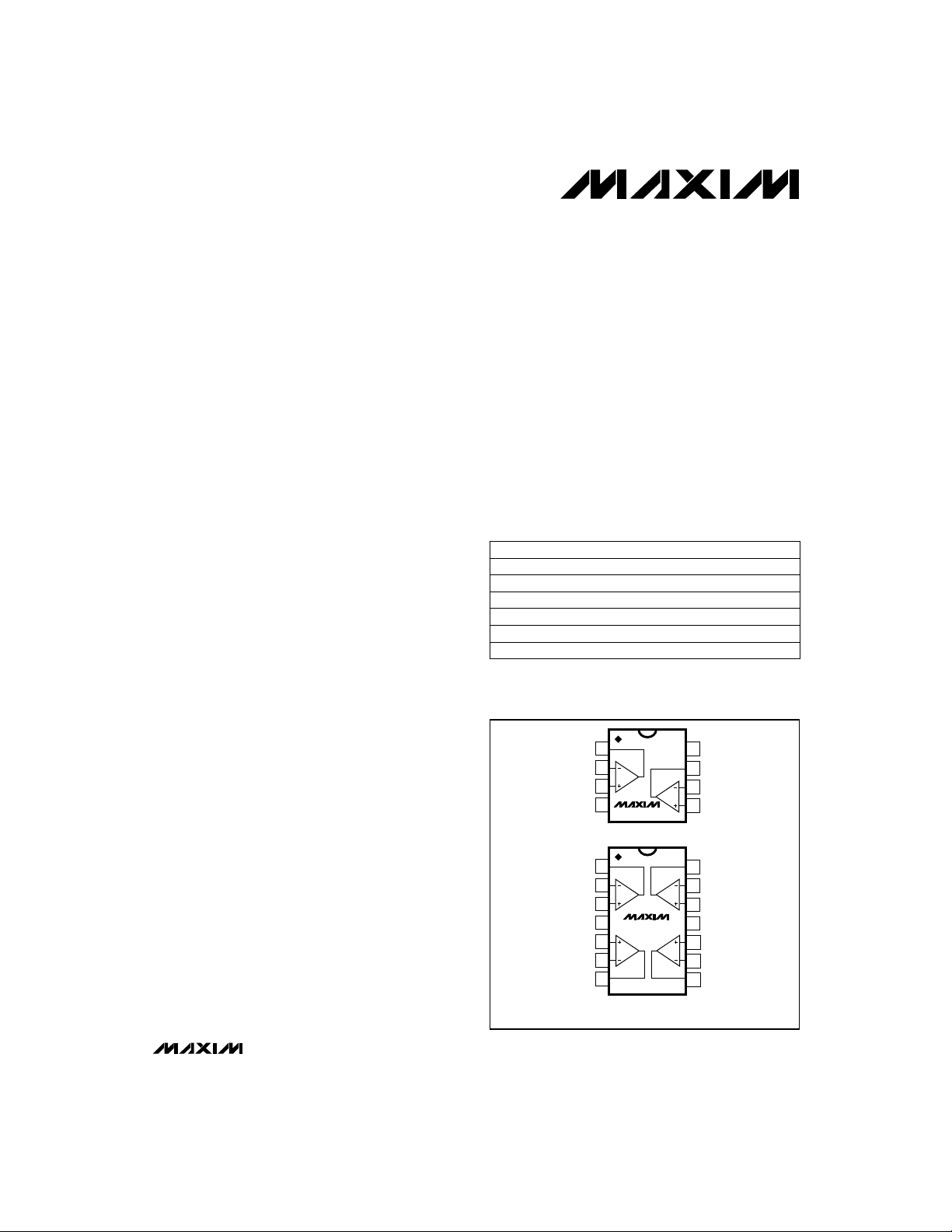
_________________Pin Configurations
TOP VIEW
Pin Configurations continued on last page.
OUTA
INAINA+
GND
OUTA
INAINA+
INB+
INB-
OUTB
1
2
3
4
MAX907
DIP/SO
1
2
3
4
V+
MAX908
5
6
7
DIP/SO
8
V+
OUTB
7
INB-
6
5
INB+
14
OUTD
IND-
13
IND+
12
11
GND
INC+
10
INC-
9
8
OUTC
MAX907/MAX908/MAX909
________________________________________________________________ Maxim Integrated Products
Call toll free 1-800-998-8800 for free samples or literature.
1

Single/Dual/Quad High-Speed, Ultra Low-Power,
Single-Supply TTL Comparators
ABSOLUTE MAXIMUM RATINGS
Positive Supply Voltage (V+ to GND) ........................+7V
Negative Supply Voltage (V- to GND, MAX909 only).........-7V
Differential Input Voltage
MAX907/MAX908..........................-0.3V to (V+ + 0.3V)
MAX909 ..............................(V- - 0.3V) to (V+ + 0.3V)
Common-Mode Input Voltage
MAX907/MAX908..........................-0.3V to (V+ + 0.3V)
MAX909 ..............................(V- - 0.3V) to (V+ + 0.3V)
Latch Input Voltage (MAX909 only).........-0.3V to (V+ + 0.3V)
Input/Output Short-Circuit Duration to V+ or GND . ..Continuous
Continuous Power Dissipation (T
8-Pin Plastic DIP (derate 9.09mW/°C above +70°C)...727mW
8-Pin SO (derate 5.88mW/°C above +70°C) ...........471mW
8-Pin CERDIP (derate 8.00mW/°C above +70°C)......640mW
14-Pin Plastic DIP (derate 10.00mW/°C above +70°C) . ..800mW
14-Pin SO (derate 8.33mW/°C above +70°C)..........667mW
14-Pin CERDIP (derate 9.09mW/°C above +70°C) ....727mW
Operating Temperature Ranges:
MAX90_C_ _ ...................................... 0°C to +70°C
MAX90_E_ _ ...................................-40°C to +85°C
MAX90_MJ_ ..................................-55°C to +125°C
Storage Temperature Range ...................-65°C to +160°C
Lead Temperature (soldering, 10sec)....................+300°C
Stresses beyond those listed under “Absolute Maximum Ratings" may cause permanent damage to the device. These are stress ratings only, and functional
operation of the device at these or any other conditions beyond those indicated in the operational sections of the specifications is not implied. Exposure to
absolute maximum rating conditions for extended periods may affect device reliability.
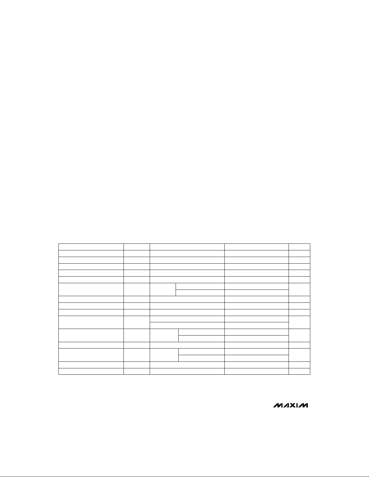
ELECTRICAL CHARACTERISTICS
(V+ = 5V, TA= +25°C; MAX909 only: V- = 0V, V
MAX907/MAX908/MAX909
PARAMETER CONDITIONS MIN TYP MAX UNITS
Positive Trip Point
Negative Trip Point
Input Offset Voltage
Input Bias Current
Input Offset Current
Input Voltage Range
SYMBOL
V
TRIP+
V
TRIP-
V
OS
I
B
I
OS
V
CMR
Common-Mode Rejection Ratio CMRR (Notes 4, 5) 50 100 µV/V
Power-Supply Rejection Ratio PSRR (Notes 4, 6) 50 100 µV/V
Output High Voltage
Positive Supply Current per
Comparator
V
OH
V
OL
I+ (Note 7)
Negative Supply Current I- MAX909 only: V- = -5V 60 100 µA
Power Dissipation per
Comparator
Output Rise Time
Output Fall Time
PD (Note 8)
t
r
t
f
= 0V; unless otherwise noted.)
LATCH
(Note 1) 24 mV
(Note 1) -2 -4 mV
(Note 2) 0.5 2.0 mV
VCM= 0V, VIN= V
VCM= 0V, VIN= V
(Notes 3, 4)
I
SOURCE
I
= 3.2mA
SINK
I
= 8mA
SINK
OS
OS
MAX907/908/909
MAX909 only: V- = -5V
= 100µA
-0.2 V+ - 1.5
-5.2 V+ - 1.5
3.0 3.5
MAX907/MAX908
MAX909
MAX907/MAX908
MAX909
V
= 0.4V to 2.4V, CL= 10pF
OUT
V
= 2.4V to 0.4V, CL= 10pF
OUT
= +70°C)
A
100 300 nA
25 50 nA
0.3 0.4
0.4
0.7 1.0
1.2 1.8
3.5 5.5
610
12 ns
6 ns
V
V
VOutput Low Voltage
mA
mW
2 _______________________________________________________________________________________

Single/Dual/Quad High-Speed, Ultra Low-Power,
Single-Supply TTL Comparators
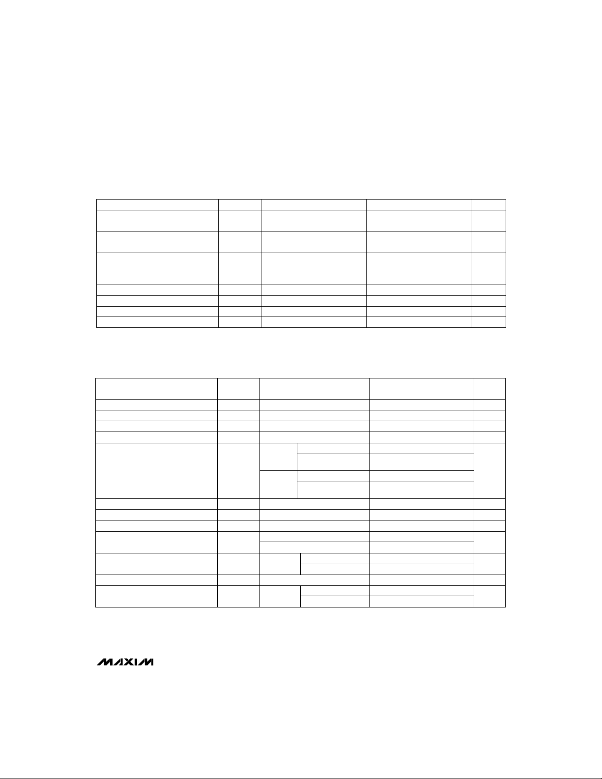
ELECTRICAL CHARACTERISTICS (continued)
(V+ = 5V, TA= +25°C; MAX909 only: V- = 0V, V
PARAMETER
Propagation Delay
SYMBOL CONDITIONS MIN TYP MAX UNITS
t
PD+,tPD-
Differential Propagation Delay
Propagation Delay Skew
tPDskew
Latch Input Voltage High
Latch Input Voltage Low
Latch Input Current
IIH, I
Latch Setup Time
Latch Hold Time
ELECTRICAL CHARACTERISTICS
(V+ = 5V, TA= T
Positive Trip Point
Negative Trip Point
Input Offset Voltage
Input Bias Current
Input Offset Current
Input Voltage Range
Common-Mode Rejection Ratio CMRR (Notes 4, 5) 75 200 µV/V
Power-Supply Rejection Ratio PSRR (Notes 4, 6) 75 200 µV/V
Output High Voltage
Positive Supply Current per
Comparator
Negative Supply Current I- MAX909 only: V- = -5V 100 200 µA
Power Dissipation per Comparator PD (Note 8)
to T
MIN
MAX
PARAMETER
; MAX909 only: V- = 0V, V
SYMBOL CONDITIONS MIN TYP MAX UNITS
V
V
V
= 0V; unless otherwise noted.)
LATCH
VIN= 100mV, VOD= 5mV,
(Note 9)
∆t
VIN= 100mV, VOD= 5mV,
PD
(Note 10)
MAX909 only: VIN= 100mV,
= 5mV, (Note 11)
V
OD
V
V
TRIP+
TRIP-
V
I
I
(Note 12) 2.0 V
IH
(Note 12) 0.8 V
IL
(Note 12) 20 µA
IL
t
(Note 12) 2 ns
s
t
(Note 12) 2 ns
h
= 0V; unless otherwise noted.)
LATCH
(Note 1) 25 mV
(Note 1) -2 -5 mV
(Note 2) 13 mV
OS
VCM= 0V, VIN= V
B
VCM= 0V, VIN= V
OS
C/E temp.
ranges
(Notes 3, 4)
CMR
M temp.
range
(Notes 3, 4)
V
V
I
SOURCE
I
SINK
I
SINK
= 100µA
= 3.2mA
= 8mA
OH
OL
I+ (Note 7)
OS
OS
MAX909 only,
V- = -5V
MAX907/908/909
MAX909 only,
V- = -5V
MAX907/MAX908
MAX909
MAX907/MAX908
MAX909
40 50 ns
1 ns
2 ns
200 500 nA
50 100 nA
-0.2 V+ - 1.5MAX907/908/909
-5.2 V+ - 1.5
-0.1 V+ - 1.5
-5.1 V+ - 1.5
2.8 3.5
0.3 0.4
0.4
0.8 1.2
1.2 2.0
47
611
V
V
VOutput Low Voltage
mA
mW
MAX907/MAX908/MAX909
_______________________________________________________________________________________ 3

Single/Dual/Quad High-Speed, Ultra Low-Power,
Single-Supply TTL Comparators
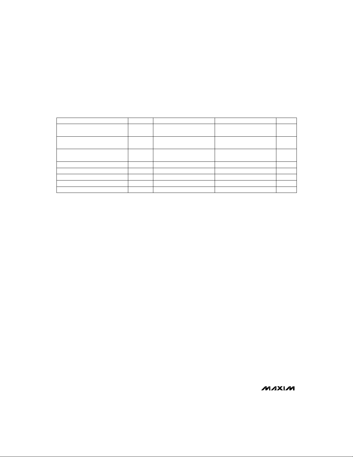
ELECTRICAL CHARACTERISTICS (continued)
(V+ = 5V, TA= T
Propagation Delay
Differential Propagation Delay
Propagation Delay Skew
Latch Input Voltage High
Latch Input Voltage Low
Latch Input Current
Latch Setup Time
Latch Hold Time
Note 1: Trip Point is defined as the input voltage required to make the comparator output change state. The difference
Note 2: Input Offset Voltage is defined as the center of the input-referred hysteresis zone. Specified for V
Note 3: Inferred from the CMRR test. Note that a correct logic result is obtained at the output, provided that at least one input is
MAX907/MAX908/MAX909
Note 4: Tested with V+ = 5.5V (and V- = 0V for MAX909). MAX909 also tested over the full analog input range (i.e., with
Note 5: Tested over the full input voltage range (V
Note 6: Specified over the full tolerance of operating supply voltage: MAX907/MAX908 tested with 4.5V < V+ < 5.5V. MAX909
Note 7: Positive Supply Current specified with the worst-case condition of all outputs at logic low (MAX907/MAX908), and
Note 8: Typical power specified with V+ = 5V; maximum with V+ = 5.5V (and with V- = -5.5V for MAX909).
Note 9: Due to difficulties in measuring propagation delay with 5mV of overdrive in automatic test equipment, the
Note 10: Differential Propagation Delay is specified as the difference between any two channels in the MAX907/MAX908 (both out-
Note 11: Propagation Delay Skew is specified as the difference between any single channel’s output low-to-high transition (t
Note 12: Latch specifications apply to MAX909 only. See Figure 2.
to T
MIN
PARAMETER
; MAX909 only: V- = 0V, V
MAX
SYMBOL CONDITIONS MIN TYP MAX UNITS
t
PD+,tPD-
∆t
PD
tPDskew
V
IH
V
IL
IIH, I
IL
t
s
t
h
between upper (V
+) and lower (V
TRIP
TRIP
Specified for an input common-mode voltage (V
within the V
limits. Note also that either or both inputs can be driven to the upper or lower absolute maximum limit with-
CMR
= 0V; unless otherwise noted.)
LATCH
VIN= 100mV, VOD= 5mV
(Note 9)
VIN= 100mV, VOD= 5mV
(Note 10)
MAX909 only: VIN= 100mV,
= 5mV (Note 11)
V
OD
45 70 ns
2 ns
4 ns
(Note 12) 2.0 V
(Note 12) 0.8 V
(Note 12) 20 µA
(Note 12) 4 ns
(Note 12) 4 ns
-) trip points is equal to the width of the input-referred hysteresis zone (V
) of 0V. See Figure 1.
CM
= 0V. See Figure 1.
CM
out damage to the part.
V- = -5.5V).
).
CMR
tested with 4.5V < V+ < 5.5V and with -5.5V < V- < 0V.
with V+ = 5.5V.
MAX907/MAX908/MAX909 are sample tested to 0.1% AQL with 100mV input overdrive. Correlation tests show that the
specification can be guaranteed if all other DC parameters are within the specified limits. V
must be added to the over-
OS
drive voltage for low values of overdrive.
puts making either a low-to-high or a high-to-low transition).
and high-to-low transition (t
-), and also between the QOUT and QOUT transition on the MAX909.
PD
HYST
).
+)
PD
4 _______________________________________________________________________________________
 Loading...