

Page 1
General Description
The MAX9065 is an ultra-small, low-power, window comparator ideal for a wide variety of portable electronics
applications such as cell phones, portable media players, and notebooks that have extremely tight board
space and power constraints. It comes in both a 4-bump
UCSP™ package with a 1mm x 1mm footprint (as small
as two 0402 resistors) and a 5-pin SOT23 package.
The MAX9065 features a common-mode input range of
-0.3V to +5.5V independent of supply voltage. The
input current goes to zero when the MAX9065 is powered down (VCC= 0). Additionally, the MAX9065 features high RF immunity.
The MAX9065 has a push-pull output and consumes
only 1µA (max) supply current. The MAX9065 operates
down to 1.0V over the extended -40°C to +85°C temperature range.
Applications
Cell Phones
Portable Media Players
Electronic Toys
Notebook Computers
Portable Medical Devices
Features
o Tiny 1mm x 1mm 4-Bump UCSP
Footprint = Two 0402 Resistors
Also Available in 5-Pin SOT23 Package
o Ultra-Low Power Operating Current
1µA (max)
o -0.3V to +5.5V Input Voltage Range
o 1.0V to 5.5V V
CC
Range
o 3.0V and 4.2V Trigger Points
o -40°C to +85°C Extended Temperature Range
MAX9065
Ultra-Small, Low-Power, Window Comparator
in 4 UCSP and 5 SOT23
________________________________________________________________
Maxim Integrated Products
1
19-4224; Rev 2; 1/11
For pricing, delivery, and ordering information, please contact Maxim Direct at 1-888-629-4642,
or visit Maxim’s website at www.maxim-ic.com.
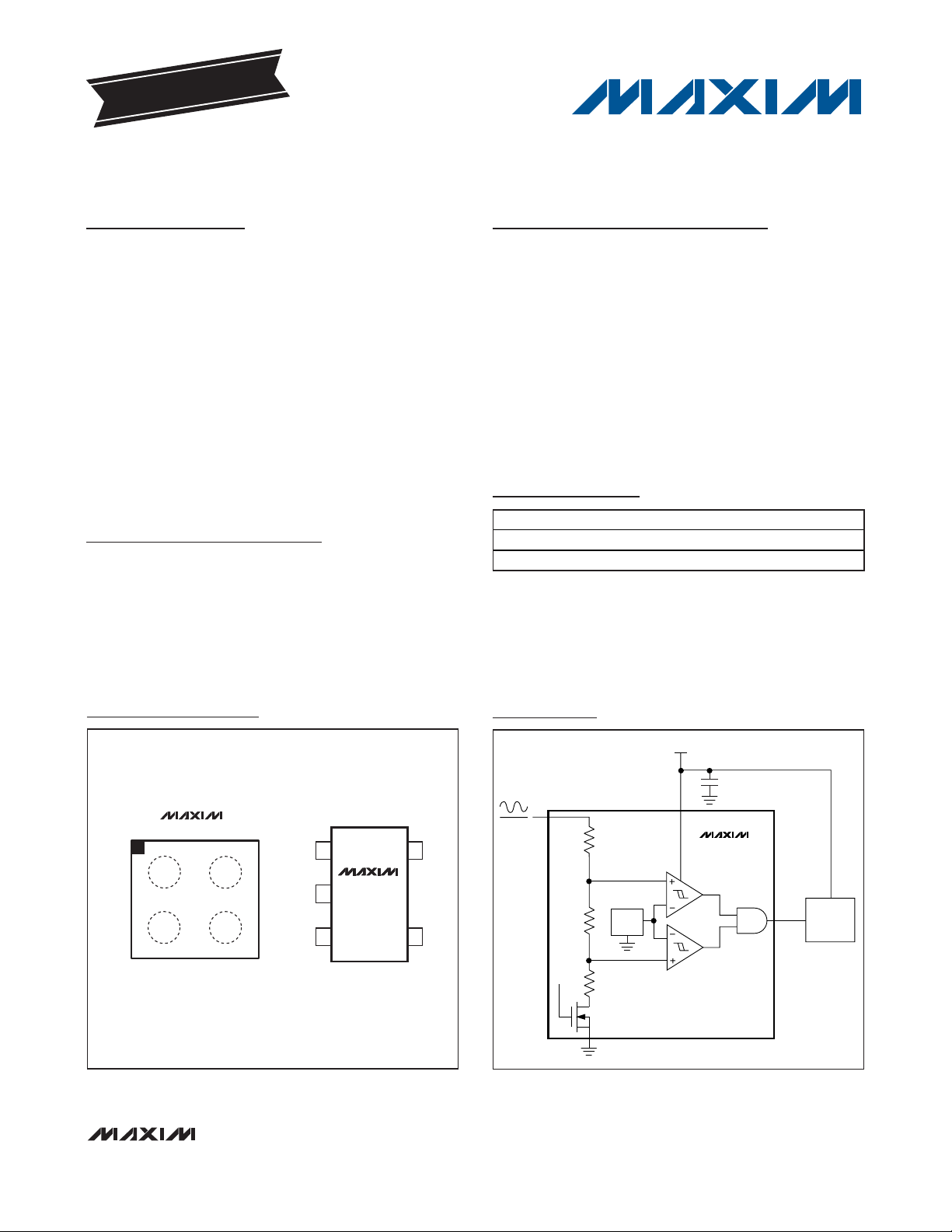
Pin Configurations
IN
1.0V TO 5.5V
MICRO
CONTROLLER
N
V
CC
V
LOWER
V
UPPER
OUT
V
CC
GND
0.1μF
I/O
V
DD
MAX9065
0.2V
REF
Typical Operating Circuit
Ordering Information
PART PIN-PACKAGE TOP MARK
MAX9065EBS+G45 4 UCSP AGC
MAX9065EUK+ 5 SOT23 AFFL
Note: All devices are specified over the extended -40°C to
+85°C operating temperature range.
+
Denotes a lead-free/RoHS-compliant package.
G45 = Protective die coating.
UCSP is a trademark of Maxim Integrated Products, Inc.
EVALUATION KIT
AVAILABLE
TOP VIEW
(BUMPS ON BOTTOM)
MAX9065
A1
B1
OUT
V
CC
A2
B2
UCSP
IN
GND
TOP VIEW
1 5 OUTVCC
2
GND
34
+
MAX9065
SOT23
INGND
Page 2
MAX9065
Ultra-Small, Low-Power, Window Comparator
in 4 UCSP and 5 SOT23
2 _______________________________________________________________________________________
ELECTRICAL CHARACTERISTICS
(VCC= 3.3V, TA= -40°C to +85°C. Typical values are at TA= +25°C, unless otherwise noted.) (Note 1)
Stresses beyond those listed under “Absolute Maximum Ratings” may cause permanent damage to the device. These are stress ratings only, and functional
operation of the device at these or any other conditions beyond those indicated in the operational sections of the specifications is not implied. Exposure to
absolute maximum rating conditions for extended periods may affect device reliability.
ABSOLUTE MAXIMUM RATINGS
VCC, IN to GND..........................................…………-0.3V to +6V
OUT to GND.................................…………-0.3V to (V
CC
+ 0.3V)
Output Short-Circuit Current Duration ....................................10s
Input Current into Any Terminal .......................................±20mA
Continuous Power Dissipation
4-Bump UCSP (derate 3.0mW/°C above +70°C)..........238mW
5-Pin SOT23 (derate 3.9mW/°C above +70°C).............312mW
Operating Temperature Range ..........................-40°C to +85°C
Junction Temperature .....................................................+150°C
Storage Temperature Range ............................-65°C to +150°C
Lead Temperature (SOT23 only, soldering 10s)..............+300°C
Soldering Temperature (reflow) .......................................+260°C
DC CHARACTERISTICS
Upper Threshold Voltage UTV
Lower Threshold Voltage LTV
Input Voltage Range V
Hysteresis V
Resistor String Input Resistance R
Input Shutdown Current I
Output Voltage Low V
Output Voltage High V
AC CHARACTERISTICS
Propagation Delay t
Fall Time t
Rise Time t
POWER SUPPLY
Supply Voltage V
PARAMETER SYMBOL CONDITIONS MIN TYP MAX UNITS
MAX9065EBS+
4 UCSP
MAX9065EUK+
5 SOT23
MAX9065EBS+
4 UCSP
MAX9065EUK+
5 SOT23
IN
HYS
IN_SHDNVCC
OH
PD
CC
(Note 2) ±1.0 %
IN
= 0V, VIN = 5.5V 1 15 nA
I
= 100µA, VCC = 1V, TA = +25°C 0.2
SINK
I
OL
F
R
= 1.2mA, VCC = 3.3V 0.3
SINK
I
= 1.2mA, VCC = 5.5V 0.5
SINK
I
I
I
Overdrive = ±100mV (Notes 3, 4) 25 µs
CL = 10pF 14 ns
CL = 10pF 30 ns
Guaranteed by VOS tests 1 5.5 V
= 25µA, VCC = 1V, TA = +25°C
SOURCE
= 0.3mA, VCC = 3.3V
SOURCE
= 0.75mA, VCC = 5.5V
SOURCE
TA = +25°C 4.158 4.20 4.242
-40°C < T
TA = +25°C 4.04 4.20 4.36
-40°C < T
TA = +25°C 2.94 3.00 3.06
-40°C < T
TA = +25°C 2.88 3.00 3.12
-40°C < T
< +85°C 4.10 4.30
A
< +85°C 3.98 4.42
A
< +85°C 2.92 3.08
A
< +85°C 2.83 3.17
A
-0.3 +5.5 V
5.8 11 17.7 MΩ
V
-
CC
0.2
V
-
CC
0.3
V
-
CC
0.5
V
V
V
V
Page 3
MAX9065
Ultra-Small, Low-Power, Window Comparator
in 4 UCSP and 5 SOT23
_______________________________________________________________________________________
3
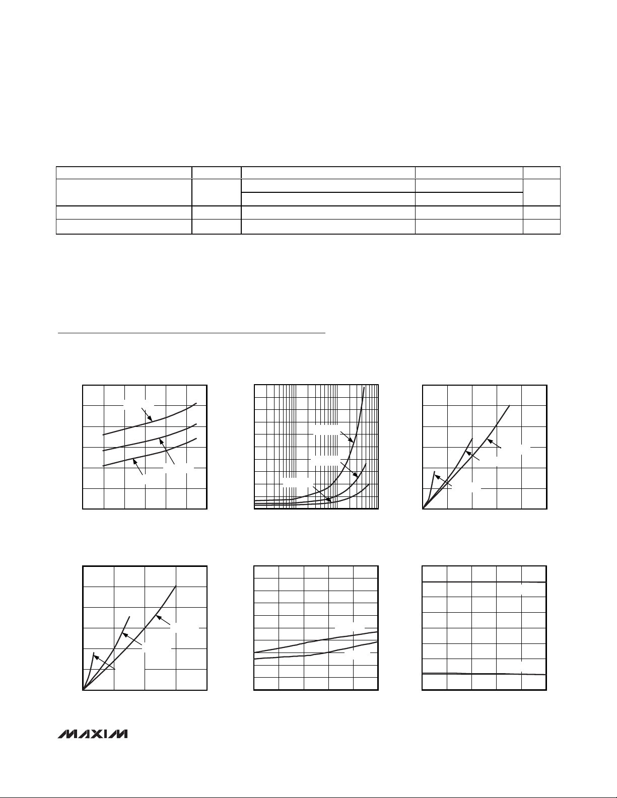
Typical Operating Characteristics
(VCC= 3.3V, TA= -40°C to +85°C. Typical values are at TA= +25°C, unless otherwise noted.)
ELECTRICAL CHARACTERISTICS (continued)
(VCC= 3.3V, TA= -40°C to +85°C. Typical values are at TA= +25°C, unless otherwise noted.) (Note 1)
Note 1: All devices are 100% production tested at T
A
= +25°C. Temperature limits are guaranteed by design.
Note 2: Hysteresis is the input voltage difference between the two switching points.
Note 3: Overdrive is defined as the voltage above or below the average of the switching points.
Note 4: Guaranteed by ATE and/or bench characterization over temperature.
Supply Current I
Power-Supply Rejection Ratio PSRR VCC = 0.9V to 5.5V, TA = +25°C 40 53 dB
Power-Up Time t
PARAMETER SYMBOL CONDITIONS MIN TYP MAX UNITS
CC
ON
VCC = 5.5V 0.7 1.35
VCC = 1.0V, TA = +25°C 0.6 1.0
3ms
SUPPLY CURRENT
vs. SUPPLY VOLTAGE
1200
1000
800
600
400
SUPPLY CURRENT (nA)
200
0
0231 456
TA = +85°C
TA = +25°C
TA = -40°C
SUPPLY VOLTAGE (V)
MAX9065 toc01
vs. OUTPUT TRANSITION FREQUENCY
SUPPLY CURRENT
50
45
40
35
30
25
20
15
SUPPLY CURRENT (µA)
10
5
0
0.1 100
VCC = 1.8V
OUTPUT TRANSITION FREQUENCY (kHz)
VCC = 5V
VCC = 3.3V
101
3.0
2.5
MAX9065 toc02
2.0
1.5
1.0
OUTPUT VOLTAGE LOW (V)
0.5
0
OUTPUT VOLTAGE LOW
vs. SINK CURRENT
VCC = 5V
VCC = 3.3V
VCC = 1.8V
084121620
SINK CURRENT (mA)
µA
MAX9065 toc03
OUTPUT VOLTAGE HIGH
vs. SOURCE CURRENT
3.0
2.5
2.0
1.5
1.0
OUTPUT VOLTAGE HIGH (V)
0.5
0
04268
VCC = 1.8V
SOURCE CURRENT (mA)
VCC = 5V
VCC = 3.3V
MAX9065 toc04
HYSTERESIS VOLTAGE
vs. TEMPERATURE
100
90
80
70
60
50
40
HYSTERESIS (mV)
30
20
10
0
-40 10-15 35 60 85
TEMPERATURE (°C)
VTH = 4.2V
VTH = 3V
4.4
4.2
MAX9065 toc05
4.0
3.8
3.6
3.4
THRESHOLD VOLTAGE (V)
3.2
3.0
2.8
-40 -15 10 35 60 85
THRESHOLD VOLTAGE
vs. TEMPERATURE
VTH = 4.2V
TEMPERATURE (°C)
MAX9065 toc06
VTH = 3V
Page 4

MAX9065
Ultra-Small, Low-Power, Window Comparator
in 4 UCSP and 5 SOT23
4 _______________________________________________________________________________________
Typical Operating Characteristics (continued)
(VCC= 3.3V, TA= -40°C to +85°C. Typical values are at TA= +25°C, unless otherwise noted.)
0
5
15
10
20
25
021 3456
PROPAGATION DELAY
vs. SUPPLY VOLTAGE
MAX9065 toc10
SUPPLY VOLTAGE (V)
PROPAGATION DELAY (ms)
VTH = 4.2V
VTH = 3V
VOD = ±200mV
200µs/div
1kHz FREQUENCY RESPONSE
IN
200mV/div
OUT
2V/div
MAX9065 toc11
VCC = 3.3V
4.4V
4V
0V
20µs/div
10kHz FREQUENCY RESPONSE
IN
200mV/div
OUT
2V/div
MAX9065 toc12
VCC = 3.3V
4.4V
4V
0V
1ms/div
OUTPUT RESPONSE TO SUPPLY
VOLTAGE TRANSIENT
V
CC
200mV/div
OUT
2V/div
OUT
2V/div
OUT
2V/div
MAX9065 toc13
VIN = VTH + 50mV
VIN = VTH + 150mV
VIN = VTH + 300mV
3.2V
3V
0V
0V
0V
1ms/div
POWER-UP/POWER-DOWN RESPONSE
V
CC
2V/div
OUT
2V/div
MAX9065 toc14
VIN = 4.3V
V
CC
= 3.3V
0V
0V
POWER-SUPPLY REJECTION
FOR NO FALSE TRIGGERING
MAX9065 toc15
FREQUENCY (Hz)
TRIP POINT (V)
100k10k1k100
4.08
4.10
4.12
4.14
4.16
4.18
4.20
4.22
4.24
4.26
4.28
4.30
4.32
4.34
4.06
10 1M
UPPER TRIP POINT
LOWER TRIP POINT
VCC = 3.3V + 100mV
P-P
2.4
2.8
2.6
3.2
3.0
3.6
3.4
3.8
4.2
4.0
4.4
1.0 2.0 2.5 3.01.5 3.5 4.0 4.5 5.55.0 6.0
THRESHOLD VOLTAGE
vs. SUPPLY VOLTAGE
MAX9065 toc07
SUPPLY VOLTAGE (V)
THRESHOLD VOLTAGE (V)
VTH = 4.2V
VTH = 3V
7
11
9
17
15
13
23
21
19
25
-40 10-15 356085
PROPAGATION DELAY
vs. TEMPERATURE
MAX9065 toc08
TEMPERATURE (°C)
PROPAGATION DELAY (µs)
VCC = 5V
VCC = 3.3V
VCC = 1.8V
0
50
100
150
200
250
08010040 6020 120 140 160 180 200
PROPAGATION DELAY
vs. INPUT OVERDRIVE
MAX9065 toc09
INPUT OVERDRIVE (mV)
PROPAGATION DELAY (µs)
VCC = 1.8V
VCC = 3.3V
VCC = 5V
VTH = 4.2V
Page 5

Detailed Description
The MAX9065 is an extremely small window comparator designed for compact, low-current applications, featuring a supply current of less than 1µA (max).
Operation
At the heart of the MAX9065 are two comparators, a
resistor-divider with a disconnect switch, a 200mV reference, digital logic circuitry, and an output stage (see
the
Typical Operating Circuit
).
The digital logic circuitry and the output stage together
behave like an AND gate. The gate’s inputs are the outputs of the two comparators. When either comparator’s
output is low, the output asserts low. When both comparator’s outputs are high, the output asserts high.
When power is applied to VCC, the n-channel FET at
the bottom of the resistor-divider is turned on. The
resistor-divider provides two voltages, V
UPPER
and
V
LOWER
, for comparison with an internal 0.2V reference
voltage. When the input voltage exceeds 4.2V, V
UPPER
is greater than 0.2V, causing the output to assert low.
When the input voltage falls below 3.0V, V
LOWER
is less
than 0.2V, causing the output also to assert low. With
the input voltage between 3.0V and 4.2V, the output
asserts high, indicating that the input voltage is within
the desired range. Table 1 summarizes the operation of
the MAX9065.
When V
CC
goes to 0V, the n-channel FET is turned off,
eliminating the resistor-divider as a leakage path for
current.
Applications
The MAX9065 is designed specifically to monitor the
voltage on a single lithium battery. Keeping the voltage
on a lithium battery within a tight range is important to
prevent damage to the battery. Specifically, ensuring
that the battery’s voltage neither exceeds 4.2V nor falls
below 3.0V lengthens the lifetime of the battery and
avoids any hazardous battery conditions.
Hysteresis
There are four trip points for hysteresis. See Figure 1.
Power-Supply Considerations
Bypass VCCwith a 0.1µF capacitor to ground.
Chip Information
PROCESS: BiCMOS
MAX9065
Ultra-Small, Low-Power, Window Comparator
in 4 UCSP and 5 SOT23
_______________________________________________________________________________________ 5
Pin Description
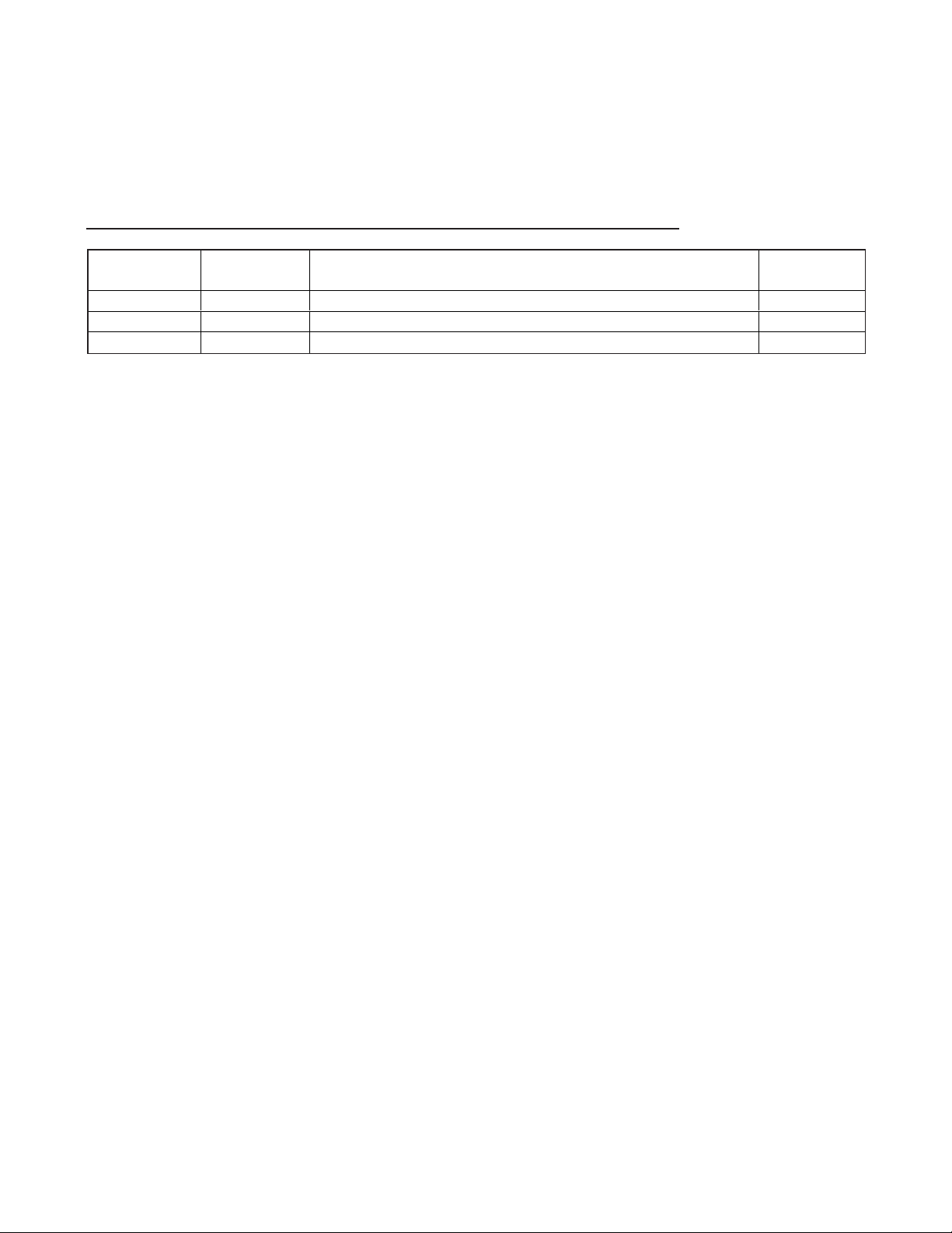
Table 1. MAX9065 Operation
PIN
SOT23 UCSP
1B1V
2, 3 B2 GND Ground
4 A2 IN Window Comparator Input
5 A1 OUT Push-Pull Output
NAME FUNCTION
External Supply Input. Bypass
to ground with a 0.1µF bypass
CC
capacitor.
INPUT VOLTAGE OUTPUT
VIN > 4.2V Low
3.0V < V
< 4.2V High
IN
VIN < 3.0V Low
Page 6

MAX9065
Ultra-Small, Low-Power, Window Comparator
in 4 UCSP and 5 SOT23
6 _______________________________________________________________________________________
Figure 1. Hysteresis Trip Points
UTV = 4.2V
HYSTERESIS = 1%
IN
HYSTERESIS = 1%
LTV = 3.0V
OUT
Page 7

MAX9065
Ultra-Small, Low-Power, Window Comparator
in 4 UCSP and 5 SOT23
_______________________________________________________________________________________ 7
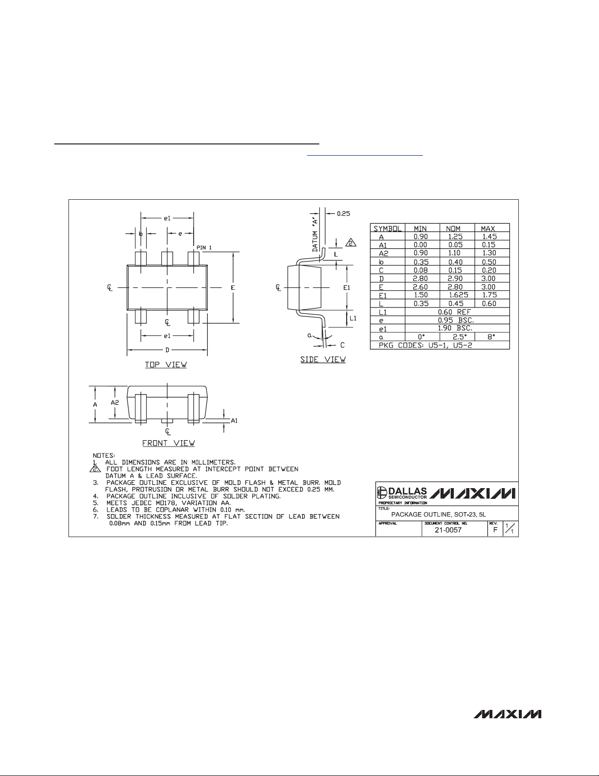
Package Information
For the latest package outline information and land patterns, go to www.maxim-ic.com/packages. Note that a “+”, “#”, or “-” in the
package code indicates RoHS status only. Package drawings may show a different suffix character, but the drawing pertains to the
package regardless of RoHS status.
PACKAGE TYPE PACKAGE CODE OUTLINE NO.
LAND
PATTERN NO.
5 SOT23 U5+2
21-0057
90-0174
4 UCSP B4+1
21-0117
Refer to Application Note 1891
Page 8
MAX9065
Ultra-Small, Low-Power, Window Comparator
in 4 UCSP and 5 SOT23
8 _______________________________________________________________________________________
Package Information (continued)
For the latest package outline information and land patterns, go to www.maxim-ic.com/packages. Note that a "+", "#", or "-" in the
package code indicates RoHS status only. Package drawings may show a different suffix character, but the drawing pertains to the
package regardless of RoHS status.
SOT-23 5L .EPS
Page 9
MAX9065
Ultra-Small, Low-Power, Window Comparator
in 4 UCSP and 5 SOT23
Maxim cannot assume responsibility for use of any circuitry other than circuitry entirely embodied in a Maxim product. No circuit patent licenses are
implied. Maxim reserves the right to change the circuitry and specifications without notice at any time.
Maxim Integrated Products, 120 San Gabriel Drive, Sunnyvale, CA 94086 408-737-7600 _____________________
9
© 2011 Maxim Integrated Products Maxim is a registered trademark of Maxim Integrated Products, Inc.
Revision History
REVISION
NUMBER
0 7/08 Initial release —
1 10/08 Removed future part reference from 5 SOT23 package 1
2 1/11 Added G45 designation 1
REVISION
DATE
DESCRIPTION
PAGES
CHANGED
 Loading...