

Page 1
General Description
The MAX9060–MAX9064 are small single comparators,
ideal for a wide variety of portable electronics applications such as cell phones, media players, and notebooks
that have extremely tight board space and power constraints. These comparators are offered in both, a miniature 4-bump UCSP™ package with a 1mm x 1mm
footprint (as small as two 0402 resistors), and a 5-pin
SOT23 package.
The MAX9060–MAX9064 feature an input voltage range
of -0.3V to +5.5V independent of supply voltage. These
devices maintain high impedance at the inputs even
when powered down (VCCor V
REF
= 0V). They also
feature internal filtering to provide high RF immunity.
The MAX9060 and MAX9061 have open-drain outputs
and draw quiescent supply current from a user-supplied
reference voltage, V
REF
, between 0.9V and 5.5V. These
devices consume only 100nA (max) supply current and
operate over the extended -40°C to +85°C temperature
range.
The MAX9062, MAX9063 and MAX9064 are single comparators with an internal 0.2V reference. These devices
feature either a push-pull or an open-drain output. They
consume only 700nA (max) supply current. The MAX9062,
MAX9063, and MAX9064 operate down to VCC= 1V
over the extended -40°C to +85°C temperature range.
Applications
Cell Phones
Portable Media Players
Electronic Toys
Notebook Computers
Portable Medical Devices
Features
o Tiny 1mm x 1mm x 0.6mm 4-Bump UCSP
Footprint = Two 0402 Resistors
Also Available in a 5-Pin SOT23 Package
o Ultra-Low Operating Current (100nA max)
o Input Voltage Range = -0.3V to +5.5V
o External REF Range = 0.9V to 5.5V
(MAX9060/MAX9061)
o Internal REF Voltage = 0.2V
(MAX9062/MAX9063/MAX9064)
o 15µs Propagation Delay
o -40°C to +85°C Extended Temperature Range
MAX9060–MAX9064
Ultra-Small, Low-Power Single
Comparators in 4-Bump UCSP and 5 SOT23
________________________________________________________________
Maxim Integrated Products
1
Pin Configuration
19-4105; Rev 4; 3/11
For pricing, delivery, and ordering information, please contact Maxim Direct at 1-888-629-4642,
or visit Maxim’s website at www.maxim-ic.com.
EVALUATION KIT
AVAILABLE
Ordering Information
PART PIN-PACKAGE TOP MARK
MAX9060EBS+G45
4 UCSP AFX
MAX9060EUK+ 5 SOT23 AFFG
MAX9061EBS+G45
4 UCSP AFY
MAX9061EUK+ 5 SOT23 AFFH
MAX9062EBS+G45
4 UCSP AFZ
MAX9062EUK+ 5 SOT23 AFFI
MAX9063EBS+G45
4 UCSP AGA
MAX9063EUK+ 5 SOT23 AFFJ
MAX9064EBS+G45
4 UCSP AGB
MAX9064EUK+ 5 SOT23 AFFK
Note: All devices are specified over the extended -40°C to
+85°C operating temperature range.
+
Denotes a lead(Pb)-free/RoHS-compliant package.
G45 = Protective die coating.
UCSP is a trademark of Maxim Integrated Products, Inc.
Selector Guide and Typical Operating Circuits appear at
end of data sheet.
TOP VIEW (BUMPS ON BOTTOM)
OUT
A1
(V
MAX9060–MAX9064
REF
B1 B2INGND
)
CC
+
REF
1
)
(V
A2
UCSP SOT23
REF = MAX9060/MAX9061
) = MAX9062–MAX9064
(V
CC
CC
GND
GND
MAX9060–
2
MAX9064
3
5
OUT
IN
4
Page 2
MAX9060–MAX9064
Ultra-Small, Low-Power Single
Comparators in 4-Bump UCSP and 5 SOT23
2 _______________________________________________________________________________________
ABSOLUTE MAXIMUM RATINGS
MAX9060/MAX9061 ELECTRICAL CHARACTERISTICS
(V
REF
= 1.8V, R
PULLUP
= 10kΩ to V
PULLUP
= 3.3V, TA = -40°C to +85°C. Typical values are at TA= +25°C, unless otherwise noted.)
(Note 1)
Stresses beyond those listed under “Absolute Maximum Ratings” may cause permanent damage to the device. These are stress ratings only, and functional
operation of the device at these or any other conditions beyond those indicated in the operational sections of the specifications is not implied. Exposure to
absolute maximum rating conditions for extended periods may affect device reliability.
VCC, REF, IN to GND................................................-0.3V to +6V
OUT to GND (MAX9060–MAX9063).........................-0.3V to +6V
OUT to GND (MAX9064 Only) ................-0.3V to + (V
CC
+ 0.3V)
Output Short-Circuit Current Duration ....................................10s
Input Current into Any Terminal........................................±20mA
Continuous Power Dissipation
4-Bump UCSP (derate 3.0mW/°C above +70°C) .......238 mW
5-Pin SOT23 (derate 3.9mW/°C above +70°C)...........312 mW
Operating Temperature Range ...........................-40°C to +85°C
Junction Temperature......................................................+150°C
Storage Temperature Range .............................-65°C to +150°C
Lead Temperature (excluding UCSP, soldering, 10s).....+300°C
Soldering Temperature (reflow) .......................................+260°C
PARAMETER SYMBOL CONDITIONS MIN TYP MAX UNITS
DC CHARACTERISTICS
Input Offset Voltage
(Note 2)
Hysteresis V
Input Voltage Range V
Input Bias Current I
Input Shutdown Current I
Output Voltage Low V
Output Leakage Current
(OUT = High)
AC CHARACTERISTICS
Propagation Delay t
Fall Time t
REF SUPPLY
REF Voltage V
REF Input Current I
REF Rejection Ratio RRR V
Power-Up Time t
V
OS
HYS
IN
IN
IN_PD
OL
I
OUT_LEAKAGEVPULLUP
PD
F
REF
REF
ON
TA = +25°C 1.3 6
(Note 3) ±12 mV
0V < VIN < V
V
REF
V
REF
I
SINK
T
= +25°C
A
I
SINK
I
SINK
I
SINK
REF
+ 0.6V < VIN < 5.5V 10 100
= 0V, VIN = 5.5V (Note 4) < 0.1 27 nA
= 25µA, V
= 200µA, V
= 500µA, V
= 1.2mA, V
= 5.5V (Note 4) < 0.1 35 nA
Overdrive = ±100mV (Note 5) 25 µs
CL = 10pF 14 ns
Guaranteed by VOS tests 0.9 5.5 V
V
= 0.9V, VIN = V
REF
= +25°C
T
A
V
= 1.8V, VIN = V
REF
= +25°C
T
A
V
= 5.5V, VIN = V
REF
= +25°C
T
A
V
= 5.5V, VIN = V
REF
-40°C < T
REF
< +85°C
A
= 0.9V to 5.5V, TA = +25°C 63 90 dB
-0.3 +5.5 V
+ 0.6V 40
= 0.9V,
REF
= 1.2V 0.08 0.20
REF
= 1.8V 0.13 0.23
REF
= 5.5V 0.19 0.50
REF
,
REF
,
REF
,
REF
,
REF
0.04 0.20
50 100
60
170 320
350
3ms
9
mV
nA
V
nA
Page 3
MAX9060–MAX9064
Ultra-Small, Low-Power Single
Comparators in 4-Bump UCSP and 5 SOT23
_______________________________________________________________________________________ 3
Note 1: All devices are 100% production tested at TA = +25°C. Temperature limits are guaranteed by design.
Note 2: Guaranteed by ATE and/or bench characterization over temperature. V
OS
is the average of the trip points minus V
REF
.
Note 3: Hysteresis is half the input voltage difference between the two switching points.
Note 4: Too small to be measured in an ATE test environment. Only gross test to catch failures is implemented.
Note 5: Overdrive is defined as the voltage above or below the switching points.
Note 6: Guaranteed by ATE and/or bench characterization over temperature. V
REF
is the average of the trip points.
Note 7: Includes reference error along with comparator offset voltage error.
MAX9062/MAX9063/MAX9064 ELECTRICAL CHARACTERISTICS
(VCC= 3.3V, R
PULLUP
= 10kΩ to V
PULLUP
= 3.3V for MAX9062/MAX9063, TA= -40°C to +85°C. Typical values at TA= +25°C, unless
otherwise noted.) (Note 1)
PARAMETER SYMBOL CONDITIONS MIN TYP MAX UNITS
DC CHARACTERISTICS
Input Voltage Range V
Input Bias Current I
Input Leakage Current I
Output Voltage Low V
Output Voltage High
(MAX9064 Only)
Output Leakage Current
(MAX9062/MAX9063 Only)
AC CHARACTERISTICS
Propagation Delay t
Fall Time t
Rise Time t
REFERENCE VOLTAGE
Input Threshold (Note 6) V
I
OUT_LEAKAGE
IN
IN
IN_SHDN
OL
V
OH
PD
F
R
REF
Guaranteed by IIN test -0.3 +5.5 V
VIN = 0.2V to 5.5V (Note 4) 0.06 15 nA
VCC = 0V, VIN = 5.5V (Note 4) < 0.1 15 nA
I
= 50µA, VCC = 1.0V 0.03 0.2
SINK
I
= 200µA, VCC = 1.2V 0.08 0.20
SINK
I
= 500µA, VCC = 1.8V 0.13 0.23
SINK
I
= 0.75mA, VCC = 3.3V 0.14 0.3
SINK
I
= 1.2mA, VCC = 5.5V 0.19 0.5
SINK
I
I
I
I
I
OUT = high, V
(Note 4)
V
= 15µA, VCC = 1.0V V
SOURCE
= 40µA, VCC = 1.2V V
SOURCE
= 180µA, VCC = 1.8V V
SOURCE
= 0.3mA, VCC = 3.3V V
SOURCE
= 0.75mA, VCC = 5.5V V
SOURCE
= 5.5V
PULLUP
OVERDRIVE
= ±100mV (Note 5) 15 µs
- 0.08V V
C C
- 0.08V V
C C
- 0.15V V
C C
- 0.13V V
C C
- 0.24V V
C C
C C
C C
C C
C C
C C
< 0.1 15 nA
CL = 10pF 14 ns
CL = 10pF, MAX9064 only 30 ns
TA = +25°C 188 200 212
TA = -40°C to +85°C 185 200 215
- 0.2V
- 0.20V
- 0.23V
- 0.3V
- 0.5V
V
V
mV
Input Threshold Hysteresis V
REF Tempco V
REF_TEMPCO
Power-Supply Rejection
Ratio
HYS
PSRR V
TA = -40°C to +85°C (Note 3) ±0.9 mV
(Note 7) 6 µV/°C
= 1.0V to 5.5V 40 53 dB
CC
POWER SUPPLY
Supply Voltage V
Supply Current I
Power-Up Time t
CC
CC
ON
Guaranteed by V
tests 1.0 5.5 V
OL/VOH
VCC = 1.0V 0.4 0.7
VCC = 5.5V 0.6 1.1
3ms
µA
Page 4
MAX9060–MAX9064
Ultra-Small, Low-Power Single
Comparators in 4-Bump UCSP and 5 SOT23
4 _______________________________________________________________________________________
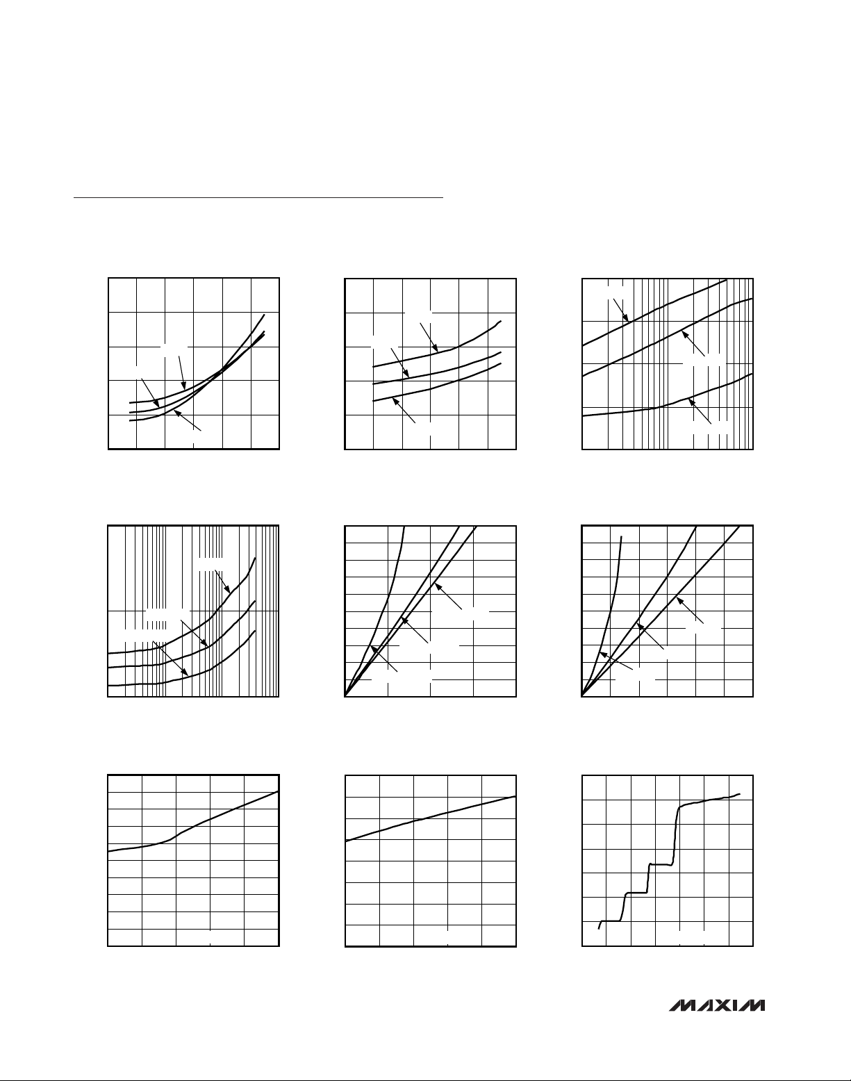
Typical Operating Characteristics
(VCC= 3.3V, V
REF
= 1.8V, R
PULLUP
= 10kΩ to V
PULLUP
= 3.3V for MAX9060–MAX9063, V
GND
= 0V, TA= +25°C, unless otherwise noted.)
MAX9060 SUPPLY CURRENT
vs. REF VOLTAGE
MAX9060 toc01
REF VOLTAGE (V)
SUPPLY CURRENT (nA)
54321
50
100
150
200
250
0
06
+85°C
-40°C
+25°C
MAX9064 SUPPLY CURRENT
vs. SUPPLY VOLTAGE
MAX9060 toc02
SUPPLY VOLTAGE (V)
SUPPLY CURRENT (nA)
54321
200
400
600
800
1000
0
06
+85°C
-40°C
+25°C
MAX9060 SUPPLY CURRENT
vs. OUTPUT TRANSITION FREQUENCY
MAX9060 toc03
OUTPUT TRANSITION FREQUENCY (kHz)
SUPPLY CURRENT (µA)
1
0.1
1
10
100
0.01
0.1 10
V
REF
= 5V
V
REF
= 3.3V
V
REF
= 1.8V
MAX9064 SUPPLY CURRENT
vs. OUTPUT TRANSITION FREQUENCY
MAX9060 toc04
OUTPUT TRANSITION FREQUENCY (kHz)
SUPPLY CURRENT (µA)
110
10
100
1
0.1 100
V
CC
= 5V
V
CC
= 3.3V
V
CC
= 1.8V
MAX9060 AND MAX9064 OUTPUT
VOLTAGE LOW vs. SINK CURRENT
MAX9060 toc05
SINK CURRENT (mA)
OUTPUT VOLTAGE LOW (V)
62
0.5
1.0
0.1
0.6
0.4
0.9
0.3
0.8
0.2
0.7
0
048
VCC/V
REF
= 3.3V
VCC/V
REF
= 1.8V
VCC/V
REF
= 5V
MAX9064 OUTPUT VOLTAGE HIGH
vs. SOURCE CURRENT
MAX9060 toc06
SOURCE CURRENT (mA)
OIUTPUT VOLTAGE HIGH (V
CC
- V
OH
, V)
0.5
1.0
0.1
0.6
0.4
0.9
0.3
0.8
0.2
0.7
0
0 1.51.0 2.5 3.00.5 2.0
VCC = 3.3V
VCC = 1.8V
VCC = 5V
MAX9060 OFFSET VOLTAGE
vs. TEMPERATURE
MAX9060 toc07
TEMPERATURE (°C)
OFFSET VOLTAGE (mV)
0.5
1.0
0.1
0.6
0.4
0.9
0.3
0.8
0.2
0.7
0
-40 6035-15 8510
V
REF
= 1.8V
MAX9060 HYSTERESIS VOLTAGE
vs. TEMPERATURE
MAX9060 toc08
TEMPERATURE (°C)
HYSTERESIS VOLTAGE (mV)
10
16
2
12
8
6
4
14
0
-40 6035-15 8510
V
REF
= 1.8V
MAX9060 INPUT BIAS CURRENT
vs. INPUT BIAS VOLTAGE
MAX9060 toc09
INPUT BIAS VOLTAGE (V)
INPUT BIAS CURRENT (nA)
20
30
0
25
15
10
5
-5
-1 1036425
V
REF
= 1.8V
Page 5

MAX9060–MAX9064
Ultra-Small, Low-Power Single
Comparators in 4-Bump UCSP and 5 SOT23
_______________________________________________________________________________________ 5
Typical Operating Characteristics (continued)
(VCC= 3.3V, V
REF
= 1.8V, R
PULLUP
= 10kΩ to V
PULLUP
= 3.3V for MAX9060–MAX9063, V
GND
= 0V, TA= +25°C, unless otherwise noted.)
MAX9060 PROPAGATION DELAY
AT V
REF
= 1.8V
MAX9060 toc16
100µs/div
0V
1.7V
1.9V
IN+
100mV/div
OUT
2V/div
MAX9064 PROPAGATION DELAY
AT V
CC
= 3.3V
MAX9060 toc17
100µs/div
0V
0.1V
0.3V
IN+
100mV/div
OUT
2V/div
MAX9064 INPUT BIAS CURRENT
vs. INPUT BIAS VOLTAGE
5
0
-5
-10
INPUT BIAS CURRENT (nA)
-15
-20
0 0.20 0.25 0.300.05 0.10 0.15
INPUT BIAS VOLTAGE (V)
MAX9064 PROPAGATION DELAY
vs. TEMPERATURE
17
16
15
14
13
12
PROPAGATION DELAY (µs)
11
10
9
-40 -15 60 853510
VCC = 3.3V
VOD = ±100mV
TEMPERATURE (°C)
VCC = 5V
VCC = 3.3V
VCC = 1.8V
MAX9060 toc10
MAX9060 toc13
MAX9064 REFERENCE VOLTAGE
vs. TEMPERATURE
202.0
201.9
201.8
201.7
201.6
201.5
201.4
201.3
REFERENCE VOLTAGE (mV)
201.2
201.1
201.0
-40 8510 60-15 35
TEMPERATURE (°C)
MAX9064 PROPAGATION DELAY
vs. INPUT OVERDRIVE
80
70
60
50
VCC = 1.8V
40
VCC = 3.3V
INPUT OVERDRIVE (mV)
PROPAGATION DELAY (µs)
30
20
10
0
0 100 150 25020050
VCC = 3.3V
VCC = 5V
MAX9064 REFERENCE VOLTAGE
vs. SUPPLY VOLTAGE
201.0
200.8
MAX9060 toc11
200.6
200.4
200.2
200.0
199.8
199.6
REFERENCE VOLTAGE (mV)
199.4
199.2
199.0
1.0 5.02.5 3.0 4.54.01.5 2.0 3.5
SUPPLY VOLTAGE (V)
MAX9060 PROPAGATION DELAY
vs. INPUT OVERDRIVE
80
PROPAGATION DELAY (µs)
70
60
50
40
30
20
10
0
0 100 150 25020050
V
= 1.8V
REF
V
= 5V
REF
INPUT OVERDRIVE (mV)
MAX9060 toc14
MAX9060 toc12
MAX9060 toc15
Page 6

MAX9060–MAX9064
Ultra-Small, Low-Power Single
Comparators in 4-Bump UCSP and 5 SOT23
6 _______________________________________________________________________________________
Typical Operating Characteristics (continued)
(VCC= 3.3V, V
REF
= 1.8V, R
PULLUP
= 10kΩ to V
PULLUP
= 3.3V for MAX9060–MAX9063, V
GND
= 0V, TA= +25°C, unless otherwise noted.)
MAX9064 OUTPUT RESPONSE
TO SUPPLY VOLTAGE TRANSIENT
MAX9060 toc22
1ms/div
0V
0V
0V
3V
3.2V
V
CC
200mV/div
OUT
2V/div
OUT
2V/div
OUT
2V/div
VIN = VTH + 20mV
VIN = VTH + 10mV
VIN = VTH + 1mV
MAX9064 POWER-SUPPLY REJECTION
FOR NO FALSE TRIGGERING
MAX9060 toc23
FREQUENCY (Hz)
TRIP POINT (mV)
100k100
200
206
194
202
196
204
198
10 10k1k 1M
VCC = 3.3V + 100mV
P-P
UPPER TRIP POINT
LOWER TRIP POINT
MAX9060 1kHz FREQUENCY RESPONSE
MAX9060 toc19
200µs/div
0V
1.7V
1.9V
1.8V
IN+
100mV/div
OUT
2V/div
V
REF
= 1.8V
V
PULLUP
= 3.3V
MAX9060 POWER-UP/
POWER-DOWN RESPONSE
MAX9060 toc20
1ms/div
0V
0V
V
REF
1V/div
OUT
2V/div
VIN = 1.7V
V
REF
= 1.8V
MAX9064 POWER-UP/
POWER-DOWN RESPONSE
MAX9060 toc21
1ms/div
0V
0V
V
CC
2V/div
OUT
2V/div
VIN = 0.3V
V
CC
= 3.3V
MAX9064 1kHz FREQUENCY RESPONSE
MAX9060 toc18
200µs/div
0V
150mV
250mV
IN+
50mV/div
OUT
2V/div
VCC = 3.3V
200mV
Page 7

MAX9060–MAX9064
Ultra-Small, Low-Power Single
Comparators in 4-Bump UCSP and 5 SOT23
_______________________________________________________________________________________ 7
Detailed Description
The MAX9060–MAX9064 are extremely small comparators ideal for compact, low-current, and lowvoltage applications.
The MAX9060/MAX9061 consume only 50nA (typ) operating current, while the MAX9062/MAX9063/MAX9064
consume only 400nA (typ). The low-voltage operating
capability of the MAX9060–MAX9064 makes these
devices extremely attractive to long-life battery-operated devices—these applications can now use a single
digital power-supply rail to power the new generation of
microcontrollers (which can be down to 0.9V). A single
AA/AAA cell can drop down to 0.9V in full discharge. All
parts are available in a tiny 4-bump UCSP, that is only
0.6mm tall, and occupies a 1mm x 1mm footprint and a
5-pin SOT23.
Input Stage Circuitry
Noninverting inputs are available on the MAX9060/
MAX9062/MAX9064 and inverting inputs are available
on the MAX9061/MAX9063.
The MAX9060–MAX9064 incorporate an innovative
input stage architecture that allows their input voltage
to exceed VCCby several volts (limited only by the
Absolute Maximum Ratings
). This is unlike traditional
comparators that have an input ESD diode clamp
between the input and V
CC
, limiting this maximum overvoltage to about 0.3V. The MAX9060–MAX9064 architecture maintains a high input impedance to input
signals even when the device power-supply voltage is
completely turned off (VCCor REF taken to 0V). This
greatly benefits flexible power-saving schemes to be
easily implemented in advanced battery-operated
devices. On-chip filtering provides immunity from any
RF noise being picked up by input traces. These
devices feature an internal temperature-compensated,
low-power 0.2V reference voltage.
Output Stage Structure
The MAX9060–MAX9063 have open-drain outputs that
allow them to interface to logic circuitry running from
supply voltages other than the one supplied to the part.
These devices require an external pullup resistor or
current source for proper operation. Many microcontroller digital inputs ports can be readily programmed to
include these.
The MAX9064 has a push-pull output stage that can
both sink and source current, eliminating the need for
an external pullup resistor. In this case, the MAX9064
uses the microcontroller’s power supply as V
CC
.
Pin/Bump Description
BUMP PIN
UCSP SOT23
MAX9060
MAX9061
A1 A1 5 5 OUT
A2 A2 4 4 IN
—B1— 1V
B1 — 1 — REF
B2 B2 2, 3 2, 3 GND Ground.
MAX9062
MAX9063
MAX9064
MAX9060
MAX9061
MAX9062
MAX9063
MAX9064
NAME FUNCTION
CC
Comparator Output. The MAX9060–MAX9063 have
open-drain outputs. The MAX9064 has a push-pull
output.
Comparator Input. The MAX9060, MAX9062, and
MAX9064 have noninverting inputs. The MAX9061
and MAX9063 have inverting inputs.
Power-Supply Voltage. Bypass to ground with a 0.1µF
bypass capacitor.
External Reference Input. REF also supplies power to
the device. Bypass to ground with a 0.1µF bypass
capacitor.
Page 8

MAX9060–MAX9064
Ultra-Small, Low-Power Single
Comparators in 4-Bump UCSP and 5 SOT23
8 _______________________________________________________________________________________
Applications Information
Bypassing REF/V
CC
Place a 0.1µF capacitor between REF or VCCand
GND as close as possible to the device. During a
switching event, all comparators draw a current spike
from their power-supply rails. This current spike is
minimized by the use of an internal break-before-make
design.
Hysteresis Operation
The MAX9060–MAX9064 feature internal hysteresis for
noise immunity and glitch-free operation. If additional
hysteresis is needed, an external positive feedback network can be easily implemented on the MAX9060,
MAX9062, and MAX9064 noninverting input devices.
Additional external hysteresis is not recommended for
the MAX9061 due to possible crossover current-related
noise problems. Additional external hysteresis is not
possible on the MAX9063 because the noninverting
input of the comparator is not externally accessible.
Adaptive Signal Level Detector
The MAX9060 and MAX9061 can be used as an adaptive signal-level detector. Feed a DAC output voltage
to REF and connect the input to a variable signal level.
As the DAC output voltage is varied from 0.9V to 5.5V,
a corresponding signal level threshold-detector circuit
is implemented. See Figure 1.
Figure 1. Adaptive Signal Level Detector
Table 1. How Devices Behave Under Various Input Voltage Conditions
PART INPUT VOLTAGE CONDITIONS ACTION AT OUTPUT
MAX9060
MAX9061
MAX9062
MAX9063
MAX9064
VIN > V
REF
< V
V
IN
REF
VIN > V
REF
< V
V
IN
REF
VIN > 0.2V External pullup resistor pulls output high.
< 0.2V Output asserts low.
V
IN
VIN > 0.2V Output asserts low.
< 0.2V External pullup resistor pulls output high.
V
IN
VIN > 0.2V Output asserts high.
< 0.2V Output asserts low.
V
IN
External pullup resistor pulls output high.
Output asserts low.
Output asserts low.
External pullup resistor pulls output high.
REF
DAC
MAX9060
V
DD
INTERNAL
PULLUP
I/OOUT
IN
MICROCONTROLLER
Page 9

MAX9060–MAX9064
Ultra-Small, Low-Power Single
Comparators in 4-Bump UCSP and 5 SOT23
_______________________________________________________________________________________ 9
Selector Guide Chip Information
PROCESS: BiCMOS
Typical Operating Circuits
0.9V
TO 5.5V
IN
REF
IN
0.2V REF
MAX9060
VCC = 1.0V TO 5.5V
MAX9062
VCC = 1.0V TO 5.5V
V
DD
INTERNAL
I/OOUT
MICROCONTROLLER
V
DD
INTERNAL
I/OOUT
MICROCONTROLLER
V
DD
PULLUP
PULLUP
0.9V
TO 5.5V
IN
V
DD
REF
IN
VCC = 1.0V TO 5.5V
0.2V REF
MAX9061
MAX9063
I/OOUT
MICROCONTROLLER
V
DD
I/OOUT
MICROCONTROLLER
INTERNAL
PULLUP
INTERNAL
PULLUP
0.2V REF
IN
MAX9064
I/OOUT
MICROCONTROLLER
PART
REFERENCE
VOLTAGE
MAX9060 External Noninverting Open drain
MAX9061 External Inverting Open drain
MAX9062 0.2V Noninverting Open drain
MAX9063 0.2V Inverting Open drain
MAX9064 0.2V Noninverting Push-pull
INPUT OUTPUT
Page 10

MAX9060–MAX9064
Ultra-Small, Low-Power Single
Comparators in 4-Bump UCSP and 5 SOT23
10 ______________________________________________________________________________________
Package Information
For the latest package outline information and land patterns (footprints), go to www.maxim-ic.com/packages. Note that a “+”, “#”, or
“-” in the package code indicates RoHS status only. Package drawings may show a different suffix character, but the drawing pertains to the package regardless of RoHS status.
PACKAGE TYPE PACKAGE CODE OUTLINE NO.
LAND
PATTERN NO.
5 SOT23 U5+2
21-0057
90-0174
4 UCSP B4+1
21-0117
—
SOT-23 5L .EPS
Page 11

MAX9060–MAX9064
Ultra-Small, Low-Power Single
Comparators in 4-Bump UCSP and 5 SOT23
______________________________________________________________________________________ 11
Package Information (continued)
For the latest package outline information and land patterns (footprints), go to www.maxim-ic.com/packages. Note that a “+”, “#”, or
“-” in the package code indicates RoHS status only. Package drawings may show a different suffix character, but the drawing pertains to the package regardless of RoHS status.
Page 12

MAX9060–MAX9064
Ultra-Small, Low-Power Single
Comparators in 4-Bump UCSP and 5 SOT23
Maxim cannot assume responsibility for use of any circuitry other than circuitry entirely embodied in a Maxim product. No circuit patent licenses are
implied. Maxim reserves the right to change the circuitry and specifications without notice at any time.
12
____________________Maxim Integrated Products, 120 San Gabriel Drive, Sunnyvale, CA 94086 408-737-7600
© 2011 Maxim Integrated Products Maxim is a registered trademark of Maxim Integrated Products, Inc.
Revision History
REVISION
NUMBER
0 5/08 Initial release —
1 1/09 Corrected ultra-low operating current value 1
2 10/10 Updated TOC 4 labels 4
3 12/10 Added G45 designation 1
4 3/11 Updated Note 6 3
REVISION
DATE
DESCRIPTION
PAGES
CHANGED
 Loading...