General Description
The MAX9040–MAX9043 and MAX9050–MAX9053 feature combinations of low-power comparators and a precision voltage reference. Their operating voltage range
makes them ideal for both +3V and +5V systems. The
MAX9040/MAX9041/MAX9050/MAX9051 have a single
comparator and reference consuming only 40µA of
supply current. The MAX9042/MAX9043/MAX9052/
MAX9053 have dual comparators and a reference,
while consuming only 55µA of supply current. Low-voltage operation and low supply current make these
devices ideal for battery-operated systems.
The comparators feature Rail-to-Rail
®
inputs and outputs, with a common-mode input voltage range that
extends 250mV beyond the supply rails. Input bias current is typically 1.0pA, and input offset voltage is typically 0.5mV. Internal hysteresis ensures clean output
switching, even with slow-moving input signals. The
output stage features a unique design that limits supply
current surges while switching, virtually eliminating supply glitches typical of many other comparators. This
design also minimizes overall power consumption
under dynamic conditions. The comparator outputs
have rail-to-rail push-pull output stages that sink and
source up to 8mA. The propagation delay is 400ns,
even with the low operating supply current.
The reference output voltage is set to 2.048V in the
MAX9040–MAX9043 and to 2.500V in the MAX9050–
MAX9053. These devices are offered in two grades: an
A grade with 0.4% initial accuracy and 6ppm/°C
tempco, and a B grade with 1% initial accuracy and
100ppm/°C tempco. The voltage reference features a
proprietary curvature-correction circuit and lasertrimmed thin-film resistors. The series-mode references
can sink or source up to 500µA of load current.
Applications
Precision Battery Management
Window Comparators
IR Receivers
Level Translators
Digital Line Receivers
Features
♦ Comparator + Precision Reference in SOT23
♦ +2.5V to +5.5V Single-Supply Operation
(MAX9040–MAX9043)
♦ Low Supply Current (MAX9042/43/52/53)
55µA Quiescent
65µA with 100kHz Switching
♦ 400ns Propagation Delay
♦ Rail-to-Rail Inputs
♦ Rail-to-Rail Output Stage Sinks and Sources 8mA
♦ Internal ±3mV Hysteresis
♦ Voltage Reference Offers
±0.4% max Initial Accuracy (MAX90_ _A)
6ppm/°C typ Temperature Coefficient
Stable for 0 to 4.7nF Capacitive Loads
Ordering Information continued at end of data sheet.
*Future product—contact factory for availability.
For free samples & the latest literature: http://www.maxim-ic.com, or phone 1-800-998-8800.
For small orders, phone 1-800-835-8769.
MAX9040–MAX9043/MAX9050–MAX9053
Micropower, Single-Supply,
SOT23 Comparator + Precision Reference ICs
________________________________________________________________ Maxim Integrated Products 1
19-1569; Rev 1; 1/00
Ordering Information
Rail-to-Rail is a registered trademark of Nippon Motorola, Ltd.
Typical Operating Circuit appears at end of data sheet.
Functional Diagrams appear at end of data sheet.
Selector Guide appears at end of data sheet.
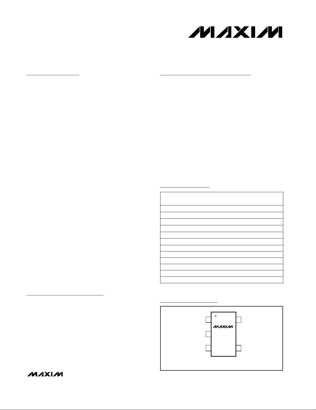
Pin Configurations
Pin Configurations continued at end of data sheet.
PIN-
PACKAGE
5 SOT23-5
5 SOT23-5
6 SOT23-6
6 SOT23-6
8 SO
8 SO
8 µMAX
8 µMAX
8 SO
8 SO
10 µMAX
10 µMAX-40°C to +85°C
-40°C to +85°C
-40°C to +85°C
-40°C to +85°C
-40°C to +85°C
-40°C to +85°C
-40°C to +85°C
-40°C to +85°C
-40°C to +85°C
-40°C to +85°C
-40°C to +85°C
-40°C to +85°C
TEMP. RANGEPART
MAX9040AEUK-T
MAX9040BEUK-T
MAX9041AEUT-T*
MAX9041BEUT-T*
MAX9041AESA*
MAX9041BESA*
MAX9042AEUA
MAX9042BEUA
MAX9042AESA
MAX9042BESA
MAX9043AEUB
MAX9043BEUB
TOP
MARK
ADNV
ADNX
AAHF
AAHH
—
—
—
—
—
—
—
—
TOP VIEW
15V
OUT
V
MAX9040
2
EE
MAX9050
CC
34
SOT23-5
REFIN+

dB
MAX9040–MAX9043/MAX9050–MAX9053
Micropower, Single-Supply,
SOT23 Comparator + Precision Reference ICs
2 _______________________________________________________________________________________
ABSOLUTE MAXIMUM RATINGS
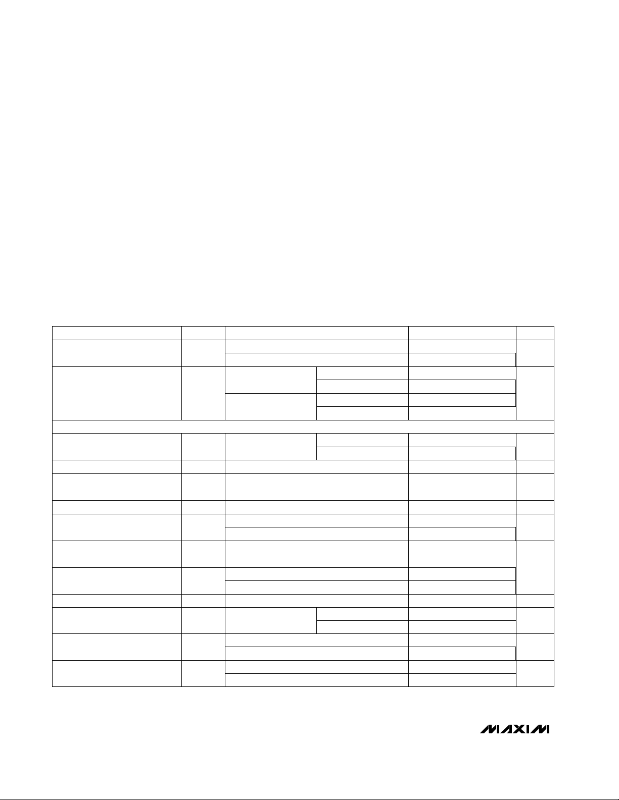
ELECTRICAL CHARACTERISTICS—A Grade (0.4% initial accuracy)
(VCC= +5V, VEE= 0, VCM= 0, I
OUT
= 0, I
REF
= 0, TA= T
MIN
to T
MAX
, unless otherwise noted. Typical values are at TA= +25°C.)
(Note 1)
Stresses beyond those listed under “Absolute Maximum Ratings” may cause permanent damage to the device. These are stress ratings only, and functional
operation of the device at these or any other conditions beyond those indicated in the operational sections of the specifications is not implied. Exposure to
absolute maximum rating conditions for extended periods may affect device reliability.
Supply Voltage (VCCto VEE) ....................................-0.3V to +6V
All Other Pins ...................................(V
EE
- 0.3V) to (VCC+ 0.3V)
Output Short-Circuit Duration
(OUT_, REF) .............Indefinite Short Circuit to Either Supply
Continuous Power Dissipation (T
A
= +70°C)
5-Pin SOT23 (derate 7.10mW/°C above +70°C)........571mW
6-Pin SOT23 (derate 8.70mW/°C above +70°C)........696mW
8-Pin µMAX (derate 4.1mW/°C above +70°C) ...........330mW
10-Pin µMAX (derate 5.6mW/°C above +70°C) .........444mW
8-Pin SO (derate 5.88mW/°C above +70°C)..............471mW
Operating Temperature Range ...........................-40°C to +85°C
Junction Temperature......................................................+150°C
Storage Temperature Range .............................-65°C to +150°C
Lead Temperature (soldering, 10s) .................................+300°C
VCC= 2.7V 35
VCC= 5V
2.3 2.55VCC= 2.7V, I
SOURCE
= 3.5mA
TA = -40°C to +85°C
TA= +25°C
VCC= 5.0V
VCC= 2.7V
VCC= 5.0V
VCC= 2.7V
PARAMETER SYMBOL MIN TYP MAX UNITS
60 85
55 80
Supply Current I
CC
45 60
µA
Input Offset Voltage (Note 3) V
OS
±0.5 ±5.0
mV
±7.0
Input Hysteresis V
HYST
±3.0 mV
Input Bias Current
(Notes 4, 5, 6)
I
B
±0.001 ±10.0 nA
Supply Voltage Range (Note 2) V
CC
2.5 5.5
V
2.7 5.5
40 55
Input Offset Current (Note 4) I
OS
±0.5 pA
Common-Mode Voltage Range
(Notes 4, 7)
CMVR
VEE- 0.25 V
CC
+ 0.25
V
V
EE
V
CC
Common-Mode Rejection Ratio
(Note 4)
CMRR 52 80
Power-Supply Rejection Ratio PSRR
55 80
55 80
Input Capacitance (Note 4) C
IN
2.5 pF
Output Short-Circuit Current I
SC
95
mA
Output Voltage Low V
OL
0.2 0.55
V
0.15 0.4
Output Voltage High V
OH
4.45 4.85
V
CONDITIONS
Specified common-mode range
TA= +25°C
Over entire commonmode range
TA= -40°C to +85°C
Specified common-mode range
Specified common-mode range
MAX9040–MAX9043, 2.5V ≤ VCC≤ 5.5V
MAX9050–MAX9053, 2.7V ≤ VCC≤ 5.5V
MAX9040–MAX9043
MAX9050–MAX9053
V
OUT
= VEEor V
CC
MAX9040/MAX9041/
MAX9050/MAX9051
VCC= 5V, I
SINK
= 8mA
VCC= 2.7V, I
SINK
= 3.5mA
VCC= 5V, I
SOURCE
= 8mA
dB
MAX9042/MAX9043/
MAX9052/MAX9053
COMPARATORS

MAX9040–MAX9043/MAX9050–MAX9053
Micropower, Single-Supply,
SOT23 Comparator + Precision Reference ICs
_______________________________________________________________________________________ 3
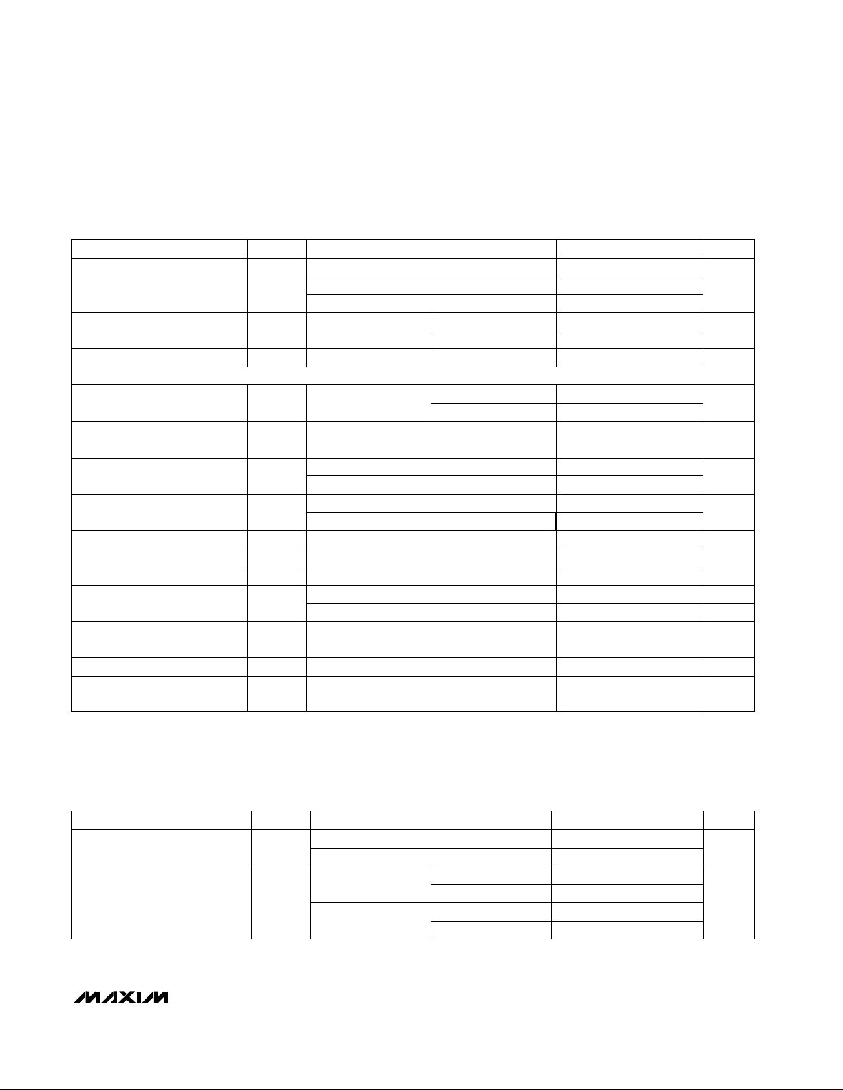
ELECTRICAL CHARACTERISTICS—A Grade (0.4% initial accuracy) (continued)
(VCC= +5V, VEE= 0, VCM= 0, I
OUT
= 0, I
REF
= 0, TA= T
MIN
to T
MAX
, unless otherwise noted. Typical values are at TA= +25°C.)
(Note 1)
ELECTRICAL CHARACTERISTICS—B Grade (1% initial accuracy)
(VCC= +5V, VEE= 0, VCM= 0, I
OUT
= 0, I
REF
= 0, TA= T
MIN
to T
MAX
, unless otherwise noted. Typical values are at TA= +25°C.)
(Note 1)
2.7V ≤ VCC≤ 5.5V, MAX9050–MAX9053
CONDITIONS UNITSMIN TYP MAXSYMBOLPARAMETER
CL= 15pF,
V
CC
= 2.7V
CL = 200pF
CL = 50pF
CL = 15pF
ns
450
tPD+/tPD-
Output Propagation Delay
(Note 8)
80
ns
50
Output Rise/Fall Times
40
tR/t
F
TA= +25°C
Time to V
OUT
valid logic state
V
2.040 2.048 2.056
V
REF
Output Voltage
µs20t
PU
Power-Up Time
2.5V ≤ VCC≤ 5.5V, MAX9040–MAX9043
µV/µA
∆V
REF
/
∆I
REF
Load Regulation
+50 +200
µV/V
+50 +200
∆V
REF
/
∆V
CC
Line Regulation
ppm/°C630TCV
REF
Output Voltage Temperature
Coefficient (Note 9)
2.490 2.500 2.510
50mV overdrive
MAX9040–MAX9043
MAX9050–MAX9053
1000h at TA= +25°C
V
REF
= VEEor V
CC
Sourcing: 0 ≤ I
REF
≤ 500µA
50Long-Term Stability
ppm130T
HYST
Thermal Hysteresis (Note 10)
mA4I
SC
Output Short-Circuit Current
24
400100mV overdrive
f = 0.1Hz to 10Hz µVp-p40
E
OUT
Noise Voltage
To V
REF
= 1% of final value
VCC= 5V ±100mV, f = 120Hz
f = 10Hz to 10kHz
nF0 4.7CL(V
REF
)
Capacitive Load Stability Range
(Note 6)
µs200tR(V
REF
)Turn-On Settling Time
dB84
∆V
REF
/
∆V
CC
Ripple Rejection
µV
RMS
105
ppm
3.5 6Sinking: -500µA ≤ I
REF
≤ 0
VOLTAGE REFERENCE
V
CC
I
CC
SYMBOL
VCC= 5.0V
VCC= 2.7V
VCC= 5.0V
VCC= 2.7V
MAX9040/MAX9041/
MAX9050/MAX9051
MAX9050–MAX9053
MAX9040–MAX9043
MAX9042/MAX9043/
MAX9052/MAX9053
CONDITIONS
40
2.7 5.5
V
2.5 5.5
Supply Voltage Range (Note 2)
45 100
µA
55
Supply Current
60 130
UNITSMIN TYP MAXPARAMETER

ns
MAX9040–MAX9043/MAX9050–MAX9053
Micropower, Single-Supply,
SOT23 Comparator + Precision Reference ICs
4 _______________________________________________________________________________________
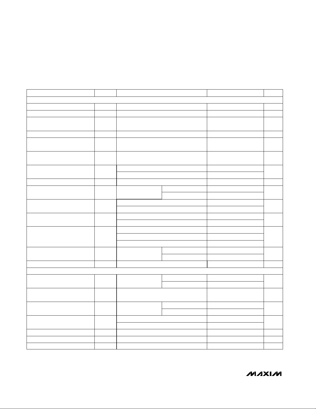
ELECTRICAL CHARACTERISTICS—B Grade (1% initial accuracy) (continued)
(VCC= +5V, VEE= 0, VCM= 0, I
OUT
= 0, I
REF
= 0, TA= T
MIN
to T
MAX
, unless otherwise noted. Typical values are at TA= +25°C.)
(Note 1)
∆V
REF
/
∆l
REF
I
SC
T
HYST
tR/t
F
∆V
REF
/
∆V
CC
TCV
REF
V
REF
t
PD+/tPD-
t
PU
PSRR
CMVR
CMRR
V
OH
V
OL
C
IN
I
SC
I
OS
I
B
V
HYST
V
OS
SYMBOL
MAX9050–MAX9053
MAX9040–MAX9043
MAX9040–MAX9043
MAX9050–MAX9053
50mV overdrive
VCC= 2.7V
VCC= 5V
Sinking: -500µA ≤ I
REF
≤ 0
Sourcing: 0 ≤ I
REF
≤ 500µA
V
REF
= VEEor V
CC
1000h at TA= +25°C
3.5 6
µV/mA
24
+50 +200
Load Regulation
mA
4
Output Short-Circuit Current
ppm
130
Thermal Hysteresis (Note 10)
ppm
100
Long-Term Stability
CL= 200pF
CL= 50pF
CL= 15pF
2.5V ≤ VCC≤ 5.5V
TA= +25°C
CL= 15pF,
VCC= 2.7V
Time to V
OUT
valid logic state
80
ns
50
40
Output Rise/Fall Times
µV/V
+50 +200
Line Regulation
ppm/°C
20 100
Output Voltage Temperature
Coefficient (Note 9)
2.475 2.500 2.525
V
2.028 2.048 2.068
Output Voltage
450
Output Propagation Delay
(Note 8)
400
µs
µs
20
Power-Up Time
MAX9040–MAX9043, 2.5V ≤ VCC≤ 5.5V
Specified common-mode range
VCC= 2.7V, I
SOURCE
= 3.5mA
VCC= 5V, I
SOURCE
= 8mA
VCC= 2.7V, I
SINK
= 3.5mA
VCC= 5V, I
SINK
= 8mA
MAX9050–MAX9053, 2.7V ≤ VCC≤ 5.5V
dB
55 80
Power-Supply Rejection Ratio
dB
52 80
V
V
EE
V
CC
Common-Mode Voltage Range
(Notes 4, 7)
Common-Mode Rejection Ratio
(Note 4)
2.55
V
4.45 4.85
Output Voltage High
0.15
V
0.2 0.55
Output Voltage Low
55 80
pF
2.5
Input Capacitance (Note 4)
mA
95
Output Short-Circuit Current
35
Specified common-mode range
Specified common-mode range
Over entire common-mode range
CONDITIONS
pA
±0.5
Input Offset Current (Note 4)
nA
±0.001 ±25.0
Input Bias Current
(Notes 4, 5, 6)
mV
±3.0
Input Hysteresis
mV
±1 ±9.0
Input Offset Voltage (Note 3)
UNITSMIN TYP MAXPARAMETER
V
OUT
= VEEor V
CC
ns
100mV overdrive
COMPARATOR
VOLTAGE REFERENCE
 Loading...