

Page 1
19-3241; Rev 1; 6/11
For pricing, delivery, and ordering information, please contact Maxim/Dallas Direct! at
1-888-629-4642, or visit Maxim’s website at www.maxim-ic.com.
UCSP, 1.8V, Nanopower, Beyond-the-Rails
Comparators With/Without Reference
General Description
The MAX9025–MAX9028 nanopower comparators in
space-saving chip-scale (UCSP™) packages feature
Beyond-the-Rails™ inputs and are guaranteed to operate down to +1.8V. The MAX9025/MAX9026 feature an
on-board 1.236V ±1% reference and draw an ultra-low
supply current of only 1µA, while the MAX9027/
MAX9028 (without reference) require just 0.6µA of supply
current. These features make the MAX9025–MAX9028
family of comparators ideal for all 2-cell batterymonitoring/management applications.
The unique design of the output stage limits supplycurrent surges while switching, virtually eliminating the
supply glitches typical of many other comparators. This
design also minimizes overall power consumption under
dynamic conditions. The MAX9025/MAX9027 have a
push-pull output stage that sinks and sources current.
Large internal-output drivers allow rail-to-rail output
swing with loads up to 5mA. The MAX9026/MAX9028
have an open-drain output stage that makes them suitable for mixed-voltage system design. All devices are
available in the miniature 6-bump UCSP packages.
Refer to the MAX9117 data sheet for similar comparators
in 5-pin SC70 packages and the MAX9017 data sheet for
similar dual comparators in 8-pin SOT23 packages.
Applications
2-Cell Battery Monitoring/Management
Ultra-Low-Power Systems
Mobile Communications
Notebooks and PDAs
Sensing at Ground or Supply Line
Telemetry and Remote Systems
Medical Instruments
Selector Guide
PART
MAX9025 Yes Push-Pull 1.0
MAX9026 Yes Open-Drain 1.0
MAX9027 No Push-Pull 0.6
MAX9028 No Open-Drain 0.6
Typical Application Circuit appears at end of data sheet.
INTERNAL
REFERENCE
OUTPUT
TYPE
SUPPLY
CURRENT
)
(µA
Features
♦ Space-Saving UCSP Package (1mm x 1.52mm)
♦ Ultra-Low Supply Current
0.6µA (MAX9027/MAX9028)
1µA with Reference (MAX9025/MAX9026)
♦ Guaranteed to Operate Down to +1.8V
♦ Internal 1.236V ±1% Reference (MAX9025/MAX9026)
♦ Input Voltage Range Extends 200mV
Beyond-the-Rails
♦ CMOS Push-Pull Output with ±5mA Drive
Capability (MAX9025/MAX9027)
♦ Open-Drain Output Versions Available
(MAX9026/MAX9028)
♦ Crowbar-Current-Free Switching
♦ Internal Hysteresis for Clean Switching
♦ No Phase Reversal for Overdriven Inputs
Ordering Information
PART
MAX9025EBT+T -
MAX9026EBT+T -40°C to +85°C 6 UCSP ADC
MAX9027EBT+T -40°C to +85°C 6 UCSP ADD
MAX9028EBT+T -40°C to +85°C 6 UCSP ADE
+Denotes a lead(Pb)-free/RoHS-compliant package.
T = Tape and reel.
TEMP
RANGE
40°C to +85°C 6 UCSP ADB
BUMPPACKAGE
TOP
MARK
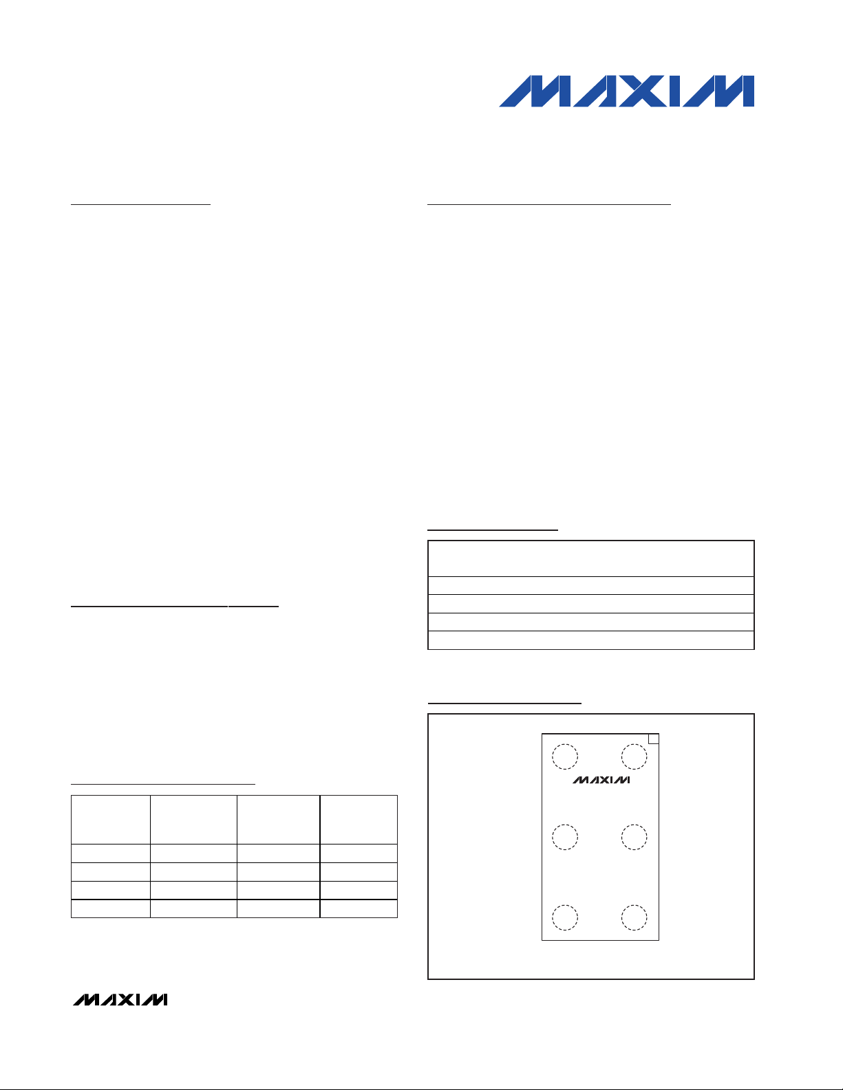
Pin Configurations
TOP VIEW
(BUMPS ON BOTTOM)
B
1
IN+
MAX9025–
MAX9028
REF
2
)
(V
EE
IN-
3
V
OUT
V
A
CC
EE
MAX9025–MAX9028
Beyond-the-Rails and UCSP are trademarks of Maxim Integrated
Products, Inc.
________________________________________________________________ Maxim Integrated Products 1
( ) MAX9027/MAX9028 PINS
UCSP
Page 2
MAX9025–MAX9028
UCSP, 1.8V, Nanopower, Beyond-the-Rails
Comparators With/Without Reference
2 _______________________________________________________________________________________
ABSOLUTE MAXIMUM RATINGS
ELECTRICAL CHARACTERISTICS—MAX9025/MAX9026 (WITH REF)
(VCC= +5V, VEE= 0V, V
IN+
= V
REF
, TA= -40°C to +85°C, unless otherwise noted. Typical values are at TA= +25°C.) (Note 1)
Stresses beyond those listed under “Absolute Maximum Ratings” may cause permanent damage to the device. These are stress ratings only, and functional
operation of the device at these or any other conditions beyond those indicated in the operational sections of the specifications is not implied. Exposure to
absolute maximum rating conditions for extended periods may affect device reliability.
Supply Voltage (VCCto VEE)..................................................+6V
Voltage Inputs (IN+, IN-, REF) .........(VEE- 0.3V) to (VCC+ 0.3V)
Output Voltage
MAX9025/MAX9027....................(VEE- 0.3V) to (VCC+ 0.3V)
MAX9026/MAX9028..................................(VEE- 0.3V) to +6V
Current into Input Pins ........................................................20mA
Output Current..................................................................±50mA
Output Short-Circuit Duration .................................................10s
Continuous Power Dissipation (TA= +70°C)
6-Bump UCSP (derate 3.9mW/°C above +70°C)........308mW
Operating Temperature Range ...........................-40°C to +85°C
Junction Temperature......................................................+150°C
Storage Temperature Range .............................-65°C to +150°C
Bump Temperature (soldering) Reflow............................+235°C
PARAMETER
CONDITIONS
Supply Voltage Range V
CC
Inferred from the PSRR test 1.8 5.5 V
VCC = 1.8V 0.8 1.5
TA = +25°C 1.0 1.7Supply Current I
CC
VCC = 5V
2.2
µA
IN+ Voltage Range V
IN+
Inferred from output swing test
V
EE
-
0.2
V
CC
+
0.2
V
TA = +25°C 0.3 5
Input Offset Voltage V
OS
(Note 2)
10
mV
Input-Referred Hysteresis V
HB
(Note 3) 4 mV
TA = +25°C
1
Input Bias Current I
B
TA = T
MIN
to T
MAX
2
nA
Power-Supply Rejection Ratio PSRR VCC = 1.8V to 5.5V 0.1 1
TA = +25°C
350
M AX 9025, V
C C
= 5V ,
I
S OU R C E
= 6m A
450
TA = +25°C 56 200
Output Voltage Swing High
V
CC
-
V
OH
M AX 9025, V
C C
=
300
mV
TA = +25°C
350
V
C C
= 5V ,
I
S I N K
= 6m A
450
TA = +25°C 57 200
Output Voltage Swing Low V
OL
V
C C
= 1.8V ,
I
S IN K
= 1m A
300
mV
Output Leakage Current I
LEAK
MAX9026 only, VO = 5.5V
1µA
VCC = 5V 35
Sourcing, VO = V
EE
VCC = 1.8V 3
VCC = 5V 33
Output Short-Circuit Current I
SC
Sinking, VO = V
CC
VCC = 1.8V 3
mA
VCC = 1.8V 7
High-to-Low Propagation Delay
(Note 4)
t
PD-
V
CC
= 5V 6
µs
SYMBOL
MIN TYP MAX UNITS
TA = T
MIN
to T
MAX
TA = T
MIN
to T
MAX
= T
MIN
MIN
MIN
MIN
to T
to T
to T
to T
MAX
MAX
MAX
MAX
TA = T
= 1m A
S OU RC E
T
A
TA = T
TA = T
1.8V , I
0.15
250
250
0.001
mV/V
Page 3
MAX9025–MAX9028
UCSP, 1.8V, Nanopower, Beyond-the-Rails
Comparators With/Without Reference
_______________________________________________________________________________________ 3
ELECTRICAL CHARACTERISTICS—MAX9027/MAX9028 (WITHOUT REF)
(VCC= +5V, VEE= 0V, VCM= 0V, TA= -40°C to +85°C, unless otherwise noted. Typical values are at TA= +25°C.) (Note 1)
ELECTRICAL CHARACTERISTICS—MAX9025/MAX9026 (WITH REF) (continued)
(VCC= +5V, VEE= 0V, V
IN+
= V
REF
, TA= -40°C to +85°C, unless otherwise noted. Typical values are at TA= +25°C.) (Note 1)
PARAMETER
SYMBOL
CONDITIONS
MIN
TYP
MAX
UNITS
VCC = 1.8V 11
MAX9025 only
V
CC
= 5V 28
VCC = 1.8V 12
Low-to-High Propagation Delay
(Note 4)
t
PD+
MAX9026 only,
R
PULLUP
= 100kΩ
V
CC
= 5V 31
µs
Rise Time t
RISE
MAX9025 only, CL = 15pF 1.6 µs
Fall Time t
FALL
CL = 15pF 0.2 µs
Power-Up Time t
ON
1.2 ms
TA = +25°C
Reference Voltage V
REF
TA = T
MIN
to T
MAX
V
Reference Voltage Temperature
Coefficient
TC
REF
40
°C
BW = 10Hz to 100kHz 29
Reference Output Voltage Noise
E
N
C
REF
= 1nF
BW = 10Hz to 6kHz 60
Reference Line Regulation
∆V
REF
/
∆V
CC
VCC = 1.8V to 5.5V 0.5
Reference Load Regulation
∆V
REF
/
∆I
OUT
∆I
OUT
= 0nA to 100nA
mV/
nA
1.224 1.236 1.248
1.205 1.267
0.03
ppm/
µV
mV/V
RMS
PARAMETER SYMBOL CONDITIONS MIN TYP MAX UNITS
Supply Voltage Range V
Input Common-Mode
Voltage Range
Input Offset Voltage V
Input-Referred Hysteresis V
Input Bias Current I
Power-Supply Rejection Ratio PSRR VCC = 1.8V to 5.5V 0.1 1 mV/V
Common-Mode Rejection Ratio CMRR (VEE - 0.2V) ≤ VCM ≤ (VCC + 0.2V) 0.5 3 mV/V
CC
CC
V
CM
OS
HB
B
Inferred from the PSRR test 1.8 5.5 V
VCC = 1.8V 0.45 0.75
VCC = 5V
Inferred from the CMRR test
-0.2V ≤ VCM ≤
+ 0.2V)
(V
(Note 2)
-0.2V ≤ VCM ≤ (VCC + 0.2V) (Note 3) 4 mV
TA = +25°C 0.15 1
TA = T
CC
to T
MIN
MAX
TA = +25°C 0.6 1.0Supply Current I
= T
MIN
to T
MAX
V
EE
T
A
0.2
TA = +25°C 0.3 5
= T
MIN
to T
MAX
T
A
µA
1.25
-
VCC +
0.2
V
mV
10
2
nA
Page 4
MAX9025–MAX9028
UCSP, 1.8V, Nanopower, Beyond-the-Rails
Comparators With/Without Reference
4 _______________________________________________________________________________________
ELECTRICAL CHARACTERISTICS—MAX9027/MAX9028 (WITHOUT REF) (continued)
(VCC= +5V, VEE= 0V, VCM= 0V, TA= -40°C to +85°C, unless otherwise noted. Typical values are at TA= +25°C.) (Note 1)
Note 1: All specifications are 100% tested at T
A
= +25°C. Specification limits over temperature (TA= T
MIN
to T
MAX
) are guaranteed
by design, not production tested.
Note 2: V
OS
is defined as the center of the hysteresis band at the input.
Note 3: The hysteresis-related trip points are defined as the edges of the hysteresis band, measured with respect to the center of
the band (i.e., V
OS
) (Figure 2).
Note 4: Specified with an input overdrive (V
OVERDRIVE
) of 100mV, and load capacitance of CL= 15pF. V
OVERDRIVE
is defined
above and beyond the offset voltage and hysteresis of the comparator input. For the MAX9025/MAX9026, reference voltage
error should also be added.
PARAMETER
CONDITIONS
UNITS
TA = +25°C
MAX9027 only, VCC =
5V, I
SOURCE
= 5mA
TA = +25°C58
Output Voltage Swing High
MAX9028 only, VCC =
mV
TA = +25°C
VCC = 5V,
I
SINK
= 5mA
TA = +25°C56
Output Voltage Swing Low V
OL
VCC = 1.8V,
I
SINK
= 1mA
mV
Output Leakage Current I
LEAK
MAX9028 only, VO = 5.5V
1µA
VCC = 5V 35
Sourcing, VO = V
EE
VCC = 1.8V 3
VCC = 5V 33
Output Short-Circuit Current I
SC
Sourcing, VO = V
CC
VCC = 1.8V 3
mA
VCC = 1.8V 16
High-to-Low Propagation Delay
(Note 4)
t
PD-
VCC = 5V 14
µs
VCC = 1.8V 15
MAX9027 only
V
CC
= 5V 40
VCC = 1.8V,
16
Low-to-High Propagation Delay
(Note 4)
t
PD+
MAX9028 only
V
CC
= 5V,
45
µs
Rise Time t
RISE
MAX9027 only, CL = 15pF 1.6 µs
Fall Time t
FALL
CL = 15pF 0.2 µs
Power-Up Time t
ON
1.2 ms
SYMBOL
VCC - V
OH
1.8V, I
SOURCE
= 1mA
TA = T
= T
T
A
TA = T
TA = T
MIN
MIN
MIN
MIN
to T
to T
to T
to T
MIN TYP MAX
191 400
MAX
MAX
191 400
MAX
MAX
0.001
500
200
300
500
200
300
R
R
PULLUP
PULLUP
= 100kΩ
= 100kΩ
Page 5
MAX9025/MAX9026
SUPPLY CURRENT vs. SUPPLY VOLTAGE
MAX9025-28 toc01
SUPPLY VOLTAGE (V)
SUPPLY CURRENT (nA)
4.53.52.5
800
1000
1200
600
1.5 5.5
TA = +85°C
TA = +25°C
TA = -40°C
MAX9025-28 toc02
SUPPLY VOLTAGE (V)
SUPPLY CURRENT (nA)
4.53.52.5
400
500
600
700
800
300
1.5 5.5
MAX9027/MAX9028
SUPPLY CURRENT vs. SUPPLY VOLTAGE
TA = +85°C
TA = +25°C
T
A
= -40°C
MAX9025-28 toc03
TEMPERATURE (°C)
SUPPLY CURRENT (nA)
603510-15
800
1000
1200
600
-40 85
MAX9025/MAX9026
SUPPLY CURRENT vs. TEMPERATURE
VCC = 5V
VCC = 1.8V
VCC = 3V
MAX9025-28 toc04
TEMPERATURE (°C)
SUPPLY CURRENT (nA)
603510-15
400
500
600
700
800
300
-40 85
VCC = 5V
VCC = 3V
MAX9027/MAX9028
SUPPLY CURRENT vs. TEMPERATURE
VCC = 1.8V
OUTPUT VOLTAGE LOW
vs. SINK CURRENT
MAX9025-28 toc07
SINK CURRENT (mA)
OUTPUT VOLTAGE LOW (mV)
8642
200
400
600
800
0
010
VCC = 5V
VCC = 3V
VCC = 1.8V
MAX9025-28 toc05
TRANSITION FREQUENCY (kHz)
SUPPLY CURRENT (µA)
101
5
10
15
20
25
30
35
40
0
0.1 100
MAX9025/MAX9026
SUPPLY CURRENT vs. OUTPUT
TRANSITION FREQUENCY
VCC = 5V
VCC = 3V
VCC = 1.8V
MAX9025-28 toc06
TRANSITION FREQUENCY (kHz)
SUPPLY CURRENT (µA)
101
5
10
15
20
25
30
35
40
0
0.1 100
MAX9027/MAX9028
SUPPLY CURRENT vs. OUTPUT
TRANSITION FREQUENCY
VCC = 5V
VCC = 3V
VCC = 1.8V
OUTPUT VOLTAGE LOW
vs. SINK CURRENT
MAX9025-28 toc08
SINK CURRENT (mA)
OUTPUT VOLTAGE LOW (mV)
8642
200
400
600
800
0
010
TA = +85°C
TA = +25°C
TA = -40°C
MAX9025/MAX9027
OUTPUT VOLTAGE HIGH vs. SOURCE CURRENT
MAX9025-28 toc09
SOURCE CURRENT (mA)
OUTPUT VOLTAGE HIGH (V
CC
- V
OH
, mV)
8642
200
400
600
800
0
010
VCC = 5V
VCC = 3V
VCC = 1.8V
MAX9025–MAX9028
UCSP, 1.8V, Nanopower, Beyond-the-Rails
Comparators With/Without Reference
_______________________________________________________________________________________ 5
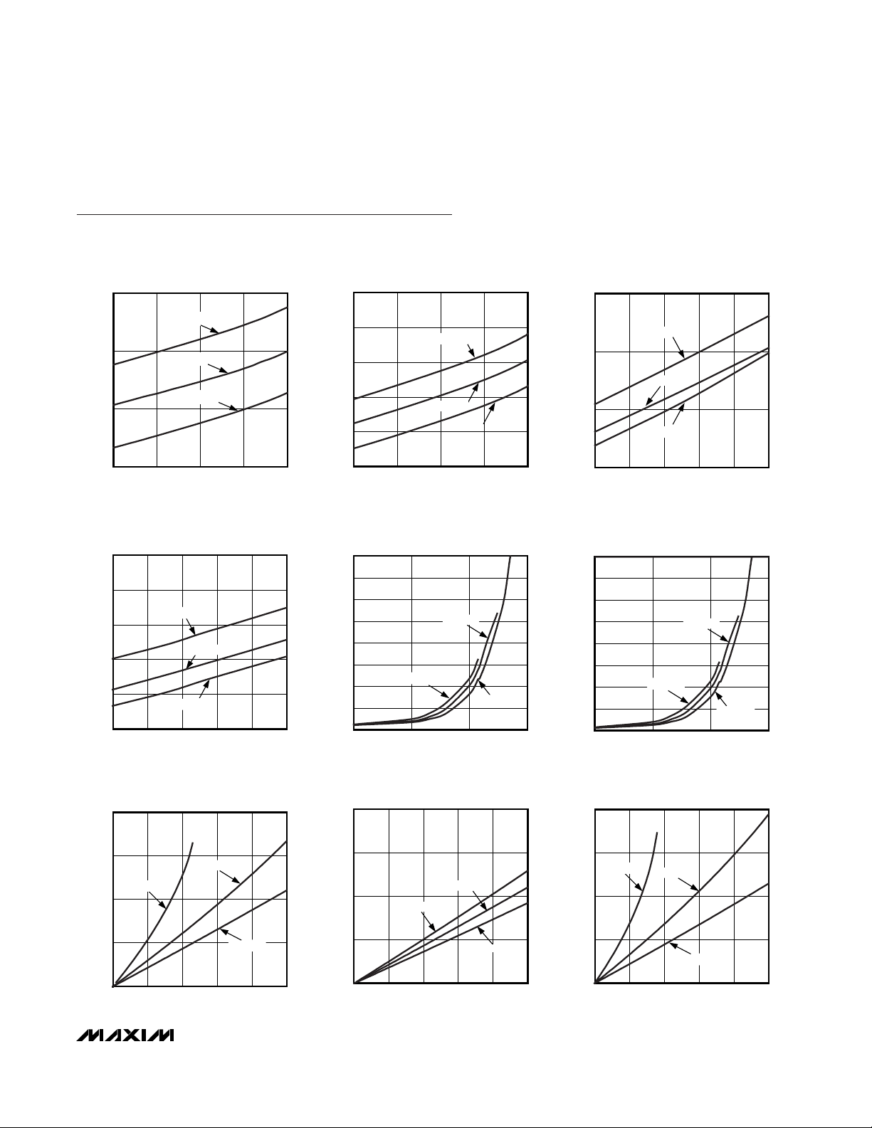
Typical Operating Characteristics
(VCC= +5V, V
EE
= 0V, CL= 15pF, V
OVERDRIVE
= 100mV, TA= +25°C, unless otherwise noted.)
Page 6

Typical Operating Characteristics (continued)
(VCC= +5V, V
EE
= 0V, CL= 15pF, V
OVERDRIVE
= 100mV, TA= +25°C, unless otherwise noted.)
MAX9025–MAX9028
UCSP, 1.8V, Nanopower, Beyond-the-Rails
Comparators With/Without Reference
6 _______________________________________________________________________________________
MAX9025/MAX9027
OUTPUT VOLTAGE HIGH vs. SOURCE CURRENT
MAX9025-28 toc10
SOURCE CURRENT (mA)
OUTPUT VOLTAGE HIGH (V
CC
- V
OH
, mV)
8642
200
400
600
800
0
010
TA = +85°C
TA = +25°C
TA = -40°C
SHORT-CIRCUIT SINK
CURRENT vs. TEMPERATURE
MAX9025-28 toc11
TEMPERATURE (°C)
SHORT-CIRCUIT SINK CURRENT (mA)
603510-15
10
20
30
40
0
-40 85
VCC = 5V
VCC = 3V
VCC = 1.8V
V
OUT
= V
CC
MAX9025/MAX9027 SHORT-CIRCUIT SOURCE
CURRENT vs. TEMPERATURE
MAX9025-28 toc12
TEMPERATURE (°C)
SHORT-CIRCUIT SINK CURRENT (mA)
603510-15
10
20
30
40
0
-40 85
VCC = 5V
VCC = 3V
VCC = 1.8V
V
OUT
= V
EE
OFFSET VOLTAGE
vs. TEMPERATURE
MAX9025-28 toc13
TEMPERATURE (°C)
OFFSET VOLTAGE (mV)
603510-15
0.3
0.5
0.8
1.0
0
-40 85
VCC = 5V
VCC = 3V
VCC = 1.8V
HYSTERESIS VOLTAGE
vs. TEMPERATURE
MAX9025-28 toc14
TEMPERATURE (°C)
HYSTERESIS VOLTAGE (mV)
603510-15
2.5
3.0
3.5
4.0
2.0
-40 85
VCC = 5V
VCC = 3V
VCC = 1.8V
-1.000
-0.600
0.200
-0.200
0.600
1.000
-0.5 1.50.5 2.5 3.5 4.5 5.5
INPUT BIAS CURRENT
vs. INPUT BIAS VOLTAGE
MAX9025-28 toc15
INPUT BIAS VOLTAGE (IN-) (V)
INPUT BIAS CURRENT (IN-) (nA)
IN+ = 2.5V
MAX9025/MAX9026
REFERENCE VOLTAGE vs. TEMPERATURE
MAX9025-28 toc16
TEMPERATURE (°C)
REFERENCE VOLTAGE (V)
603510-15
1.2340
1.2350
1.2360
1.2370
1.2330
-40 85
VCC = 5V
VCC = 3V
VCC = 1.8V
MAX9025/MAX9026
REFERENCE VOLTAGE vs. TEMPERATURE
MAX9025-28 toc17
TEMPERATURE (°C)
REFERENCE VOLTAGE (V)
603510-15
1.233
1.235
1.237
1.239
1.231
-40 85
5 DEVICES
MAX9025/MAX9026
REFERENCE VOLTAGE
vs. SUPPLY VOLTAGE
MAX9025-28 toc18
SUPPLY VOLTAGE (V)
REFERENCE VOLTAGE (V)
4.53.52.5
1.235
1.236
1.237
1.238
1.234
1.5 5.5
Page 7

Typical Operating Characteristics (continued)
(VCC= +5V, V
EE
= 0V, CL= 15pF, V
OVERDRIVE
= 100mV, TA= +25°C, unless otherwise noted.)
MAX9025–MAX9028
UCSP, 1.8V, Nanopower, Beyond-the-Rails
Comparators With/Without Reference
_______________________________________________________________________________________ 7
40
30
20
10
0
0.01 10.1 10 100
MAX9025/MAX9027
PROPAGATION DELAY (t
PD+
)
vs. CAPACITIVE LOAD
MAX9025-28 toc23
CAPACITIVE LOAD (nF)
t
PD+
(µs)
VCC = 5V
VCC = 3V
VCC = 1.8V
0
10
20
30
40
50
60
70
80
01020304050
PROPAGATION DELAY (t
PD-
)
vs. INPUT OVERDRIVE
MAX9025-28 toc24
INPUT OVERDRIVE (mV)
t
PD-
(µs)
VCC = 5V
VCC = 3V
VCC = 1.8V
0
20
10
40
30
50
60
02010 30 40 50
MAX9025/MAX9027
PROPAGATION DELAY (t
PD+
)
vs. INPUT OVERDRIVE
MAX9025-28 toc25
INPUT OVERDRIVE (mV)
t
PD+
(µs)
VCC = 5V
VCC = 3V
VCC = 1.8V
MAX9026/MAX9028
PROPAGATION DELAY (t
PD+
)
vs. PULLUP RESISTANCE
MAX9025-28 toc26
PULLUP RESISTANCE (kΩ)
t
PD+
(µs)
1000100
25
50
75
100
125
150
175
200
0
10 10000
VCC = 5V
VCC = 3V
VCC = 1.8V
20µs/div
PROPAGATION DELAY (VCC = 5V)
+100mV
MAX9025 toc27
-100mV
OUT
2V/div
0V
IN+
MAX9025/MAX9026
REFERENCE VOLTAGE
vs. REFERENCE CURRENT
MAX9025-28 toc19
REFERENCE CURRENT (nA)
REFERENCE VOLTAGE (V)
500-50
1.234
1.236
1.238
1.240
1.232
-100 100
VCC = 5V
VCC = 3V
VCC = 1.8V
PROPAGATION DELAY (t
PD-
)
vs. TEMPERATURE
MAX9025-28 toc20
TEMPERATURE (°C)
t
PD-
(µs)
603510-15
5
10
15
20
0
-40 85
VCC = 5V
VCC = 3V
VCC = 1.8V
MAX9025/MAX9027
PROPAGATION DELAY (t
PD+
)
vs. TEMPERATURE
MAX9025-28 toc21
TEMPERATURE (°C)
t
PD+
(µs)
603510-15
10
20
30
40
50
0
-40 85
VCC = 5V
VCC = 3V
VCC = 1.8V
20
15
10
5
0
0.01 10.1 10 100
PROPAGATION DELAY (t
PD-
)
vs. CAPACITIVE LOAD
MAX9025-28 toc22
CAPACITIVE LOAD (nF)
t
PD-
(µs)
VCC = 5V
VCC = 3V
VCC = 1.8V
Page 8

Typical Operating Characteristics (continued)
(VCC= +5V, V
EE
= 0V, CL= 15pF, V
OVERDRIVE
= 100mV, TA= +25°C, unless otherwise noted.)
MAX9025–MAX9028
UCSP, 1.8V, Nanopower, Beyond-the-Rails
Comparators With/Without Reference
8 _______________________________________________________________________________________
20µs/div
PROPAGATION DELAY (VCC = 1.8V)
+100mV
MAX9025 toc29
-100mV
OUT
1V/div
0V
IN+
200µs/div
1kHz FREQUENCY RESPONSE
(V
CC
= 5V)
+100mV
MAX9025 toc30
-100mV
OUT
2V/div
0V
IN+
20µs/div
PROPAGATION DELAY (VCC = 3V)
+100mV
MAX9025 toc28
-100mV
OUT
1V/div
0V
IN+
1ms/div
REFERENCE RESPONSE TO SUPPLY
VOLTAGE TRANSIENT (C
REF
= 10nF)
REF
200mV/div
MAX9025 toc32
V
CC
1V/div
1.8V
5V
40µs/div
POWER-UP/POWER-DOWN RESPONSE
V
CC
MAX9025 toc33
0V
OUT
2V/div
0V
2V/div
20µs/div
10kHz FREQUENCY RESPONSE
(V
CC
= 1.8V)
+100mV
MAX9025 toc31
-100mV
OUT
1V/div
0V
IN+
Page 9

MAX9025–MAX9028
UCSP, 1.8V, Nanopower, Beyond-the-Rails
Comparators With/Without Reference
_______________________________________________________________________________________ 9
Functional Diagrams
MAX9025
MAX9026
IN+
OUT
V
CC
V
EE
IN-
REF
1.236V
MAX9027
MAX9028
IN+
OUT
V
CC
V
EE
IN-
REF
Detailed Description
The MAX9025/MAX9026 feature an on-board 1.236V
±1% reference, yet draw an ultra-low supply current of
1.0µA. The MAX9027/MAX9028 (without reference)
consume just 0.6µA of supply current. All four devices
are guaranteed to operate down to +1.8V. Their common-mode input voltage range extends 200mV
beyond-the-rails. Internal hysteresis ensures clean output switching, even with slow-moving input signals.
Large internal output drivers allow rail-to-rail output
swing with up to ±5mA loads.
The output stage employs a unique design that minimizes supply-current surges while switching, virtually
eliminating the supply glitches typical of many other
comparators. The MAX9025/MAX9027 have a push-pull
output stage that sinks as well as sources current. The
MAX9026/MAX9028 have an open-drain output stage
that can be pulled beyond VCCto a maximum of 5.5V
above VEE. These open-drain versions are ideal for
implementing wire-OR output logic functions.
Input Stage Circuitry
The input common-mode voltage range extends from
V
EE
- 0.2V to VCC+ 0.2V. These comparators operate
at any differential input voltage within these limits. Input
bias current is typically ±0.15nA if the input voltage is
between the supply rails. Comparator inputs are protected from overvoltage by internal ESD protection
diodes connected to the supply rails. As the input voltage exceeds the supply rails, these ESD protection
diodes become forward biased and begin to conduct.
Output Stage Circuitry
The MAX9025–MAX9028 contain a unique breakbefore-make output stage capable of rail-to-rail operation with up to ±5mA loads. Many comparators
consume orders of magnitude more current during
switching than during steady-state operation. However,
with this family of comparators, the supply-current
change during an output transition is extremely small.
In the Typical Operating Characteristics, the Supply
Current vs. Output Transition Frequency graphs show
the minimal supply-current increase as the output
switching frequency approaches 1kHz. This characteristic reduces the need for power-supply filter capacitors to reduce glitches created by comparator
switching currents. In battery-powered applications,
this characteristic results in a substantial increase in
battery life.
PIN
FUNCTION
A2 A2
Comparator Output
A3 A3, B2
Negative Supply Voltage
B1 B1
Comparator Noninverting
Input
B2 —
1.236V Reference Output
A1 A1
Positive Supply Voltage
B3 B3 IN-
Comparator Inverting
Input
Pin Description
MAX9025/
MAX9026
MAX9027/
MAX9028
NAME
OUT
V
EE
IN+
REF
V
CC
Page 10

MAX9025–MAX9028
UCSP, 1.8V, Nanopower, Beyond-the-Rails
Comparators With/Without Reference
10 ______________________________________________________________________________________
Reference (MAX9025/MAX9026)
The MAX9025–MAX9028s’ internal +1.236V reference
has a typical temperature coefficient of 40ppm/°C over
the full -40°C to +85°C temperature range. The reference
is a very-low-power bandgap cell, with a typical 35kΩ
output impedance. REF can source and sink up to
100nA to external circuitry. For applications needing
increased drive, buffer REF with a low input-bias current
op amp such as the MAX4162. Most applications require
no REF bypass capacitor. For noisy environments or fast
VCCtransients, connect a 1nF to 10nF ceramic capacitor
from REF to GND.
Applications Information
Low-Voltage, Low-Power Operation
The MAX9025–MAX9028 are ideally suited for use with
most battery-powered systems. Table 1 lists a variety of
battery types, capacities, and approximate operating
times for the MAX9025–MAX9028, assuming nominal
conditions.
Internal Hysteresis
Many comparators oscillate in the linear region of operation because of noise or undesired parasitic feedback.
This tends to occur when the voltage on one input is
equal or very close to the voltage on the other input. The
MAX9025–MAX9028 have internal 4mV hysteresis to
counter parasitic effects and noise.
The hysteresis in a comparator creates two trip points:
one for the rising input voltage (V
THR
) and one for the
falling input voltage (V
THF
) (Figure 2). The difference
between the trip points is the hysteresis (VHB). When
the comparator’s input voltages are equal, the hysteresis effectively causes one comparator input to move
quickly past the other, thus taking the input out of the
region where oscillation occurs. Figure 2 illustrates the
case in which IN- has a fixed voltage applied, and IN+
is varied. If the inputs were reversed, the figure would
be the same, except with an inverted output.
Adding External Hysteresis
In applications requiring more than the internal 4mV
hysteresis of the MAX9025–MAX9028, additional hysteresis can be added with external components.
Because the MAX9025–MAX9028 are intended for very
low-power systems, care should be taken to minimize
power dissipation in the additional circuitry.
Regardless of which approach is taken, the external
hysteresis will be V
CC
dependent. Over the full discharge
range of battery-powered systems, the hysteresis can
change as much as 40%. This must be considered
during design.
BANDGAP
REF
V
EE
V
CC
Figure 1. MAX9025/MAX9026 Voltage Reference Output
Equivalent Circuit
Table 1. Battery Applications Using MAX9025–MAX9028
BATTERY
TYPE
RECHARGEABLE
V
FRESH
(V)
V
END-OF-LIFE
(V)
CAPACITY,
AA SIZE
(mA-H)
MAX9025/MAX9026
OPERATING TIME
(hr)
MAX9027/MAX9028
OPERATING TIME
(hr)
Alkaline
(2 Cells)
No 3.0 1.8 2000 1.8 x 10
6
2.8 x 10
6
NickelCadmium
(2 Cells)
Yes 2.4 1.8 750 680,000 1.07 x 10
6
Lithium-Ion
(1 Cell)
Yes 3.5 2.7 1000 0.9 x 10
6
1.4 x 10
6
Nickel-MetalHydride
(2 Cells)
Yes 2.4 1.8 1000 0.9 x 10
6
1.4 x 10
6
Page 11

MAX9025–MAX9028
UCSP, 1.8V, Nanopower, Beyond-the-Rails
Comparators With/Without Reference
______________________________________________________________________________________ 11
THRESHOLDS
OUT
IN+
IN-
V
HB
HYSTERESIS
BAND
V
THF
V
THR
Figure 2. Threshold Hysteresis Band
V
CC
MAX9027
OUT
R
S
R
FB
VCC/2
VIN
Figure 3. MAX9025/MAX9027 External Hysteresis
Simplest Circuit
The simplest circuit for adding external hysteresis is
shown in Figure 3. In this example, the hysteresis is
defined by:
where RSis the source resistance and RFBis the feedback resistance. Because the comparison threshold is
1/2 VCC, the MAX9027 was chosen for its push-pull output and lack of reference. This provides symmetrical
hysteresis around the threshold.
Output Considerations
In most cases, the push-pull outputs of the
MAX9025/MAX9027 are best for external hysteresis.
The open-drain output of the MAX9026/MAX9028 can
be used, but the effect of the feedback network on the
actual output high voltage must be considered.
Component Selection
Because the MAX9025–MAX9028 are intended for very
low power-supply systems, the highest impedance circuits should be used wherever possible. The offset
error due to input-bias current is proportional to the
total impedance seen at the input. For example, selecting components for Figure 3, with a target of 50mV hysteresis, a 5V supply, and choosing an R
FB
of 10MΩ
gives RSas 100kΩ. The total impedance seen at IN+ is
therefore 10MΩ || 100kΩ, or 99kΩ. The maximum IBof
the MAX9025–MAX9028 is 2nA; therefore, the error due
to source impedance is less than 400µV.
Asymmetrical Hysteresis
When the input threshold is not set at 1/2 VCC, the hysteresis added to the input threshold will not be symmetrical. This is typical of the MAX9025/MAX9026 where
the internal reference is usually used as the threshold.
If the asymmetry is unacceptable, it can be corrected
by adding resistors to the circuit.
Board Layout and Bypassing
Power-supply bypass capacitors are not typically needed, but use 100nF bypass capacitors close to the
device’s supply pins when supply impedance is high,
supply leads are long, or excessive noise is expected
on the supply lines. Minimize signal trace lengths to
reduce stray capacitance. A ground plane and surfacemount components are recommended. If the REF pin is
decoupled, use a new low-leakage capacitor.
Zero-Crossing Detector
Figure 4 shows a zero-crossing detector application.
The MAX9027’s inverting input is connected to ground,
and its noninverting input is connected to a 100mV
P-P
signal source. As the signal at the noninverting input
crosses 0V, the comparator’s output changes state.
Logic-Level Translator
The Typical Application Circuit shows an application
that converts 5V logic to 3V logic levels. The MAX9028
is powered by the +5V supply voltage, and the pullup
resistor for the MAX9028’s open-drain output is connected to the +3V supply voltage. This configuration
allows the full 5V logic swing without creating overvoltage on the 3V logic inputs. For 3V to 5V logic-level
translations, simply connect the +3V supply voltage to
VCCand the +5V supply voltage to the pullup resistor.
Hysteresis
R
R
V
S
FB
CC
=×
Page 12

MAX9025–MAX9028
UCSP, 1.8V, Nanopower, Beyond-the-Rails
Comparators With/Without Reference
12 ______________________________________________________________________________________
UCSP Applications Information
For the latest application details on UCSP construction,
dimensions, tape carrier information, printed circuit board
techniques, bump-pad layout, and recommended reflow
temperature profiles, as well as the latest information on
reliability testing results, go to Maxim’s web site at
www.maxim-ic.com/ucsp to find the Application Note:
UCSP—A Wafer-Level Chip-Scale Package.
Chip Information
TRANSISTOR COUNT: 209
PROCESS: BiCMOS
MAX9028
IN-
2MΩ
2MΩ
R
PULLUP
3V (5V)
LOGIC OUT
OUT
V
CC
+5V (+3V)
+3V (+5V)
V
EE
5V (3V) LOGIC IN
IN+
LOGIC-LEVEL
TRANSLATOR
Typical Application Circuit
MAX9027
IN+
OUT
V
CC
100mV
P-P
V
CC
V
EE
IN-
Figure 4. Zero-Crossing Detector
Page 13

UCSP, 1.8V, Nanopower, Beyond-the-Rails
Comparators With/Without Reference
Package Information
For the latest package outline information and land patterns, go to www.maxim-ic.com/packages. Note that a “+”, “#”, or “-” in the
package code indicates RoHS status only. Package drawings may show a different suffix character, but the drawing pertains to the
package regardless of RoHS status.
PACKAGE TYPE PACKAGE CODE OUTLINE NO. LAND PATTERN NO.
6 UCSP B6+1
21-0097
Refer to Application Note 1891
6L, UCSP.EPS
MAX9025–MAX9028
PACKAGE OUTLINE, 3x2 UCSP
21-0097
______________________________________________________________________________________ 13
1
G
1
Page 14

UCSP, 1.8V, Nanopower, Beyond-the-Rails
Comparators With/Without Reference
Revision History
REVISION
NUMBER
0 5/04 Initial release. —
1 6/11 Added information for lead-free versions 1
REVISION
DATE
MAX9025–MAX9028
DESCRIPTION
PAGES
CHANGED
Maxim cannot assume responsibility for use of any circuitry other than circuitry entirely embodied in a Maxim product. No circuit patent licenses are
implied. Maxim reserves the right to change the circuitry and specifications without notice at any time.
14
____________________Maxim Integrated Products, 120 San Gabriel Drive, Sunnyvale, CA 94086 408-737-7600
© 2011 Maxim Integrated Products Maxim is a registered trademark of Maxim Integrated Products, Inc.
 Loading...