

For free samples & the latest literature: http://www.maxim-ic.com, or phone 1-800-998-8800.
For small orders, phone 408-737-7600 ext. 3468.
General Description
The MAX9000 family features the combination of a highspeed operational amplifier, a 185ns comparator, and a
precision 1.230V reference. These devices operate from a
single +2.5V to +5.5V supply and draw less than 500µA of
quiescent current. The MAX9001/MAX9004 feature a shutdown mode that reduces supply current to 2µA and puts
the outputs into a high-impedance state, making them
ideal for portable and battery-powered applications.
The amplifiers in the MAX9000/MAX9001/MAX9002 are
unity-gain stable with a 1.25MHz gain-bandwidth product,
while the amplifiers in the MAX9003/MAX9004/MAX9005
are stable for closed-loop gains of +10V/V or greater with
an 8MHz gain-bandwidth product. The input commonmode voltage extends from 150mV below the negative
supply to within 1.2V of the positive supply for the amplifier, and to within 1.1V for the comparator. The amplifier and
comparator outputs can swing Rail-to-Rail®and deliver up
to ±2.5mA and ±4.0mA, respectively, to an external load
while maintaining excellent DC accuracy. The unique
design of the comparator output stage substantially
reduces switching current during output transitions, virtually
eliminating power-supply glitches.
The comparator’s ±2mV of built-in hysteresis provides
noise immunity and prevents oscillations even with a
slow-moving input signal. The MAX9000/MAX9001/
MAX9003/MAX9004 have an internal 1.230V ±1% precision reference with a low 8ppm/°C temperature coefficient that can sink or source up to 1mA. The amplifier and
reference are stable with capacitive loads up to 250pF
and 100nF, respectively. The comparator’s inverting input
is internally connected to the reference output in the
MAX9000/MAX9003.
________________________Applications
Single-Supply Zero- Photodiode Preamps
Crossing Detector
Smart Card Readers
Instruments, Terminals, Infrared Receivers
and Bar-Code Readers for Remote Controls
Keyless Entry Sensor Signal Detection
Features
♦ Op Amp + Comparator + Reference in
Space-Saving µMAX Package
♦ +2.5V to +5.5V Single-Supply Voltage Range
♦ 340µA Supply Current (MAX9002/MAX9005)
♦ Unity-Gain Stable (GBW = 1.25MHz) and
Decompensated (AV≥ 10V/V, GBW = 8MHz) Options
♦ Op-Amp/Comparator Outputs Swing Rail-to-Rail
♦ Ground-Sensing Inputs for Both Op Amp and
Comparator
♦ Op Amp Stable with Capacitive Loads up to 250pF
♦ Internal ±2mV Comparator Hysteresis
♦ Fast 185ns Propagation-Delay Comparator
♦ No Phase Reversal for Overdriven Inputs
(Both Op Amp and Comparator)
♦ Internal 1.230V Precision Reference (MAX9000/
MAX9001/MAX9003/MAX9004)
±1% Initial Accuracy
Low 8ppm/°C Temperature Drift
Sink or Source up to 1mA
Stable for Capacitive Loads up to 100nF
MAX9000–MAX9005
Low-Power, High-Speed, Single-Supply
Op Amp + Comparator + Reference ICs
________________________________________________________________
Maxim Integrated Products
1
19-0499; Rev 1; 7/98
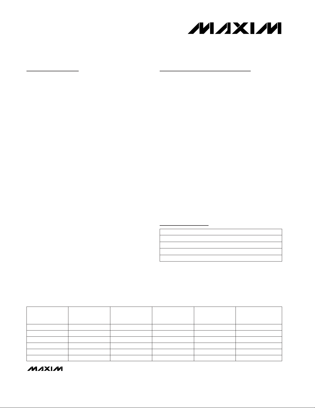
PART
MAX9000EUA
MAX9000ESA -40°C to +85°C
-40°C to +85°C
TEMP. RANGE PIN-PACKAGE
8 µMAX
8 SO
Ordering Information
Ordering Information continued at end of data sheet.
Rail-to-Rail is a registered trademark of Nippon Motorola, Ltd.
Pin Configurations and Typical Operating Circuit appear at
end of data sheet.
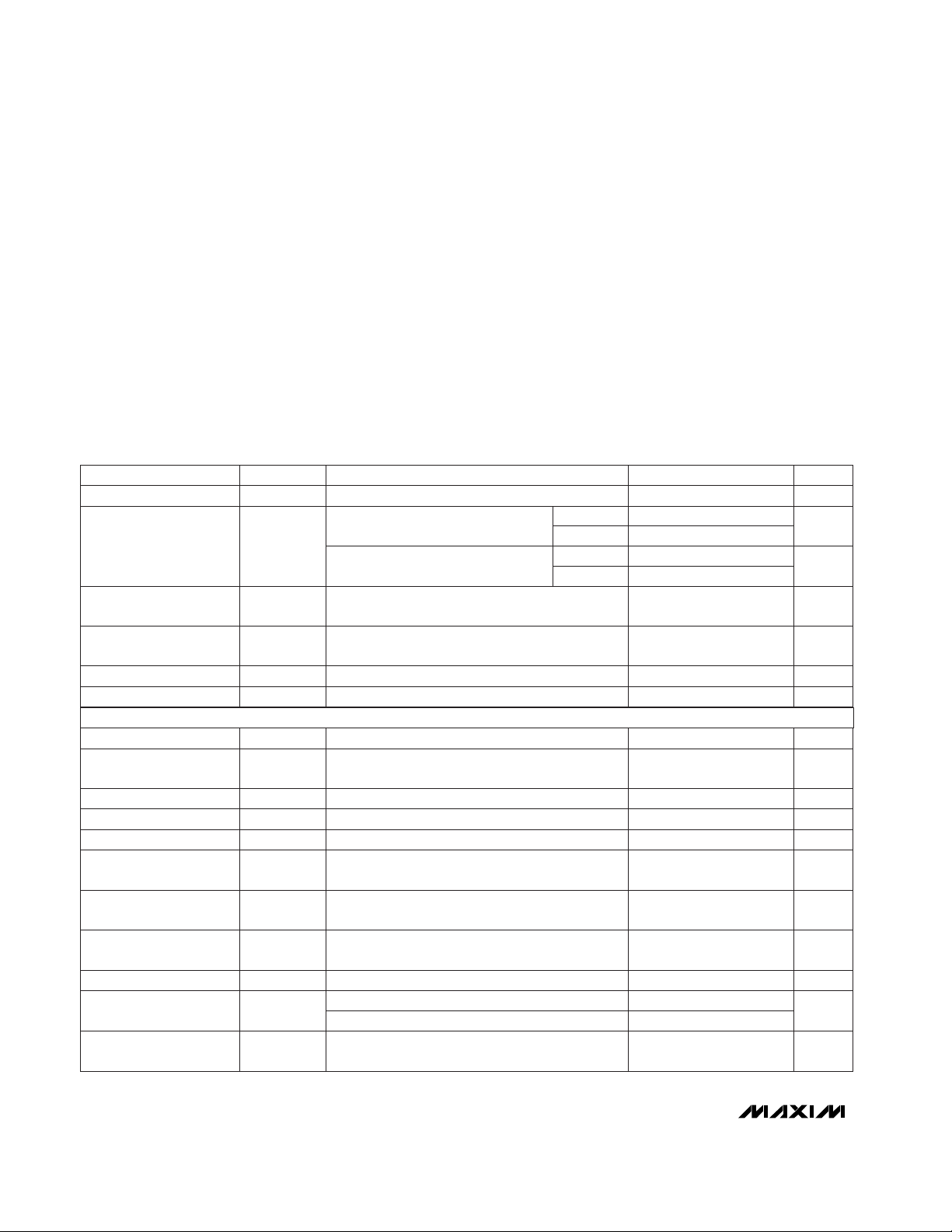
INTERNAL
PRECISION
REFERENCE
PIN-PACKAGE
MAX9000 Yes 8 SO/µMAX
MAX9001 Yes 10 µMAX, 14 SO
PART
MAX9002 No 8 SO/µMAX
OP-AMP GAIN
STABILITY
(V/V)
1
1
1
MAX9003 Yes 8 SO/µMAX
MAX9004 Yes 10 µMAX, 14 SO
MAX9005 No 8 SO/µMAX
10
10
10
SHUTDOWN
No
Yes
No
No
Yes
No
OP-AMP GAIN
BANDWIDTH
(MHz)
1.25
1.25
1.25
8
8
8
______________________________________________________________________________Selector Guide
MAX9001EUB
MAX9001ESD -40°C to +85°C
-40°C to +85°C 10 µMAX
14 SO
MAX9000–MAX9005
Low-Power, High-Speed, Single-Supply
Op Amp + Comparator + Reference ICs
2 _______________________________________________________________________________________
ABSOLUTE MAXIMUM RATINGS
ELECTRICAL CHARACTERISTICS
(VDD= +2.5V to +5.5V, VSS= 0, SHDN = VDD(MAX9001/MAX9004 only), V
CM(OP AMP)
= 0, V
AOUT
= VDD/ 2, V
CM(COMP)
= 0 (for
MAX9001/MAX9002/MAX9004/MAX9005), COUT = low, I
OUT(REF)
= 0, TA= T
MIN
to T
MAX
, unless otherwise noted. Typical values are
at V
DD
= 5V and TA= +25°C.)
Stresses beyond those listed under “Absolute Maximum Ratings” may cause permanent damage to the device. These are stress ratings only, and functional
operation of the device at these or any other conditions beyond those indicated in the operational sections of the specifications is not implied. Exposure to
absolute maximum rating conditions for extended periods may affect device reliability.
Supply Voltage (VDDto VSS)....................................-0.3V to +6V
Voltage Inputs (AIN_, CIN_).............(V
SS
- 0.3V) to (VDD+ 0.3V)
Output Short-Circuit Duration (AOUT, COUT, REF)...Continuous
to either V
SS
or V
DD
Continuous Power Dissipation (TA= +70°C)
8-Pin SO (derate 5.88mW/°C above +70°C).................471mW
8-Pin µMAX (derate 4.1mW/°C above +70°C)..............330mW
10-Pin µMAX (derate 5.6mW/°C above +70°C)............444mW
14-Pin SO (derate 8.3mW/°C above +70°C).................667mW
Operating Temperature Range
MAX900_E _ _...................................................-40°C to +85°C
Maximum Junction Temperature .....................................+150°C
Storage Temperature Range.............................-65°C to +160°C
Lead Temperature (soldering, 10sec).............................+300°C
V
SHDN
≤ (0.3V x VDD), V
AOUT
= 0 to V
DD
Shorted to V
DD
Shorted to V
SS
MAX9000/MAX9001/
MAX9003/MAX9004
AV= 1V/V
VDD= 2.5V to 5.5V
MAX900_ES_, (VSS- 0.15V) ≤ VCM≤ (VDD- 1.2V),
VDD= 5.5V
Guaranteed by PSRR tests
Guaranteed by CMRR test
Differential or common mode
MAX900_ES_
AIN+, AIN-
AIN+, AIN-
MAX9002/MAX9005
MAX9001/MAX9004 (V
SHDN
= 0)
MAX900_ES_
CONDITIONS
µA±0.01 ±1
I
OUT
(DISABLED)
Disabled Mode Output
Leakage
mA
65
Output Short-Circuit
Current
10
Ω0.01Output Resistance
dB74 100PSRR
Power-Supply Rejection
Ratio
dBCMRR
Common-Mode
Rejection Ratio
72 96
V-0.15 VDD- 1.2CMVR
Input Common-Mode
Voltage Range
MΩ1000R
IN
Input Resistance
nA±0.02 ±1Input Offset Current
nA±0.05 ±2I
BIAS
Input Bias Current
µV/°CTCV
OS
Input Offset Voltage
Temperature Coefficient
±1
µA
450 550
410 500
V2.5 5.5V
DD
Supply Voltage Range
V
OS
Input Offset Voltage mV±0.5 ±1.5
V0.3 x V
DD
V
IL(
SHDN
)
Shutdown Logic Low
340 425
µA
375 475
I
DD
Supply Current
µA2 5I
SHDN
Supply Current in
Shutdown
V0.7 x V
DD
V
IH(
SHDN
)
Shutdown Logic High
UNITSMIN TYP MAXSYMBOLPARAMETER
VDD= 3V
VDD= 5V
VDD= 3V
VDD= 5V
MAX9001/MAX9004 (V
SHDN
= 0 to VDD) µA1 2.5I
IN(
SHDN
)
Shutdown Input Bias
Current
OP AMP
MAX9000–MAX9005
Low-Power, High-Speed, Single-Supply
Op Amp + Comparator + Reference ICs
_______________________________________________________________________________________ 3
f = 10kHz
f = 10kHz
V
AIN+
- V
AIN-
≥ 10mV
VDD= 5.5V
VDD= 2.5V
CONDITIONS
fA/√Hz
1I
NOISE
Input Noise Current Density
nV/√Hz
36V
NOISE
Input Noise Voltage Density
pF2.5C
IN
Input Capacitance
140 250
1 5
1 5
94 125
dB
86 106
A
VOL
Large-Signal Voltage Gain
84 115
94 120
UNITSMIN TYP MAXSYMBOLPARAMETER
ELECTRICAL CHARACTERISTICS (continued)
(VDD= +2.5V to +5.5V, VSS= 0, SHDN = VDD(MAX9001/MAX9004 only), V
CM(OP AMP)
= 0, V
AOUT
= VDD/ 2, V
CM(COMP)
= 0 (for
MAX9001/MAX9002/MAX9004/MAX9005), COUT = low, I
OUT(REF)
= 0, TA= T
MIN
to T
MAX
, unless otherwise noted. Typical values are
at V
DD
= 5V and TA= +25°C.)
MAX9003/MAX9004/MAX9005
MAX9000/MAX9001/MAX9002
MHz
8
GBWGain-Bandwidth Product
1.25
mV
60 100
VOL/ V
OH
Output Voltage Swing
0.009
MAX9000/MAX9001/MAX9002
MAX9000/MAX9001/MAX9002
dB
30
degrees
75
µs2Power-On Time
µs2Enable Delay Time
µs0.2Shutdown Delay Time
MAX9000/MAX9001/MAX9002 (AV= 1V/V) 250
V
AOUT
= 0.05V to 2.45V, RL= 100kΩ
V
AOUT
= 0.2V to 2.3V, RL= 1kΩ
V
AOUT
= 0.05V to 5.4V, RL= 100kΩ
V
AOUT
= 0.25V to 5.2V, RL= 1kΩ
VDD- V
OH
V
OL
VDD- V
OH
V
OL
MAX9000/MAX9001/
MAX9002 (AV= 1V/V)
f = 10kHz,
V
AOUT
= 2Vp-p,
VDD= 5V
%
0.028
THD+N
Total Harmonic Distortion
plus Noise
MAX9003/MAX9004/
MAX9005 (AV= 10V/V)
VDD= 5V,
V
AOUT
= 4V step
µs
6.9
2.1
Settling Time to within 0.01%
MAX9000/MAX9001/
MAX9002 (AV= 1V/V)
MAX9003/MAX9004/
MAX9005 (AV= 10V/V)
MAX9003/MAX9004/MAX9005 (AV= 10V/V)
pF
250
C
LOAD
Capacitive-Load Stability
µV/°CTCV
OS
Input Offset Voltage
Temperature Coefficient
MAX900_ES_ ±1
mVInput-Referred Hysteresis VDD= 5V (Notes 2, 3) 4 7
RL = 100kΩ
RL = 1kΩ
MAX9003/MAX9004/MAX9005 80
Phase Margin
MAX9003/MAX9004/MAX9005 40
Gain Margin
mVV
OS
Input Offset Voltage MAX900_ES_ (Notes 1, 2) ±1 ±2
VDD= 5V,
V
AOUT
= 4V step
V/µs
0.85
6.0
SRSlew Rate
MAX9000/MAX9001/
MAX9002 (AV= 1V/V)
MAX9003/MAX9004/
MAX9005 (AV= 10V/V)
COMPARATOR
MAX9000–MAX9005
Low-Power, High-Speed, Single-Supply
Op Amp + Comparator + Reference ICs
4 _______________________________________________________________________________________
VDD= 5V, RL= 10kΩ, CL= 15pF (Note 5)
VOD= 25mV, RL= 10kΩ, CL= 15pF (Note 4)
V
SHDN
≤ (0.3V x VDD), V
COUT
= 0 to V
DD
MAX9001/MAX9002/MAX9004/MAX9005,
0.15V ≤ V
CM
≤ (VDD- 1.1V), VDD= 5.5V
(V
CIN+
- V
CIN-
)
≥ 20mV
VDD= 2.5V to 5.5V
CONDITIONS
ns100Power-On Time
ns100Enable Delay Time
ns100Shutdown Delay Time
ns10tR, t
F
Rise/Fall Time
ns185t
PD+
, t
PD-
Propagation Delay
µA±0.01 ±1
I
OUT
(DISABLED)
Disabled Mode Output
Leakage
mA55
Output Short-Circuit
Current
mV
400
VOL/V
OH
Output Voltage Swing
5
nA8 80I
BIAS
Input Bias Current
400
5
dB72 100CMRR
Common-Mode
Rejection Ratio
dB72 100PSRR
Power-Supply Rejection
Ratio
UNITSMIN TYP MAXSYMBOLPARAMETER
Note 1: Comparator Input Offset is defined as the center of the input-referred hysteresis zone.
Note 2: Measured at V
CM(COMP)
= 0 for the MAX9001/MAX9002/MAX9004/MAX9005; or V
CM(COMP)
= V
REF
for the MAX9000/MAX9003.
Note 3: Input-referred hysteresis is defined as the difference of the trip points required to change comparator output states.
Note 4: V
OD
is the overdrive that is beyond the offset and hysteresis-determined trip points.
Note 5: Rise and fall times are measured between 10% and 90% at COUT.
ELECTRICAL CHARACTERISTICS (continued)
(VDD= +2.5V to +5.5V, VSS= 0, SHDN = VDD(MAX9001/MAX9004 only), V
CM(OP AMP)
= 0, V
AOUT
= VDD/ 2, V
CM(COMP)
= 0 (for
MAX9001/MAX9002/MAX9004/MAX9005), COUT = low, I
OUT(REF)
= 0, TA= T
MIN
to T
MAX
, unless otherwise noted. Typical values are
at V
DD
= 5V and TA= +25°C.)
Shorted to V
DD
Shorted to V
SS
V
DD
= 5V,
I
OUT
= 0 to 1mA
V
DD
= 2.5V to 5.5V
MAX900_ES_, V
DD
= 5V, TA = +25°C
mA
10
6
Output Short-Circuit
Current
0.15 0.8
µV/V20 250Line Regulation
ppm/°C8TCV
REF
Output Voltage
Temperature Coefficient
VV
REF
Output Voltage 1.218 1.230 1.242
mV/mA
0.6 2.0
Load Regulation
0.1Hz to 10Hz
V
SHDN
≤ (0.3V x VDD), V
REF
= 0 to V
DD
µVp-p20Output Noise
µA±0.01 ±1
Disabled Mode Output
Leakage
RL= 100kΩ to VSS, V
REF
within 1% µs16Enable Delay Time
µs1Shutdown Delay Time
RL= 100kΩ to VSS, V
REF
within 1%
nF0 to 100Capacitive Load Stability
µs16Power-On Time
VDD- V
OH
I
SOURCE
= 10µA
I
SOURCE
= 4mA
I
SINK
= 10µA
I
SINK
= 4mA
V
OL
Sourcing
Sinking mV/mA
Guaranteed by CMRR test V
VSS- VDD-
0.15 1.1
V
CM
Common-Mode
Voltage Range
VOLTAGE REFERENCE (MAX9000/MAX9001/MAX9003/MAX9004)
Input Offset Current I
OS
MAX9001/MAX9002/MAX9004/MAX9005 ±2 ±15 nA
MAX9000–MAX9005
Low-Power, High-Speed, Single-Supply
Op Amp + Comparator + Reference ICs
_______________________________________________________________________________________
5
200
300
250
400
350
450
500
2.5 3.5 4.03.0 4.5 5.0 5.5
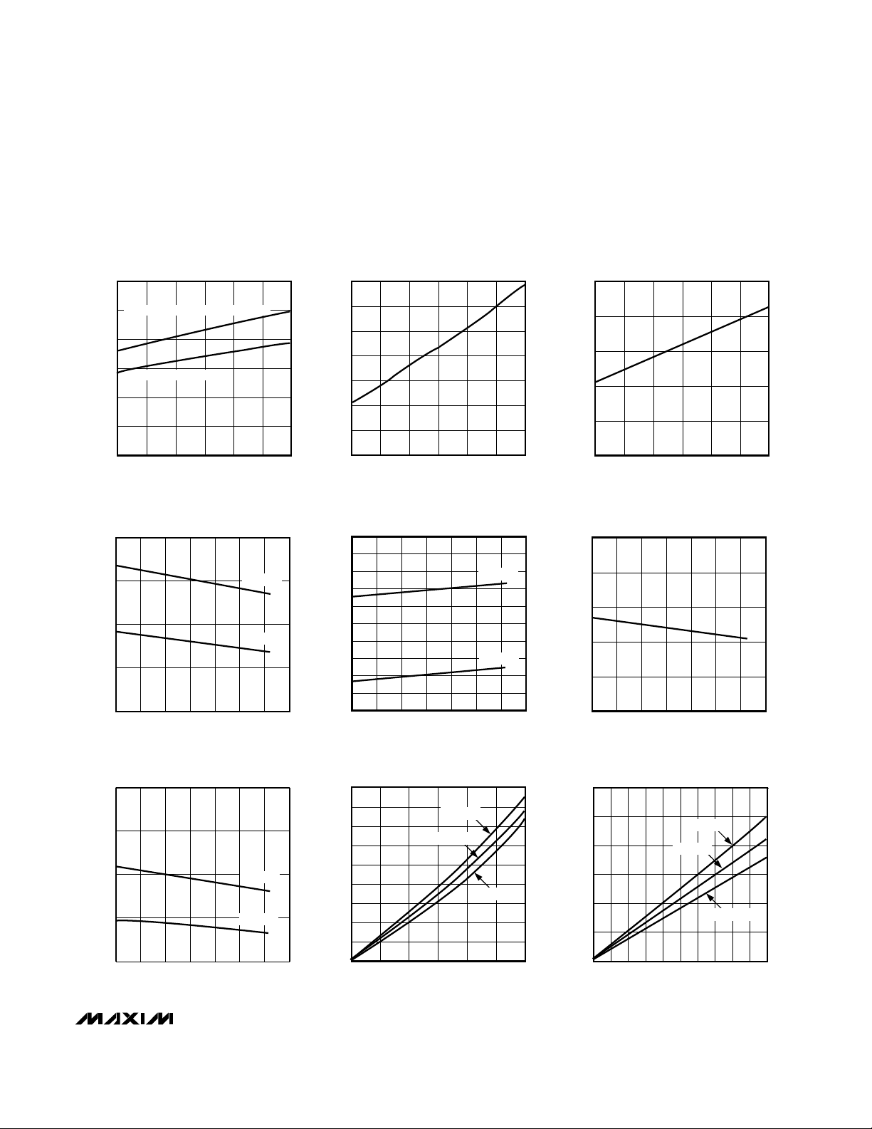
SUPPLY CURRENT
vs. SUPPLY VOLTAGE
MAX9000 TOC01
SUPPLY VOLTAGE (V)
SUPPLY CURRENT (µA)
MAX9000/MAX9001/MAX9003/MAX9004
MAX9002/MAX9005
0
1.0
0.5
2.0
1.5
3.0
2.5
3.5
2.5 3.5 4.03.0 4.5 5.0 5.5
SHUTDOWN SUPPLY CURRENT
vs. SUPPLY VOLTAGE
MAX9000 TOC02
SUPPLY VOLTAGE (V)
SHUTDOWN SUPPLY CURRENT (µA)
0
0.5
1.5
1.0
2.0
2.5
2.5 3.53.0 4.0 4.5 5.0 5.5
SHUTDOWN LOGIC THRESHOLD
vs. SUPPLY VOLTAGE
MAX9000 TOC03
SUPPLY VOLTAGE (V)
SHUTDOWN LOGIC THRESHOLD (V)
300
400
350
450
500
-40 0-20 20 40 60 80 100
MAX9000/MAX9001/MAX9003/MAX9004
SUPPLY CURRENT vs. TEMPERATURE
MAX9000 TOC04
TEMPERATURE (°C)
SUPPLY CURRENT (µA)
V
DD
= 5.5V
V
DD
= 2.5V
300
400
350
450
500
-40 0-20 20 40 60 80 100
MAX9002/MAX9005
SUPPLY CURRENT vs. TEMPERATURE
MAX9000 TOC07
TEMPERATURE (°C)
SUPPLY CURRENT (µA)
V
DD
= 5.5V
V
DD
= 2.5V
0
1.5
1.0
0.5
2.5
2.0
4.5
4.0
3.5
3.0
5.0
-40 -20 0 20 40 60 80 100
SHUTDOWN SUPPLY CURRENT
vs. TEMPERATURE
MAX9000 TOC05
TEMPERATURE (°C)
SHUTDOWN SUPPLY CURRENT (µA)
V
DD
= 5.5V
V
DD
= 2.5V
1.90
1.92
1.96
1.94
1.98
2.00
-40 0-20 20 40 60 80 100
SHUTDOWN LOGIC THRESHOLD
vs. TEMPERATURE
MAX9000 TOC06
TEMPERATURE (°C)
SHUTDOWN LOGIC THRESHOLD (V)
0
100
50
250
200
150
400
350
300
450
0 21 3 4 5 6
OP-AMP OUTPUT VOLTAGE SWING HIGH (VOH)
vs. SOURCE CURRENT
MAX9000 TOC08
SOURCE CURRENT (mA)
V
DD
- V
OH
(mV)
TA = +85°C
TA = +25°C
TA = -40°C
0
300
200
100
400
500
600
0 862 4 10 12 14 16 18 20
OP-AMP OUTPUT VOLTAGE SWING LOW (VOL)
vs. SINK CURRENT
MAX9000 TOC09
SINK CURRENT (mA)
V
OL
(mV)
TA = +85°C
TA = +25°C
TA = -40°C
__________________________________________Typical Operating Characteristics
(VDD= +5V, VSS= 0, VCM(op amp) = 0, SHDN = VDD, COUT = low, RL= ∞, TA= +25°C, unless otherwise noted.)
MAX9000–MAX9005
Low-Power, High-Speed, Single-Supply
Op Amp + Comparator + Reference ICs
6 _______________________________________________________________________________________
____________________________________Typical Operating Characteristics (continued)
(VDD= +5V, VSS= 0, VCM(op amp) = 0, SHDN = VDD, COUT = low, RL= ∞, TA= +25°C, unless otherwise noted.)
-30
-10
-20
10
0
20
30
2.5 3.5 4.03.0 4.5 5.0 5.5
CHANGE IN OP-AMP OFFSET VOLTAGE (VOS)
vs. SUPPLY VOLTAGE
MAX9000 TOC10
SUPPLY VOLTAGE (V)
CHANGE IN V
OS
(µV)
-150
-100
0
-50
50
100
-40 0-20 20 40 60 80 100
CHANGE IN OP-AMP OFFSET VOLTAGE (VOS)
vs. TEMPERATURE
MAX9000 TOC11
TEMPERATURE (°C)
CHANGE IN V
OS
(µV)
84
86
85
88
87
91
90
89
92
-40 0-20 20 40 60 80 100
OP-AMP COMMON-MODE REJECTION RATIO
vs. TEMPERATURE
MAX9000 TOC12
TEMPERATURE (°C)
CMRR (dB)
80
100
90
120
110
130
140
0 200 300100 400 500 600
OP-AMP LARGE-SIGNAL GAIN
vs. OUTPUT VOLTAGE
MAX9000 TOC13
OUTPUT VOLTAGE FROM EITHER SUPPLY (mV)
GAIN (dB)
RL = 2kΩ
RL = 10kΩ
V
DD
= 5.5V
R
L
TO GND
RL = 100kΩ
80
100
90
120
110
130
140
0 200 300100 400 500 600
OP-AMP LARGE-SIGNAL GAIN
vs. OUTPUT VOLTAGE
MAX9000 TOC16
OUTPUT VOLTAGE FROM EITHER SUPPLY (mV)
GAIN (dB)
RL = 2kΩ
RL = 10kΩ
V
DD
= 5.5V
R
L
TO V
DD
RL = 100kΩ
80
100
90
120
110
130
140
0 200 300100 400 500 600
OP-AMP LARGE-SIGNAL GAIN
vs. OUTPUT VOLTAGE
MAX9000 TOC14
OUTPUT VOLTAGE FROM EITHER SUPPLY (mV)
GAIN (dB)
V
DD
= 2.5V
R
L
TO GND
RL = 100kΩ
RL = 10kΩ
RL = 2kΩ
80
100
90
120
110
130
140
-40 0 20-20 40 60 80 100
OP-AMP LARGE-SIGNAL GAIN
vs. TEMPERATURE
MAX9000 TOC15
TEMPERATURE (°C)
GAIN (dB)
V
DD
= 5.5V
R
L
TO VDD/2
V
OUT
SWING = 0.2V TO 5.3V
RL = 100kΩ
RL = 10kΩ
RL = 1kΩ
100
120
110
130
140
0 200 300100 400 500 600
OP-AMP LARGE-SIGNAL GAIN
vs. OUTPUT VOLTAGE
MAX9000 TOC17
OUTPUT VOLTAGE FROM EITHER SUPPLY (mV)
GAIN (dB)
RL = 2kΩ
RL = 10kΩ
V
DD
= 2.7V
R
L
TO V
DD
RL = 100kΩ
80
100
90
120
110
130
140
-40 0 20-20 40 60 80 100
OP-AMP LARGE-SIGNAL GAIN
vs. TEMPERATURE
MAX9000 TOC18
TEMPERATURE (°C)
GAIN (dB)
V
DD
= 2.5V
R
L
TO VDD/2
V
OUT
SWING = 0.2V TO 2.3V
RL = 100kΩ
RL = 10kΩ
RL = 1kΩ

MAX9000–MAX9005
Low-Power, High-Speed, Single-Supply
Op Amp + Comparator + Reference ICs
_______________________________________________________________________________________
7
60
-40
100 10M10k 1M100k1k
MAX9000/MAX9001/MAX9002
OP-AMP GAIN AND PHASE
vs. FREQUENCY (NO LOAD)
0
-20
40
20
MAX9000 TOC 19
FREQUENCY (Hz)
GAIN (dB)
180
-180
-36
-72
-108
-144
108
72
144
36
0
PHASE (DEGREES)
GAIN
AV = +1000
NO LOAD
PHASE
60
-40
100 10M10k 1M100k1k
MAX9000/MAX9001/MAX9002
OP-AMP GAIN AND PHASE
vs. FREQUENCY (WITH C
LOAD
)
0
-20
40
20
MAX9000 TOC20
FREQUENCY (Hz)
GAIN (dB)
180
-180
-36
-72
-108
-144
108
72
144
36
0
PHASE (DEGREES)
AV = +1000
C
L
= 270pF
GAIN
PHASE
0
-100
100 1k 10k 100k 1M 10M
MAX9000/MAX9001/MAX9002
OP-AMP POWER-SUPPLY REJECTION
vs. FREQUENCY
-80
MAX9000 TOC21
FREQUENCY (Hz)
POWER-SUPPLY REJECTION (dB)
-60
-40
-20
AV = +1
NO LOAD
60
-40
100 1k 10k 100k 1M 10M
MAX9003/MAX9004/MAX9005
OP-AMP GAIN AND PHASE
vs. FREQUENCY (NO LOAD)
-20
MAX9000 TOC22
FREQUENCY (Hz)
GAIN (dB)
0
20
40
180
-180
-36
-72
-108
-144
108
72
144
36
0
PHASE (DEGREES)
AV = +1000
NO LOAD
GAIN
PHASE
0
10
20
30
40
50
0 400 500200 300100 600 700 800 900 1000
MAX9000/MAX9001/MAX9002
OP-AMP PERCENT OVERSHOOT
vs. LOAD CAPACITANCE
MAX9000 TOC25
C
LOAD
(pF)
OVERSHOOT (%)
AV = +1
R
L
TO VDD/2
RL = 10kΩ
RL = 1kΩ
RL = 100kΩ
60
-40
100 1k 10k 100k 1M 10M
MAX9003/MAX9004/MAX9005
OP-AMP GAIN AND PHASE
vs. FREQUENCY (WITH C
LOAD
)
-20
MAX9000 TOC23
FREQUENCY (Hz)
GAIN (dB)
0
20
40
180
-180
-36
-72
-108
-144
108
72
144
36
0
PHASE (DEGREES)
AV = +1000
C
L
= 270pF
PHASE
GAIN
0
-100
100 1k 10k 100k 1M 10M
MAX9003/MAX9004/MAX9005
OP-AMP POWER-SUPPLY REJECTION
vs. FREQUENCY
-80
MAX9000 TOC24
FREQUENCY (Hz)
POWER-SUPPLY REJECTION (dB)
-60
-40
-20
AV = +10
NO LOAD
0
10
20
30
40
50
0 400 500200 300100 600 700 800 900 1000
MAX9003/MAX9004/MAX9005
OP-AMP PERCENT OVERSHOOT
vs. LOAD CAPACITANCE
MAX9000 TOC26
C
LOAD
(pF)
OVERSHOOT (%)
AV = +10
R
L
TO VDD/2
RL = 10kΩ
RL = 1kΩ
RL = 100kΩ
1000
10
1 10 100 1k 10k 100k
OP-AMP VOLTAGE NOISE DENSITY
vs. FREQUENCY
MAX9000 TOC27
FREQUENCY (Hz)
VOLTAGE NOISE (nV/√Hz)
100
30
300
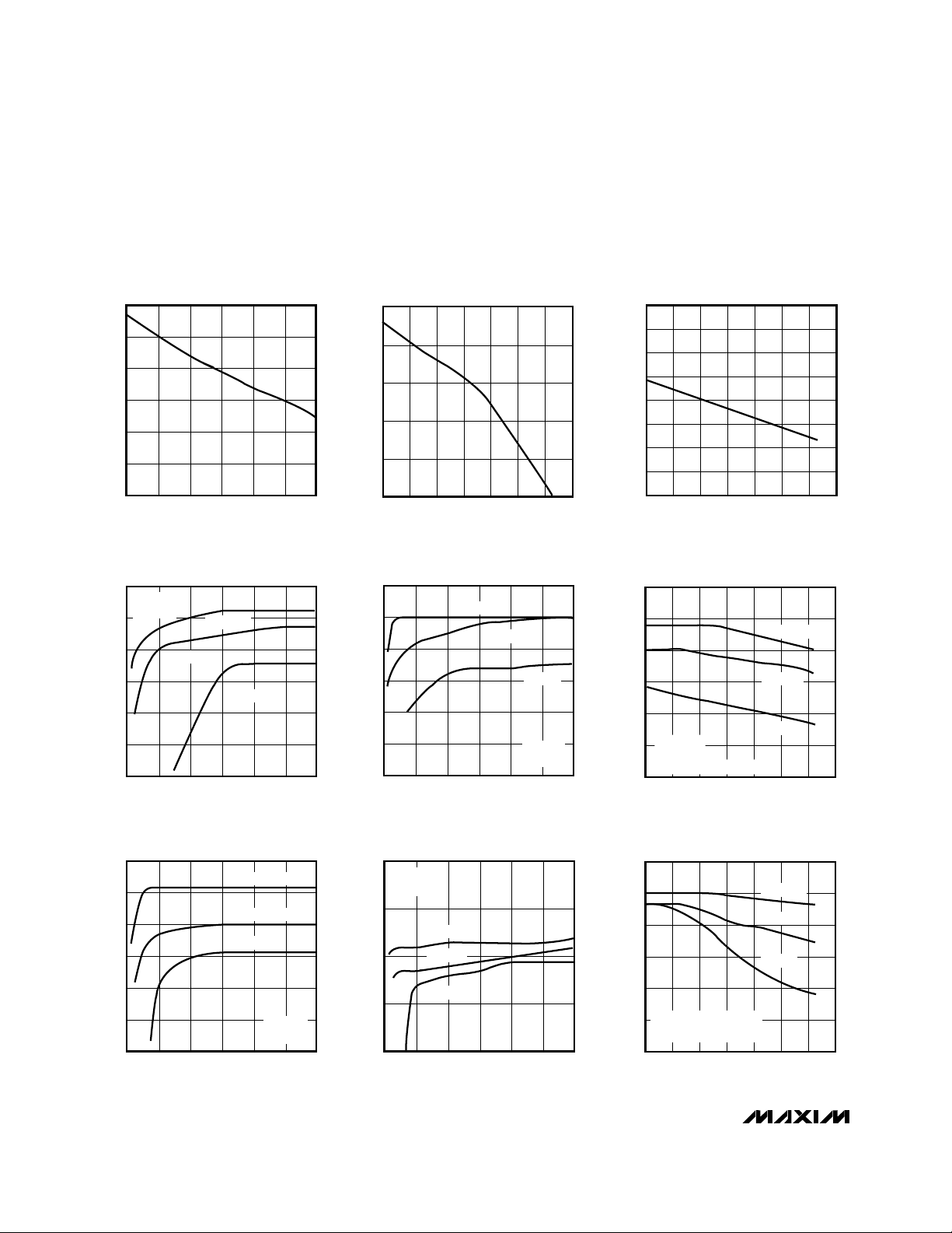
_____________________________Typical Operating Characteristics (continued)
(VDD= +5V, VSS= 0, VCM(op amp) = 0, SHDN = VDD, COUT = low, RL= ∞, TA= +25°C, unless otherwise noted.)

MAX9000–MAX9005
Low-Power, High-Speed, Single-Supply
Op Amp + Comparator + Reference ICs
8 _______________________________________________________________________________________
_____________________________Typical Operating Characteristics (continued)
(VDD= +5V, VSS= 0, VCM(op amp) = 0, SHDN = VDD, COUT = low, RL= ∞, TA= +25°C, unless otherwise noted.)
1
0.001
10 10k1k 100k
MAX9000/MAX9001/MAX9002
OP-AMP TOTAL HARMONIC DISTORTION
PLUS NOISE vs. FREQUENCY
0.01
0.1
MAX9000 TOC28
FREQUENCY (Hz)
THD + NOISE (%)
100
RL = 1kΩ
AV = +1
V
IN
= 2Vp-p
500 kHz LOWPASS FILTER
R
L
TO VDD/2
RL = 10kΩ
RL = 100kΩ
0
0.05
0.10
0.15
0.20
0.25
4.0 4.4 4.54.2 4.34.1 4.6 4.7 4.8 4.9 5.0
MAX9000/MAX9001/MAX9002
OP-AMP TOTAL HARMONIC DISTORTION
PLUS NOISE vs. V
AOUT
MAX9000 TOC29
V
AOUT
SWING (Vp-p)
THD + NOISE (%)
AV = +1
V
IN
= 10kHz SINE WAVE
500kHz LOWPASS FILTER
R
L
TO VDD/2
RL = 10kΩ
RL = 1kΩ
RL = 100kΩ
1k
0.01
100 10M10k 1M100k1k
MAX9000/MAX9001/MAX9002
OP-AMP OUTPUT IMPEDANCE vs. FREQUENCY
1
0.1
100
10
MAX9000 TOC30
FREQUENCY (Hz)
OUTPUT IMPEDANCE (Ω)
AV = +1
NO LOAD
1
0.01
10 1k 10k 100k
MAX9003/MAX9004/MAX9005
OP-AMP TOTAL HARMONIC DISTORTION
PLUS NOISE vs. FREQUENCY
0.1
MAX9000 TOC31
FREQUENCY (Hz)
THD + NOISE (%)
100
AV = +10
V
IN
= 200mVp-p
500kHz LOWPASS FILTER
R
L
TO VDD/2
RL = 1kΩ
RL = 100kΩ
RL = 10kΩ
V
IN
V
OUT
R
L
36k
4k
-200
-150
-100
-50
0
50
100
150
200
2.5 3.53.0 4.0 4.5 5.0 5.5
CHANGE IN COMPARATOR OFFSET
VOLTAGE (V
OS
) vs. SUPPLY VOLTAGE
MAX9000 TOC34
SUPPLY VOLTAGE (V)
CHANGE IN V
OS
(µV)
0
0.05
0.10
0.15
0.20
0.25
4.0 4.4 4.54.2 4.34.1 4.6 4.7 4.8 4.9 5.0
MAX9003/MAX9004/MAX9005
OP-AMP TOTAL HARMONIC DISTORTION
PLUS NOISE vs. V
AOUT
MAX9000 TOC32
V
AOUT
SWING (Vp-p)
THD + NOISE (%)
AV = +10
V
IN
= 10kHz SINE WAVE
500kHz LOWPASS FILTER
R
L
TO VDD/2
V
IN
V
OUT
R
L
36k
4k
RL = 1kΩ
RL = 100kΩ
RL = 10kΩ
10k
0.1
100 10M10k 1M100k1k
MAX9003/MAX9004/MAX9005
OP-AMP OUTPUT IMPEDANCE vs. FREQUENCY
10
1
1k
100
MAX9000 TOC33
FREQUENCY (Hz)
OUTPUT IMPEDANCE (Ω)
AV = +10
NO LOAD
-200
-150
-100
-50
0
50
100
150
200
-40 0-20 20 40 60 80 100
CHANGE IN COMPARATOR OFFSET
VOLTAGE (V
OS
) vs. TEMPERATURE
MAX9000 TOC35
TEMPERATURE (°C)
CHANGE IN V
OS
(µV)
85
87
91
89
93
95
-40 0-20 20 40 60 80 100
COMPARATOR COMMON-MODE
REJECTION RATIO (CMRR)
vs. TEMPERATURE
MAX9000 TOC36
TEMPERATURE (°C)
CMRR (dB)

MAX9000–MAX9005
Low-Power, High-Speed, Single-Supply
Op Amp + Comparator + Reference ICs
_______________________________________________________________________________________
9
2.0
2.3
2.9
2.6
3.2
3.5
-40 0-20 20 40 60 80 100
COMPARATOR HYSTERESIS
vs. TEMPERATURE
MAX9000 TOC37
TEMPERATURE (°C)
HYSTERESIS (mV)
0
300
200
100
400
500
600
0 431 2 5 6 7 8 9 10
COMPARATOR OUTPUT VOLTAGE
SWING HIGH (V
OH
) vs. SOURCE CURRENT
MAX9000 TOC38
SOURCE CURRENT (mA)
V
DD
- V
OH
(mV)
TA = +25°C
TA = +85°C
TA = -40°C
0
300
200
100
400
500
600
0 431 2 5 6 7 8 9 10
COMPARATOR OUTPUT VOLTAGE
SWING LOW (V
OL
) vs. SINK CURRENT
MAX9000 TOC39
SINK CURRENT (mA)
V
OL
(mV)
TA = +85°C
TA = +25°C
TA = -40°C
150
225
200
175
250
275
300
0 403010 20 50 60 70 80 90 100
COMPARATOR PROPAGATION DELAY
vs. INPUT OVERDRIVE
MAX9000 TOC40
INPUT OVERDRIVE (mV)
PROPAGATION DELAY (ns)
t
PD-
t
PD+
100
150
125
175
200
-40 0 20-20 40 60 80 100
COMPARATOR PROPAGATION DELAY
vs. TEMPERATURE
MAX9000 TOC43
TEMPERATURE (°C)
PROPAGATION DELAY (ns)
t
PD-
OVERDRIVE VOLTAGE = 50mV
t
PD+
100
300
200
500
400
700
600
800
0 2000 4000 6000 8000 10,000
POSITIVE COMPARATOR PROPAGATION
DELAY (t
PD+
) vs. LOAD CAPACITANCE
MAX9000 TOC41
C
LOAD
(pF)
t
PD+
(ns)
OVERDRIVE = 5mV
OVERDRIVE = 25mV
OVERDRIVE = 100mV
100
300
200
500
400
700
600
800
0 2000 4000 6000 8000 10,000
NEGATIVE COMPARATOR PROPAGATION
DELAY (t
PD-
) vs. LOAD CAPACITANCE
MAX9000 TOC42
C
LOAD
(pF)
t
PD
- (ns)
OVERDRIVE = 25mV
OVERDRIVE = 5mV
OVERDRIVE = 100mV
0
-100
1 1M10k100 100k1k10
V
REF
POWER-SUPPLY REJECTION
vs. FREQUENCY
-60
-80
-20
-40
MAX9000 TOC44
FREQUENCY (Hz)
POWER-SUPPLY REJECTION (dB)
-2.0
-1.0
-1.5
0
-0.5
0.5
1.0
-40 20 40-20 0 60 80 100
V
REF
OUTPUT VOLTAGE CHANGE
vs. TEMPERATURE
MAX9000TOC45
TEMPERATURE (°C)
V
REF
OUTPUT VOLTAGE CHANGE (mV)
_____________________________Typical Operating Characteristics (continued)
(VDD= +5V, VSS= 0, VCM(op amp) = 0, SHDN = VDD, COUT = low, RL= ∞, TA= +25°C, unless otherwise noted.)

MAX9000–MAX9005
Low-Power, High-Speed, Single-Supply
Op Amp + Comparator + Reference ICs
10 ______________________________________________________________________________________
_____________________________Typical Operating Characteristics (continued)
(VDD= +5V, VSS= 0, VCM(op amp) = 0, SHDN = VDD, COUT = low, RL= ∞, TA= +25°C, unless otherwise noted.)
-2
-1
0
1
2
3
4
-2.0 -1.0-1.5 -0.5 0 0.5 1.0 1.5 2.0
V
REF
OUTPUT VOLTAGE CHANGE
vs. LOAD CURRENT
MAX9000 TOC46
LOAD CURRENT (mA)
V
REF
OUTPUT VOLTAGE CHANGE (mV)
SINKING
SOURCING
-100
-50
0
50
100
2.5 3.53.0 4.0 4.5 5.0 5.5
V
REF
OUTPUT VOLTAGE CHANGE
vs. SUPPLY VOLTAGE
MAX9000 TOC47
SUPPLY VOLTAGE (V)
V
REF
OUTPUT VOLTAGE CHANGE (µV)
50µs/div
V
REF
LOAD-TRANSIENT RESPONSE
I
OUT
2mA/div
V
REF
200mV/div
+1mA
-1mA
MAX9000-TOC48
5µs/div
V
REF
LINE-TRANSIENT RESPONSE
V
DD
500mV/div
V
REF
100mV/div
5.0V
4.5V
MAX9000-TOC49
500ns/div
MAX9000/MAX9001/MAX9002
OP-AMP SMALL-SIGNAL TRANSIENT RESPONSE
V
IN
50mV/div
V
OUT
50mV/div
MAX9000-TOC52
AV = +1
NO LOAD
1sec/div
V
REF
0.1Hz to 10Hz VOLTAGE NOISE
5µV/div
MAX9000-TOC50
100ns/div
-50mW
+50mW
COMPARATOR PROPAGATION DELAY
V
IN+
50mV/div
V
OUT
2V/div
VIN- = GND
NO LOAD
t
PD+
MAX9000-TOC51
t
PD-
1µs/div
MAX9000/MAX9001/MAX9002
OP-AMP SMALL-SIGNAL TRANSIENT
RESPONSE WITH C
LOAD
V
IN
50mV/div
V
OUT
50mV/div
MAX9000-TOC53
AV = +1
C
L
= 270pF
500ns/div
MAX9003/MAX9004/MAX9005
OP-AMP SMALL-SIGNAL TRANSIENT RESPONSE
V
IN
10mV/div
V
OUT
50mV/div
MAX9000-TOC54
AV = +10
NO LOAD

MAX9000–MAX9005
Low-Power, High-Speed, Single-Supply
Op Amp + Comparator + Reference ICs
______________________________________________________________________________________ 11
_____________________________Typical Operating Characteristics (continued)
(VDD= +5V, VSS= 0, VCM(op amp) = 0, SHDN = VDD, COUT = low, RL= ∞, TA= +25°C, unless otherwise noted.)
Pin Description
Shutdown Logic Input—— 21
MAX9000/
MAX9003
FUNCTION
MAX9002/
MAX9005
SHDN
32 AOUT Op-Amp Output11
43 AIN54 AIN+ Noninverting Op-Amp Input33
Inverting Op-Amp Input22
65 V
SS
96 REF Internal Reference Output—5
107 CIN118 CIN+ Noninverting Comparator Input66
Inverting Comparator Input5—
Negative Supply or Ground44
129 COUT Comparator Output77
1310 V
DD
1, 7, 8, 14— N.C. No Connection. Not internally connected.——
Positive Supply88
NAME
PIN
MAX9001/MAX9004
10 µMAX 14 SO
MAX9003/MAX9004/MAX9005
V
10mV/div
V
OUT
50mV/div
OP-AMP SMALL-SIGNAL TRANSIENT
RESPONSE WITH C
IN
LOAD
1µs/div
AV = +1
C
= 270pF
L
MAX9000/MAX9001/MAX9002
OP-AMP LARGE-SIGNAL TRANSIENT RESPONSE
V
IN
5V/div
MAX9000-TOC55
4V
V
OUT
1V/div
0V
2
µs/div
AV = +1
NO LOAD
MAX9000-TOC56
0.5V/div
MAX9003/MAX9004/MAX9005
OP-AMP LARGE-SIGNAL TRANSIENT RESPONSE
AV = +10
NO LOAD
V
OUT
1V/div
V
IN
5V
0V
500ns/div
MAX9000-TOC57

MAX9000–MAX9005
Low-Power, High-Speed, Single-Supply
Op Amp + Comparator + Reference ICs
12 ______________________________________________________________________________________
_______________Detailed Description
The MAX9001–MAX9005 are combinations of a highspeed operational amplifier, a 185ns comparator, and a
1%-accurate, 8ppm/°C, 1.230V reference. The devices
are offered in space-saving 8-pin and 10-pin µMAX packages. The comparator’s inverting input is internally connected to the reference output in the MAX9000/MAX9003.
The MAX9002/MAX9005 do not have an internal reference, but the inverting input of the comparator is available externally. The MAX9001/MAX9004 include both the
inverting input and the reference output. The MAX9000/
MAX9001/MAX9003/MAX9004 typically consume only
410µA of quiescent current, while the MAX9002/
MAX9004 typically consume 340µA. These low-power,
Rail-to-Rail devices provide excellent AC and DC performance and are ideally suited to operate from a single
supply. The MAX9001/MAX9004 feature a shutdown
mode that sets the outputs in a high-impedance state and
reduces the supply current to 2µA, making these devices
ideal for portable and battery-powered systems.
Op Amp
The op amps in the MAX9000/MAX9001/MAX9002 are
unity-gain stable with a gain-bandwidth product of
1.25MHz and a slew rate of 0.85V/µs. The amplifiers in
the MAX9003/MAX9004/MAX9005 are stable at closedloop gains greater than or equal to 10V/V, with a gainbandwidth product of 8MHz and a slew rate of 6.0V/µs.
The common-mode input voltage range extends from
150mV below the negative rail to within 1.2V of the positive rail. The amplifier output does not undergo phase
reversal when the common-mode input range is
exceeded, and the input impedance is relatively constant for input voltages within both supply rails. The
MOS differential inputs of the amplifiers feature
extremely high input impedance and ultra-low input
bias currents. The CMOS output stage achieves true
rail-to-rail operation; the outputs swing to within a few
millivolts of the supply rails, thus extending the dynamic
range. A proprietary design achieves high open-loop
gain, enabling these devices to operate at low quiescent currents yet maintain excellent DC and AC characteristics under various load conditions. These
devices have been designed to maintain low offset voltage over the entire operating-temperature, commonmode, and supply-voltage ranges.
MAX9000
MAX9003
OP AMP
COMP
REF
1
2
3
4
8
7
6
5
AOUT
AIN-
AIN+
V
SS
V
DD
COUT
CIN+
REF
MAX9002
MAX9005
OP AMP
COMP
1
2
3
4
8
7
6
5
AOUT
AIN-
AIN+
V
SS
V
DD
COUT
CIN+
CIN-
MAX9001
MAX9004
OP AMP
COMP
REF
4M
3
4
5
6
12
11
10
9
AOUT
AIN-
AIN+
V
SS
V
DD
2 13SHDN V
DD
CIN+
CIN-
REF
NORMAL/SHUTDOWN CONTROL
Figure 1. MAX9000–MAX90005 Functional Diagrams

Comparator
The common-mode input range extends from 150mV
below the negative rail to within 1.1V of the positive rail.
The bipolar differential inputs of the comparator feature
high input impedance and low input bias currents. The
comparators are designed to maintain low offset voltage over the entire operating-temperature, commonmode, and supply-voltage ranges. In the MAX9000/
MAX9003, the comparator’s inverting input is internally
connected to the reference output.
The CMOS output stage achieves true rail-to-rail operation; the outputs swing to within a few millivolts of the
supply rails. The comparator’s propagation delay is
185ns and is a function of the overdrive (see
Typical
Operating Characteristics
). TTL/CMOS compatibility is
maintained even with a ±4mA output load. A proprietary design of the output stage substantially reduces
the cross-conduction current during output transitions,
thereby minimizing power-supply glitches typical of
most comparators. In addition, the comparator’s ±2mV
of built-in hysteresis provides noise immunity and prevents unstable outputs even with slow-moving input
signals.
Voltage Reference
The 1%-accurate, precision 1.230V internal bandgap
reference in the MAX9000/MAX9001/MAX9003/
MAX9004 achieves an 8ppm/°C temperature coefficient
(tempco). The reference can sink or source 1mA of load
current with excellent load regulation. The output typically changes only 60µV for a 3V change in input voltage
(line regulation). The reference is stable for capacitive
loads up to 100nF.
Applications Information
The MAX9000–MAX9005 offer excellent performance
and low power consumption, and are available in
space-saving µMAX packages. The following section
provides some practical application guidelines.
Bypassing and Layout
The MAX9000–MAX9005 operate from a +2.5V to +5.5V
single supply or from ±1.25V to ±2.75V dual supplies.
(In the MAX9000/MAX9001/MAX9003/MAX9004, the
reference voltage is referred to as VSS.). For singlesupply operation, bypass the power supply with a
0.1µF capacitor. For dual supplies, bypass each supply
to ground. Bypass with capacitors as close as possible
to the device to minimize lead inductance and noise.
Use a low-inductance ground plane if possible. A printed circuit board with a ground plane is recommended.
Avoid using wire-wrap boards, breadboards, or IC
sockets. For heavy loads at the comparator’s and/or
amplifier’s output, add a 1µF to 10µF power-supply
bypass capacitor.
The device has a high degree of isolation between the
various blocks. To maintain isolation, careful layout is
required. Take special precautions to avoid crossing
signal traces, especially from the outputs to the inputs.
For sensitive applications, shielding might be required.
In addition, stray capacitance may affect the stability
and frequency response of the amplifier. Decrease
stray capacitance by minimizing lead lengths in the
board layout, as well as placing external components
as close to the device as possible.
Op-Amp Frequency Stability
Driving large capacitive loads can cause instability in
most low-power, rail-to-rail output amplifiers. These
amplifiers are stable with capacitive loads up to 250pF in
their minimum gain configuration. Stability with higher
capacitive loads can be improved by adding an isolation
resistor in series with the op-amp output, as shown in
Figure 2. This resistor improves the circuit’s phase margin by isolating the load capacitor from the amplifier’s
output. Figures 3 and 4 show the response of the amplifier with and without an isolation resistor, respectively.
The total capacitance at the op amp’s inputs (input
capacitance + stray capacitance) along with large-value
feedback resistors can cause additional poles within the
amplifier’s bandwidth, thus degrading the phase margin.
To compensate for this effect, place a 2pF to 10pF
capacitor across the feedback resistor, as shown in
Figure 5.
MAX9000–MAX9005
Low-Power, High-Speed, Single-Supply
Op Amp + Comparator + Reference ICs
______________________________________________________________________________________ 13
MAX9000
MAX9001
MAX9002
MAX9003
MAX9004
MAX9005
R
S
R
R
R
S
C
LOAD
C
LOAD
Figure 2. Isolation Resistors to Drive Capacitive Loads

MAX9000–MAX9005
Reference Bypassing
While the internal reference is stable with capacitive
loads up to 100nF, it does not require an output capacitor for stability. However, in applications where the load
or the supply could experience large step changes, an
output capacitor reduces the amount of overshoot and
improves the circuit’s transient response.
Comparator Input Stage
The comparator’s input bias current is typically 8nA. To
reduce the offset error caused by the bias current flowing through the external source impedance, match the
effective impedance seen by each input. High source
impedance together with the comparator’s input capacitance can increase the propagation delay through the
comparator. The outputs do not undergo phase reversal when the input common-mode range is exceeded,
and the input impedance is relatively constant for input
voltages within both supply rails.
Comparator Hysteresis
Built-in ±2mV hysteresis improves the comparator’s
noise immunity. It prevents unstable outputs with slowmoving or noisy input signals. If additional hysteresis is
required, add positive feedback as shown in Figure 6.
This configuration increases the hysteresis band to
desired levels, but also increases power consumption
and slows down the output response.
Low-Power, High-Speed, Single-Supply
Op Amp + Comparator + Reference ICs
14 ______________________________________________________________________________________
2µs/div
V
IN
50mV/
div
V
OUT
50mV/
div
MAX9000-FIG03
Figure 3. MAX9000/MAX9001/MAX9002 Op-Amp Small-Signal
Transient Response with Capacitive Load (C
L
= 510pF) and
Isolation Resistor (R
ISO
= 91Ω)
Figure 5. Compensation for Input Capacitance
R1
R2
2pF TO 10pF
AOUT
AIN+
Figure 4. MAX9000/MAX9001/MAX9002 Op-Amp Small-Signal
Transient Response with Capacitive Load (C
L
= 510pF) and
No Isolation Resistor
REF
R2
R1
COUT
V
IN
Figure 6. External Hysteresis
V
IN
50mV/
div
V
OUT
50mV/
div
VDD = +1
C
= 510pF
L
2µs/div
MAX9000-FIG04

To add hysteresis, use the following procedure:
Step 1: The device’s input bias current can be as high
as 80nA. To minimize error due to the input bias,
choose a value for R2 of 100kΩ (V
REF
/ R2), which
allows a current of 12.33µA at the upper trip point.
Step 2: Choose the width of the hysteresis band. In this
example, choose 20mV for the added external hysteresis (V
EHYST
= 20mV). Total hysteresis = V
EHYST
+
V
IHYST
= 24mV.
R1 = R2 (V
EHYST
- 2V
IHYST
) / (VDD+ 2V
IHYST
)
where
IHYST
is the device’s internal hysteresis.
Step 3: Determine R1. If VDD= 5V, then R1 = 319Ω.
Step 4: Check the hysteresis trip points. The following
equation represents the upper trip point (V
IN(H)
):
V
IN(H)
= [(R1 + R2) / R2] (V
REF
+ V
IHYST
) = 1.238V
The lower trip point is 24mV lower than upper trip point.
V
IN(L
)
= 1.238V - 0.024V = 1.214V.
Comparator Propagation Delay
The comparator’s propagation delay is a function of the
input overdrive voltage. Overdrive voltage is measured
from beyond the edge of the offset and hysteresisdetermined trip points (see
Typical Operating
Characteristics
for a graph of Propagation Delay vs.
Input Overdrive). High source impedance coupled with
the comparator’s input capacitance increases the propagation delay. Large capacitive loads also increase the
propagation delay.
Shutdown
(
SSHHDDNN
)
Shutdown is active-low enabled. The SHDN input for
the MAX9001/MAX9004 can be taken above the posi-
tive supply without an increase in the SHDN input current, allowing them to be driven from independent logic
circuits powered from a different supply voltage.
However, the logic threshold voltage requirements
must be met for proper operation. If SHDN is left
unconnected, the device defaults to the enabled mode
through an internal 4MΩ pull-up to V
DD
. If SHDN is to
be left unconnected, take proper care to ensure that no
signals are coupled to this pin, as this may cause false
triggering.
In shutdown mode, all outputs are set to a high-impedance state and the supply current reduces to 2µA.
Enable times for the op amp, comparator, and reference are 2µs, 100ns, and 16µs, respectively. Shutdown
delay times for the op amp, comparator, and reference
are 200ns, 100ns, and 1µs, respectively (Figure 7).
________________Application Circuits
Radio Receiver for Alarms
and Detectors
Figure 8’s circuit is useful as a front end for RF alarms.
An unshielded inductor is used with capacitors C1A,
C1B, and C1C in a resonant circuit to provide frequency selectivity. The op amp from a MAX9003 amplifies
the signal received. The comparator improves noise
immunity, provides a signal-strength threshold, and
translates the received signal into a pulse train. The
tuned LC circuit in Figure 8 is set for 300kHz. The layout and routing of components for the amplifier should
be tight to minimize 60Hz interference and crosstalk
from the comparator. Metal shielding is recommended
to prevent RFI from the comparator or digital circuitry
from exciting the receiving antenna. The transmitting
MAX9000–MAX9005
Low-Power, High-Speed, Single-Supply
Op Amp + Comparator + Reference ICs
______________________________________________________________________________________ 15
5µs/div
SHDN
5V/div
AOUT
2V/div
COUT
5V/div
VREF
1V/div
MAX9000-FIG07
AV = +1V/V, C
AIN+
= 2.5V, C
CIN+
= 2.5V
Figure 7. Enable/Disable Response of Op Amp, Comparator,
and Reference to
SHDN
REF
0.1µF
0.1µF
L1
33µH
C1A
390pF
1
(2π f
C
)
2
C1B
0.01nF
C1C
10M
5.1M
9.1k
10k
1.230V
20k
V
CC
= 5V
COMP
ANTENNA
AMP
LAYOUT-SENSITIVE AREA,
METAL RFI SHIELDING ADVISED
MAX9003
L1 x C1 =
50-100pF
Figure 8. Radio Receiver Application

MAX9000–MAX9005
antenna can be long parallel wires spaced about 7.2cm
apart, with equal but opposite currents. Radio waves
from this antenna are detectable when the receiver is
brought within close proximity, but cancel out at greater
distances.
Infrared Receiver Front End for
Remote Controls and Data Links
The circuit in Figure 9 uses the MAX9003 as a PIN photodiode preamplifier and discriminator for an infrared
receiver. The op amp is configured as a Delyiannisnoise and eliminates low-frequency interference from
sunlight, fluorescent lights, etc. This circuit is applicable for TV remote controls and low-frequency data links
up to 200kbps. Carrier frequencies are limited to
around 100kHz, as in the example circuit. Component
layout and routing for the amplifier should be tight to
reduce stray capacitance, 60Hz interference, and RFI
from the comparator. Crosstalk from comparator edges
distorts the amplifier signal. To minimize this effect, add
a lowpass RC filter to the connection from the reference
to the op amp’s noninverting input.
Signal Conditioning
For incoming signals that require filtering, the internal
amplifier provides an opportunity to create an active filter. This may be required for relatively high-speed signals that require adequate filtering of high-speed
carrier frequencies, harmonics, and external noise. In
addition, the amplifier can be used to amplify the signal
prior to digitizing it through the comparator to improve
the comparator’s overall output response and improve
its noise immunity.
Low-Power, High-Speed, Single-Supply
Op Amp + Comparator + Reference ICs
16 ______________________________________________________________________________________
REF
0.1µF
0.1µF
1
2π f
C
100k
1.230V
V
CC
= 5V
COMP
AMP
C2
15pF, 5%
100kHz,
5Vp-p
C1
150pF,
5%
NEC
PH302B
NEC
SE307-C
51Ω
R1
A
49.9k
1%
R1
B
4.99k
1%
R2
100k,
1%
LAYOUT-SENSITIVE AREA
MAX9003
R1 x C1 = R2 x C2 =
4.99k
Figure 9. Infrared Receiver Application

MAX9000–MAX9005
Low-Power, High-Speed, Single-Supply
Op Amp + Comparator + Reference ICs
______________________________________________________________________________________ 17
Pin Configurations
CIN+
REF (CIN-)V
SS
( ) ARE FOR THE MAX9002/MAX9005.
1
2
87V
DD
COUTAIN-
AIN+
AOUT
SO/µMAX
TOP VIEW
3
4
6
5
MAX9000
MAX9002
MAX9003
MAX9005
1
2
3
4
5
10
9
8
7
6
V
DD
COUT
CIN+
CIN-AIN+
AIN-
AOUT
SHDN
MAX9001
MAX9004
µMAX
SO
REFV
SS
14
13
12
11
10
9
8
1
2
3
4
5
6
7
N.C.
V
DD
COUT
CIN+AIN-
AOUT
SHDN
N.C.
MAX9001
MAX9004
CINREF
N.C.N.C.
V
SS
AIN+
Typical Operating Circuit
V
DD
MAX9000
MAX9003
COMP
REF
1.230V
V
SS
COUT
0.1µF
INPUT
1M
AIN+
OP AMP
AIN-
AOUT
CIN+
R2
R1
REF

MAX9000–MAX9005
Low-Power, High-Speed, Single-Supply
Op Amp + Comparator + Reference ICs
18 ______________________________________________________________________________________
Ordering Information (continued) Chip Information
TRANSISTOR COUNT: 283
PART TEMP. RANGE PIN-PACKAGE
MAX9002EUA
MAX9002ESA -40°C to +85°C
-40°C to +85°C 8 µMAX
8 SO
MAX9003EUA
MAX9003ESA
MAX9004EUB
MAX9004ESD
-40°C to +85°C
-40°C to +85°C 8 µMAX
8 SO
-40°C to +85°C
-40°C to +85°C 10 µMAX
14 SO
MAX9005EUA
MAX9005ESA -40°C to +85°C
-40°C to +85°C 8 µMAX
8 SO
Package Information
8LUMAXD.EPS

MAX9000–MAX9005
Low-Power, High-Speed, Single-Supply
Op Amp + Comparator + Reference ICs
______________________________________________________________________________________ 19
Package Information (continued)
10LUMAXB.EPS

MAX9000–MAX9005
Low-Power, High-Speed, Single-Supply
Op Amp + Comparator + Reference ICs
Maxim cannot assume responsibility for use of any circuitry other than circuitry entirely embodied in a Maxim product. No circuit patent licenses are
implied. Maxim reserves the right to change the circuitry and specifications without notice at any time.
20
____________________Maxim Integrated Products, 120 San Gabriel Drive, Sunnyvale, CA 94086 408-737-7600
© 1998 Maxim Integrated Products Printed USA is a registered trademark of Maxim Integrated Products.
Package Information (continued)
SOICN.EPS
 Loading...