Maxim MAX895LESA, MAX894LC-D, MAX894LESA, MAX895LC-D Datasheet

19-1153; Rev 0; 10/96
Dual, Current-Limited, High-Side P-Channel
Switches with Thermal Shutdown
_______________General Description
The MAX894L/MAX895L smart, dual, low-voltage,
P-channel, MOSFET power switches are intended for
high-side load-switching applications. These switches
operate with inputs from +2.7V to +5.5V, making them
ideal for both 3V and 5V systems. Internal currentlimiting circuitry protects the input supply against
overload. Thermal-overload protection limits power dissipation and junction temperature.
The MAX894L/MAX895L’s maximum current limits are
500mA and 250mA, respectively. The current limit
through the switches is programmed with resistors from
SET A/SET B to ground. When the switches are on, the
quiescent supply current is a low 16µA. When the
switches are off, the supply current decreases to 0.1µA.
The MAX894L/MAX895L are available in an 8-pin SO
package.
________________________Applications
PCMCIA Slots
Access Bus Slots
Portable Equipment
____________________________Features
♦ +2.7V to +5.5V Input Range
♦ Programmable Current Limits
♦ Low Supply Current:
16µA I
at VIN= 3.3V
Q
0.1µA with Switch Off
♦ Thermal Shutdown
______________Ordering Information
PART*
MAX894LC/D
MAX894LESA -40°C to +85°C
MAX895LC/D
MAX895LESA -40°C to +85°C 8 SO 250mA
*
To order these units in tape and reel, add (-T) to the end of the
part number.
**
Dice are tested at TA= +25°C.
TEMP.
RANGE
0°C to +70°C
0°C to +70°C Dice** 250mA
PIN-
PACKAGE
Dice**
8 SO
CURRENT
LIMIT
500mA
500mA
MAX894L/MAX895L
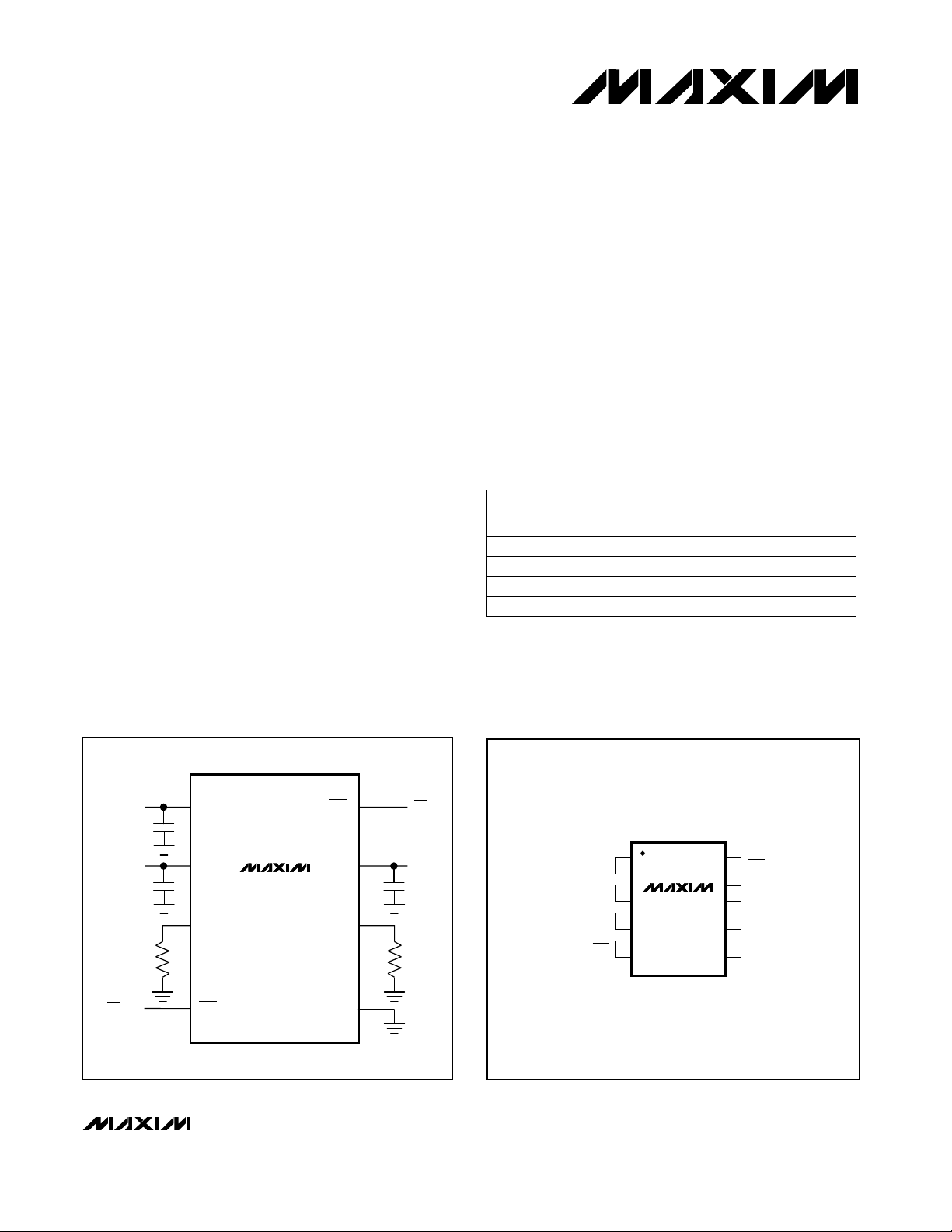
__________Typical Operating Circuit
OUTPUT A
0.1µF
OUTPUT B
0.1µF1µF
R
SET A
ON/OFF
OUT A
OUT B
MAX894L
MAX895L
SET A
ONA
________________________________________________________________
ONB
SET B
GND
ON/OFF
IN
INPUT
R
SET B
__________________Pin Configuration
TOP VIEW
OUT A
OUT B
SET A
ONA
1
2
MAX894L
MAX895L
3
4
SO
Maxim Integrated Products
ONB
8
IN
7
SET B
6
GND
5
1
For free samples & the latest literature: http://www.maxim-ic.com, or phone 1-800-998-8800

Dual, Current-Limited, High-Side P-Channel
Switches with Thermal Shutdown
ABSOLUTE MAXIMUM RATINGS
IN to GND...................................................................-0.3V to 6V
ONA, ONB to GND.....................................................-0.3V to 6V
SET A, SET B, OUT A, OUT B to GND ........-0.3V to (V
Maximum Continuous Switch Current
MAX894L..........................................................................0.75A
MAX895L........................................................................0.375A
Stresses beyond those listed under “Absolute Maximum Ratings” may cause permanent damage to the device. These are stress ratings only, and functional
operation of the device at these or any other conditions beyond those indicated in the operational sections of the specifications is not implied. Exposure to
absolute maximum rating conditions for extended periods may affect device reliability.
+ 0.3V)
IN
Continuous Power Dissipation (T
SO (derate 5.88mW/°C above +70°C) .......................471mW
Operating Temperature Range
MAX89_LESA .................................................-40°C to +85°C
Storage Temperature Range...............................-65°C to+150°C
Lead Temperature (soldering, 10sec)..............................+300°C
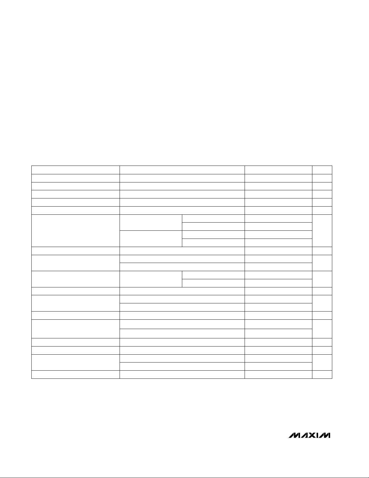
ELECTRICAL CHARACTERISTICS
(VIN= 3V, TA= 0°C to +85°C, unless otherwise noted. Typical values are at TA= +25°C.)
CONDITION
Quiescent Current
MAX894L/MAX895L
On-Resistance
Maximum Output Current
I
to I
OUT
ONA, ONB Input Low Voltage
ONA, ONB Input High Voltage
ONA, ONB Input Leakage
I
SETA,ISETB
Turn-On Time
Turn-Off Time 0.8 1.2 20
Note 1: Tested with I
Current Ratio
SET
Bias Current
= 50mA for the MAX894L and 25mA for the MAX895L, and V
OUT
VIN= 5V, ONA = ONB = GND, I
ONA = ONB = IN, VIN= V
ONA = ONB = IN, VIN= 5.5V, V
Rising edge, 1% hysteresis
VIN= 4.5V
VIN= 3.0V
V
required to turn the switch off (Note 1)
SET
MAX894L
MAX895L
= 1.6V to 2.8V
OUT
VIN= 2.7V to 5.5V
VIN= 2.7V to 3.6V
VIN= 4.5V to 5.5V
V
= V
ONA
V
SET A
V
SET B
20% current overdrive, VCC= 5V
VIN= 5V, I
VIN= 3V, I
= 5.5V
ONB
= 1.24V, ONA = 0, ONB = VIN, I
= 1.24V, ONB = 0, ONA = VIN, I
= 250mA (MAX894L), 125mA (MAX895L) 100 200
OUT
= 250mA (MAX894L), 125mA (MAX895L) 150
OUT
OUT A
MAX894L
MAX895L
MAX894L
MAX895L
MAX894L, I
MAX895L, I
OUT A
= V
OUT A
= I
OUT B
= V
OUT
OUT
OUT A
OUT B
OUT B
= 5.5V
OUT B
= 250mA
= 125mA
= 0
= 0
= 0
= 0
raised until VIN- V
SET
= +70°C)
A
18 30
0.03 1Off-Supply Current
0.04 3Off-Switch Current
120 225
250 420
150 300
300 500
500
250
945 1085 1270
910 1050 1235
2.0
2.4
0.01 1
0.5 3
0.5 3
5Slow-Current-Loop Response Time
2Fast-Current-Loop Response Time
≥ 0.8V.
OUT
UNITSMIN TYP MAXPARAMETER
V2.7 5.5Operating Voltage
µA
µA
µA
V2.0 2.4 2.6Undervoltage Lockout
mΩ
V1.178 1.240 1.302Current-Limit-Amplifier Threshold
mA
A/AV
V0.8
V
µA
µA
µs
µs
µs
µs
2 _______________________________________________________________________________________

Dual, Current-Limited, High-Side P-Channel
Switches with Thermal Shutdown
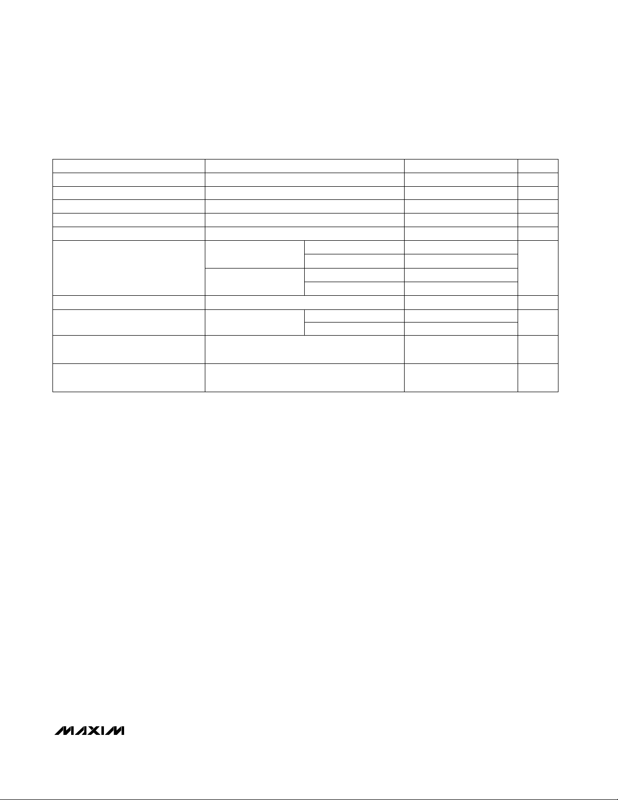
ELECTRICAL CHARACTERISTICS (Note 2)
(VIN= 3V, TA= -40°C to +85°C, unless otherwise noted. Typical values are at TA= +25°C.)
CONDITION
Quiescent Current
On-Resistance
I
to I
OUT
Note 2: Specifications to -40°C are guaranteed by design, not production tested.
Current Ratio
SET
VIN= 5V, ONA = ONB = GND, I
ONA = ONB = IN, VIN= V
ONA = ONB = IN, VIN= 5.5V, V
Rising edge, 1% hysteresis
VIN= 4.5V
VIN= 3.0V
V
required to turn the switch off (Note 1)
SET_
V
= 1.24V,
SET
V
= 1.6V to 2.8V
OUT
VIN= 5V
OUT A
MAX894L
MAX895L
MAX894L
MAX895L
MAX894L, I
MAX895L, I
OUT A
= V
OUT A
= I
OUT B
= V
OUT
OUT
= 0
OUT B
= 5.5V
= 0
OUT B
= 250mA
= 125mA 880 1315
50
2.2Off-Supply Current
8Off-Switch Current
250
420
300
500
910 1360
200Turn-On Time
0.25 20Turn-Off Time
MAX894L/MAX895L
UNITSMIN TYP MAXPARAMETER
V3.0 5.5Operating Voltage
µA
µA
µA
V2.0 2.9Undervoltage Lockout
mΩ
V1.14 1.34Current-Limit-Amplifier Threshold
A/A
µs
µs
_______________________________________________________________________________________ 3
 Loading...