

General Description
The MAX890L smart, low-voltage, P-channel, MOSFET
power switch is intended for high-side load-switching
applications. This switch operates with inputs from 2.7V
to 5.5V, making it ideal for both 3V and 5V systems.
Internal current-limiting circuitry protects the input supply against overload. Thermal-overload protection limits
power dissipation and junction temperatures.
The MAX890L’s maximum current limit is 1A. The current limit through the switch is programmed with a
resistor from SET to ground. The quiescent supply current is a low 10µA. When the switch is off, the supply
current decreases to 0.1µA.
The MAX890L is available in an 8-pin SO package.
________________________Applications
PCMCIA Slots
Access Bus Slots
Portable Equipment
____________________________Features
♦ 2.7V to 5.5V Input Range
♦ Programmable Current Limit
♦ Low Quiescent Current
10µA (typ) at V
IN
= 3.3V
0.1µA (typ) with Switch Off
♦ Thermal Shutdown
♦ FAULT Indicator Output
♦ 0.09Ω (typ) On-Resistance
MAX890L
1A, Current-Limited, High-Side
P-Channel Switch with Thermal Shutdown
________________________________________________________________
Maxim Integrated Products
1
1
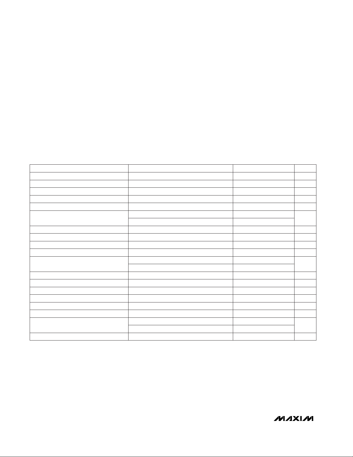
2
8
7
FAULT
OUT
OUT
SET
IN
IN
ON
GND
MAX890L
SO
TOP VIEW
3
4
6
5
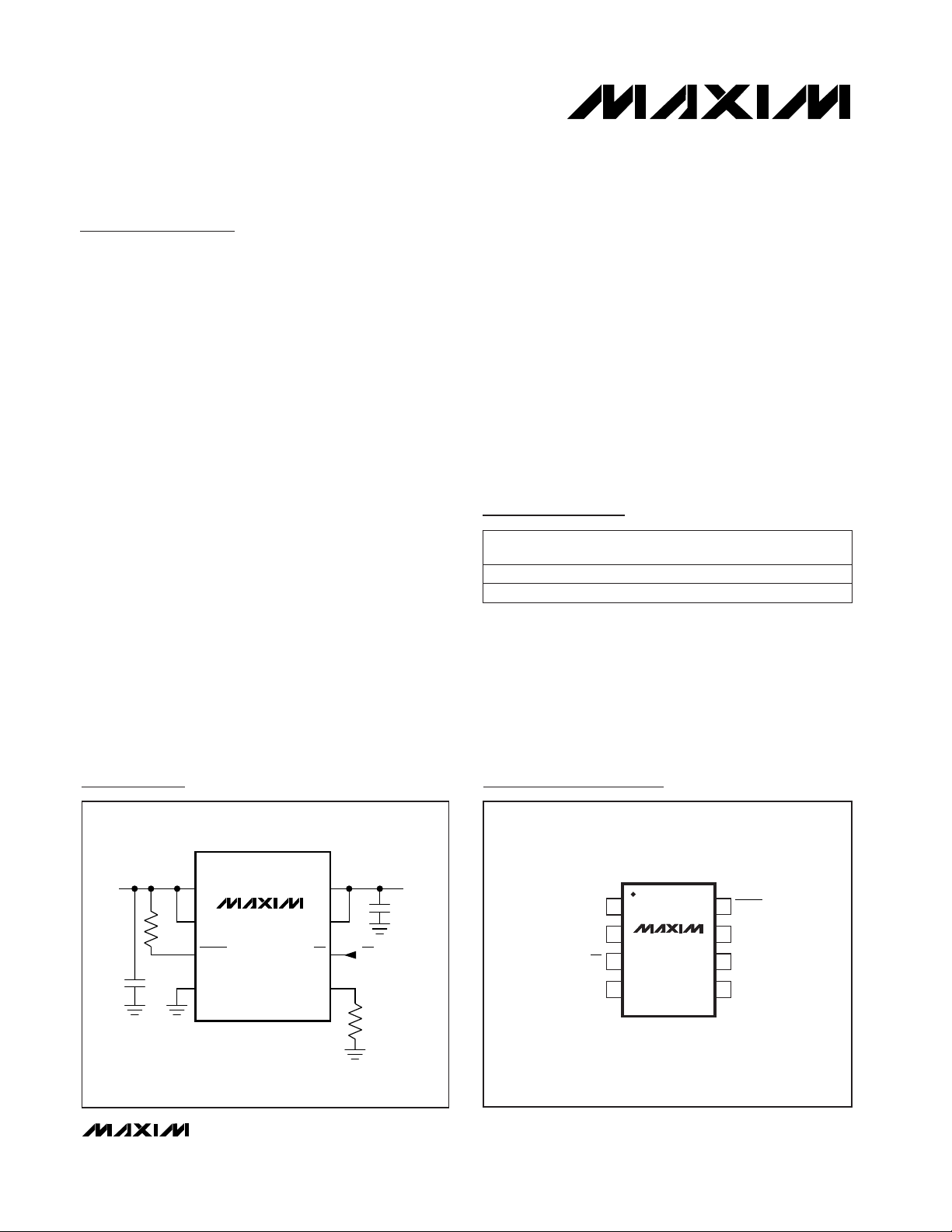
Pin Configuration
MAX890L
1µF
0.1µF
100kΩ
IN OUTPUTOUTINPUT
IN OUT
FAULT ON
ON/OFF
R
SET
GND SET
Typical Operating Circuit
19-1146; Rev 2; 11/98
PART*
MAX890LC/D 0°C to +70°C
TEMP.
RANGE
PIN-
PACKAGE
Dice**
Ordering Information
*
To order this unit in tape and reel, add (-T) to the end of the part
number.
**
Dice are tested at TA= +25°C.
CURRENT
LIMIT
1A
1AMAX890LESA -40° C t o +85°C 8 SO
For free samples & the latest literature: http://www.maxim-ic.com, or phone 1-800-998-8800.
For small orders, phone 1-800-835-8769.
MAX890L
1A, Current-Limited, High-Side
P-Channel Switch with Thermal Shutdown
2 _______________________________________________________________________________________
ABSOLUTE MAXIMUM RATINGS
ELECTRICAL CHARACTERISTICS
(VIN= 3V, TA= 0°C to +85°C, unless otherwise noted. Typical values are at TA= +25°C.)
Stresses beyond those listed under “Absolute Maximum Ratings” may cause permanent damage to the device. These are stress ratings only, and functional
operation of the device at these or any other conditions beyond those indicated in the operational sections of the specifications is not implied. Exposure to
absolute maximum rating conditions for extended periods may affect device reliability.
IN to GND ..................................................................-0.3V to 6V
ON, FAULT to GND ....................................................-0.3V to 6V
SET, OUT to GND ......................................-0.3V to (V
IN
+ 0.3V)
Maximum Continuous Switch Current ..................................1.5A
Continuous Power Dissipation (T
A
= +70°C)
SO (derate 5.88mW/°C above +70°C) ..........................471mW
Operating Temperature Range
MAX890LESA ....................................................-40°C to +85°C
Storage Temperature Range ........................... -65°C to +150°C
Lead Temperature (soldering, 10sec) ............................+300°C
ON = IN, V
IN
= V
OUT
= 5.5V
VIN= 5V
VIN= 3V, I
OUT
= 500mA
VIN= 5V, ON = GND, I
OUT
= 0
VIN= 5V, I
OUT
= 500mA
20% current overdrive, VCC= 5V
V
FAULT
= 5.5V, V
SET
= 1V
VIN= 2.7V to 3.6V
VIN= 2.7V to 5.5V
I
SINK
= 1mA, V
SET
= 1.4V
V
SET
= 1.24V, I
OUT
= 0; VIN= V
OUT
I
OUT
= 500mA, V
OUT
> 1.6V
ON = IN, VIN= 5.5V, V
OUT
= 0
Rising edge, 1% hysteresis
VIN= 4.5V
VON= 5.5V
V
SET
required to turn the switch off (Note 1)
VIN= 4.5V to 5.5V
CONDITIONS
µs25Turn-Off Time
µs
185
Turn-On Time
120 200
µs2Fast-Current-Loop Response Time
µs5Slow-Current-Loop Response Time
µA0.05 1
FAULT Logic Output High Leakage Current
V0.4
FAULT Logic Output Low Voltage
µA0.5 3I
SET
Bias Current
µA0.01 1
ON Input Leakage
V
2.4
ON Input High Voltage
µA0.03 1Off-Supply Current
µA13 20
V2.7 5.5Operating Voltage
Quiescent Current
2.0
V0.8
ON Input Low Voltage
A/A970 1110 1300I
OUT
to I
SET
Current Ratio
A1Maximum Output Current Limit
µA0.04 15Off-Switch Current
V2.0 2.4 2.6Undervoltage Lockout
75 130
V1.178 1.240 1.302Current-Limit-Amplifier Threshold
UNITSMIN TYP MAXPARAMETER
VIN= 3.0V
mΩ
90 150
On-Resistance
Note 1: Tested with I
OUT
= 100mA and V
SET
raised until VIN- V
OUT
≥ 0.8V.
MAX890L
1A, Current-Limited, High-Side
P-Channel Switch with Thermal Shutdown
_______________________________________________________________________________________ 3
Note 2: Specifications to -40°C are guaranteed by design, not production tested.
ON = IN, VIN= V
OUT
= 5.5V
VIN= 5V
VIN= 5V, ON = GND, I
OUT
= 0
I
SINK
= 1mA, V
SET
= 1V
I
OUT
= 500mA, V
OUT
> 1.6V
ON = IN, VIN= 5.5V, V
OUT
= 0
Rising edge, 1% hysteresis
VIN= 4.5V
V
SET
required to turn the switch off (Note 1)
CONDITIONS
VIN= 3.0V
mΩ
150
µs200
On-Resistance
Turn-On Time
V0.4
FAULT Logic Output Low Voltage
µA2.2Off-Supply Current
µA50
V2.9 5.5Operating Voltage
Quiescent Current
A/A925 1390I
OUT
to I
SET
Current Ratio
µA15Off-Switch Current
V2.0 2.9Undervoltage Lockout
130
V1.14 1.34Current-Limit-Amplifier Threshold
UNITSMIN TYP MAXPARAMETER
ELECTRICAL CHARACTERISTICS
(VIN= 3V, TA= -40°C to +85°C, unless otherwise noted.) (Note 2)
VIN= 5V µs120Turn-Off Time

MAX890L
1A, Current-Limited, High-Side
P-Channel Switch with Thermal Shutdown
4 _______________________________________________________________________________________
-40 0 20 60 8040-20 100
OFF-SWITCH CURRENT
vs. TEMPERATURE
MAX890L toc04
TEMPERATURE (°C)
OFF-SWITCH CURRENT (nA)
1000
0.01
1
10
0.1
100
0.6
-40 -20 4020 100
NORMALIZED ON-RESISTANCE
vs. TEMPERATURE
0.8
MAX890-05
TEMPERATURE (°C)
NORMALIZED R
ON
06080
1.2
1.0
0.7
1.3
1.1
0.9
I
OUT
= 1/2I
LIMIT
0
020 8060 140
I
OUT/ISET
RATIO
vs. I
LIMIT
400
MAX890-06
I
LIMIT
(%)
I
OUT
/I
SET
RATIO
40 100 120
1200
800
200
1400
1000
600
0
0.2
0.4
0.6
0.8
1.0
1.2
NORMALIZED OUTPUT CURRENT
vs. OUTPUT VOLTAGE
MAX890-06A
OUTPUT VOLTAGE (V)
NORMALIZED OUTPUT CURRENT
0123456
I
LIMIT
V
IN
= 5V
260
60
TURN-ON TIME
vs. TEMPERATURE
100
220
MAX980-07
TEMPERATURE (°C)
t
ON
(µs)
180
140
240
80
200
160
120
I
LOAD
= I
LIMIT
V
IN
= 3V
V
IN
= 5V
-40 -20 4020 10006080
0
TURN-OFF TIME
vs. TEMPERATURE
2
8
MAX980-08
TEMPERATURE (°C)
t
OFF
(µs)
6
4
1
7
5
3
I
LOAD
= I
LIMIT
V
IN
= 3V
V
IN
= 5V
-40 -20 4020 10006080
__________________________________________Typical Operating Characteristics
(TA = +25°C, unless otherwise noted.)
0
2
4
6
8
10
12
14
QUIESCENT CURRENT
vs. INPUT VOLTAGE
MAX890-01
INPUT VOLTAGE (V)
0123456
ON = GND
I
OUT
= 0
QUIESCENT CURRENT (µA)
7
-40 -20 4020 100
QUIESCENT CURRENT
vs. TEMPERATURE
9
MAX890-02
TEMPERATURE (°C)
QUIESCENT CURRENT (µA)
06080
13
11
8
14
12
10
V
IN
= 3V
V
IN
= 5V
100
0.01
-40 -20 2006040 80 100
OFF-SUPPLY CURRENT
vs. TEMPERATURE
0.1
MAX890L toc03
TEMPERATURE (°C)
OFF-SUPPLY CURRENT (nA)
1
10

VIN = 5V, I
OUT
= I
LIMIT
A: VON, 2V/div
B: V
, 2V/div
SWITCH TURN-ON TIME
A
B
20µs/div
SWITCH TURN-OFF TIME
A
B
0V
0V
2µs/div
VIN = 5V, I
OUT
= I
LIMIT
A: VON, 2V/div
B: V
OUT
, 2V/div
VIN = 5V
A: I
OUT
= 0mA TO 750mA,
0.5A/div
LOAD-TRANSIENT RESPONSE
A
B
0A
0V
5ms/div
B: V
OUT
RIPPLE,
200mV/div, AC COUPLED
CIN = 100µF, C
OUT
= 0.1µF
A: V
IN
, 1V/div, AC COUPLED
CURRENT-LIMIT RESPONSE
(R
L
= 0.3Ω)
A5V
B
C
0V
2µs/div
0A
B: I
OUT
, 5A/div
C: V
OUT
, 2V/div
CIN = 100µF, C
OUT
= 0.1µF
A: V
IN
, 1V/div, AC COUPLED
CURRENT-LIMIT RESPONSE
(R
L
= 0.6Ω)
A5V
B
C
0V, 0A
2µs/div
B: I
OUT
, 1A/div
C: V
OUT
, 2V/div
MAX890L
1A, Current-Limited, High-Side
P-Channel Switch with Thermal Shutdown
_______________________________________________________________________________________
5
____________________________Typical Operating Characteristics (continued)
(TA = +25°C, unless otherwise noted.)

MAX890L
1A, Current-Limited, High-Side
P-Channel Switch with Thermal Shutdown
6 _______________________________________________________________________________________
Pin Description
Switch Output. P-channel MOSFET drain. Bypass OUT with a 0.1µF capacitor to ground.
OUT6, 7
Fault-Indicator Output. This open-drain output goes low when in current limit or when the die temperature
exceeds +135°C.
FAULT
8
Set Current-Limit Input. A resistor from SET to ground sets the current limit for the switch.
R
SET
= 1.38 x 10³/ I
LIMIT,
where I
LIMIT
is the desired current limit in amperes.
SET5
GroundGND4
PIN
Active-Low Switch On Input. A logic low turns the switch on.
ON
3
Input. P-channel MOSFET source. Bypass IN with a 1µF capacitor to ground.
IN1, 2
FUNCTIONNAME
Detailed Description
The MAX890L P-channel MOSFET power switch limits
output current to a programmed level. When the output
current is increased beyond the programmed current
limit, or 1A (I
MAX
), the current also increases through
the replica switch (I
OUT
/1110) and through R
SET
(Figure 1). The current-limit error amplifier compares
the voltage across R
SET
to the internal 1.24V reference,
and regulates the current back to the lesser of the programmed limit (I
LIMIT
) or 1A.
This switch is not bidirectional; therefore, the input voltage must be higher than the output voltage.
Setting the Current Limit
The MAX890L features internal current-limiting circuitry
with a maximum programmable value (I
MAX
) of 1A. For
best performance, set the current limit (I
LIMIT
) between
0.2 I
MAX
≤ I
LIMIT
≤ I
MAX
. This current limit remains in
effect throughout the input supply-voltage range.
Program the current limit with a resistor (R
SET
) from
SET to ground (Figure 2) as follows:
I
SET
= I
LIMIT
/ 1110
R
SET
= 1.24V / I8 = 1.38 x 10³/ I
LIMIT
where I
LIMIT
is the desired current limit.
Short-Circuit Protection
The MAX890L is a short-circuit-protected switch. In the
event of an output short circuit or current-overload condition, the current through the switch is limited by the
internal current-limiting error amplifier to 1.5 x I
LIMIT
.
When the fault condition is removed, the replica error
amplifier will set the current limit back to I
LIMIT
.
For a high dVDS/dt during an output short-circuit condition, the switch turns off and disconnects the input supply
from the output. The current-limiting amplifier then slowly turns the switch on with the output current limited to
1.5 x I
LIMIT
. When the fault condition is removed, the
current limit is set back to I
LIMIT
. Refer to Output ShortCircuit Fast-Loop Response and Output Short-Circuit
Slow-Loop Response in the
Typical Operating
Characteristics
.
MAX890L
P
P
P
R
SET
SET
OUT
GND
1.24V
N
FAULT
ON
ON
CURRENT-LIMIT
AMPLIFIER
REPLICA
AMPLIFIER
ON
HOT
IN
CONTROL
CIRCUITRY
Figure 1. Functional Diagram

MAX890L
1A, Current-Limited, High-Side
P-Channel Switch with Thermal Shutdown
_______________________________________________________________________________________ 7
Thermal Shutdown
The MAX890L features thermal shutdown. The switch
turns off when the junction temperature exceeds
+135°C. Once the device cools by 10°C, the switch
turns back on. If the fault short-circuit condition is not
removed, the switch will cycle on and off, resulting in a
pulsed output.
Fault Indicator
The MAX890L provides a fault output (FAULT). This
open-drain output goes low when in current limit or
when the die temperature exceeds +135°C. A 100kΩ
pull-up resistor from FAULT to IN provides a logiccontrol signal.
Applications Information
Input Capacitor
To limit the input voltage drop during momentary output
short-circuit conditions, connect a capacitor from IN to
GND. A 1µF ceramic capacitor will be adequate for
most applications; however, higher capacitor values
will further reduce the voltage drop at the input.
Output Capacitor
Connect a 0.1µF capacitor from OUT to GND. One
function of this capacitor is to prevent inductive parasitics from pulling OUT negative during turn-off.
Layout and Thermal-Dissipation
Consideration
To take full advantage of the switch-response time to
output short-circuit conditions, it is very important to
keep all traces as short as possible to reduce the effect
of undesirable parasitic inductance. Place input and
output capacitors as close as possible to the device
(no more than 5mm).
Under normal operating conditions, the package can
dissipate and channel heat away. Calculate the maximum power as follows:
P = I
2
LIMIT
x R
ON
where RONis the on-resistance of the switch.
When the output is short circuited, the voltage drop
across the switch equals the input supply. Hence, the
power dissipated across the switch increases, as does
the die temperature. If the fault condition is not
removed, the thermal-overload-protection circuitry turns
the switch off until the die temperature falls by 10°C. A
ground plane in contact with the device will help dissipate additional heat.
Chip Information
TRANSISTOR COUNT: 396
MAX890L
SET
R
SET
GND
Figure 2. Setting the Current Limit

MAX890L
1A, Current-Limited, High-Side
P-Channel Switch with Thermal Shutdown
________________________________________________________Package Information
Maxim cannot assume responsibility for use of any circuitry other than circuitry entirely embodied in a Maxim product. No circuit patent licenses are
implied. Maxim reserves the right to change the circuitry and specifications without notice at any time.
8
_____________________Maxim Integrated Products, 120 San Gabriel Drive, Sunnyvale, CA 94086 408-737-7600
© 1998 Maxim Integrated Products Printed USA is a registered trademark of Maxim Integrated Products.
SOICN.EPS
 Loading...