Maxim MAX8902AATA+, MAX8902BATA+ Schematic [ru]

General Description
The MAX8902A/MAX8902B low-noise linear regulators
deliver up to 500mA of output current with only
16µV
RMS
of output noise in a 100kHz bandwidth. These
regulators maintain their output voltage over a wide
input range, requiring only 100mV of input-to-output
headroom at full load.
These LDOs maintain a low 80µA typical supply current, independent of the load current and dropout voltage. The regulator control circuitry includes a
programmable soft-start circuit and short circuit,
reverse current, and thermal-overload protection. Other
features include an enable input and a power-OK output (MAX8902B only).
The MAX8902A output voltage can be set to 1.5V, 1.8V,
2.0V, 2.5V, 3.0V, 3.1V, 3.3V, 4.6V, or 4.7V using the
SELA and SELB inputs. The MAX8902B output voltage
can be set between 0.6V and 5.3V with an external
resistor voltage-divider.
Applications
Notebook Computers
MP3 and Portable Media Players
Wireless Headphones
GPS Portable Navigation Devices
Smartphones
Features
♦ 1.7V to 5.5V Input Voltage Range
♦ 0.6V to 5.3V Output Voltage Range
♦ 16µV
RMS
Output Noise, 10Hz to 100kHz
♦ 80µA Operating Supply Current
♦ 92dB PSRR at 5kHz
♦ Guaranteed 500mA Output Current
♦ ±1.5% Output Accuracy Over Load, Line, and
Temperature
♦ 100mV (max) Dropout at 500mA Load
♦ < 1µA Shutdown Supply Current
♦ 700mA Short-Circuit Protection
♦ Thermal-Overload Protection
♦ Output-to-Input Reverse Current Protection
♦ 2mm x 2mm x 0.8mm TDFN Package
MAX8902A/MAX8902B
Low-Noise 500mA LDO Regulators
in a 2mm x 2mm TDFN Package
________________________________________________________________
Maxim Integrated Products
1
19-0990; Rev 3; 5/08
For pricing, delivery, and ordering information, please contact Maxim Direct at 1-888-629-4642,
or visit Maxim's website at www.maxim-ic.com.
EVALUATION KIT
AVAILABLE
Ordering Information
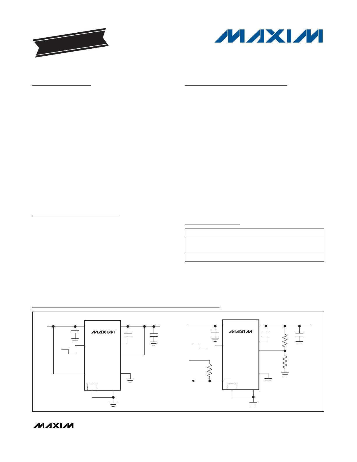
Typical Operating Circuits
+
Denotes a lead-free, RoHS-compliant package.
Note: All devices are in an 8-pin, 2mm x 2mm TDFN package
with an exposed paddle and operate over the -40°C to +125°C
automotive temperature range.
Pin Configurations appear at end of data sheet.
PART FEATURES TOP MARK
MAX8902AATA+
MAX8902BATA+ Adjustable output voltage ABH
Pin-selectable output
voltage
ABG
INPUT
4.7V TO 5.5V
10μF
ON
IN
EN
OFF
SELA
EP
OUT
MAX8902A
BYP
OUTS
SELB
GND
0.01μF
OUTPUT
4.6V
10μF
INPUT
1.7V TO 5.5V
ON
LOGIC
SUPPLY
TO μC
10μF
100kΩ
OUTPUT ADJUSTABLE
0.01μF
0.6V TO 5.3V
10μF
R1
R2
IN
MAX8902B
EN
OFF
R3
POK
EP
OUT
BYP
FB
GS
GND

MAX8902A/MAX8902B
Low-Noise 500mA LDO Regulators
in a 2mm x 2mm TDFN Package
2 _______________________________________________________________________________________
ABSOLUTE MAXIMUM RATINGS
Stresses beyond those listed under “Absolute Maximum Ratings” may cause permanent damage to the device. These are stress ratings only, and functional
operation of the device at these or any other conditions beyond those indicated in the operational sections of the specifications is not implied. Exposure to
absolute maximum rating conditions for extended periods may affect device reliability.
BYP, EN, IN, OUT, SELA, SELB, POK to GND, GS to GND, FB,
OUTS to GND .....................................................-0.3V to +6.0V
Output Short-Circuit Duration.....................................Continuous
Continuous Power Dissipation (T
A
= +70°C)
8-Pin, 2mm x 2mm TDFN
(derate 11.9mW/°C above +70°C).............................953.5mW
Operating Temperature Range .........................-40°C to +125°C
Junction Temperature Range ............................-40°C to +150°C
Storage Temperature Range .............................-65°C to +150°C
Lead Temperature (soldering, 10s) .................................+300°C
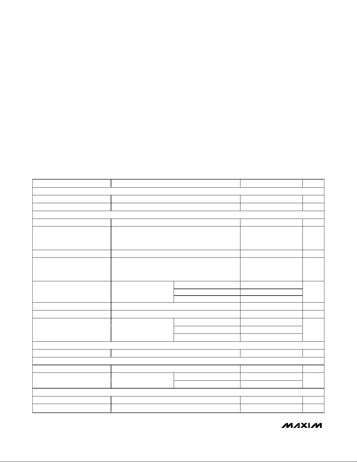
ELECTRICAL CHARACTERISTICS
(VIN= VEN= 5V, OUTS = OUT, circuit of Figure 2 (MAX8902A) and Figure 3 (MAX8902B), TA= -40°C to +125°C, unless otherwise
noted.) (Note 1)
IN
Input Voltage Range 1.7 5.5 V
Input Undervoltage Lockout VIN rising, 100mV typical hysteresis 1.5 1.6 1.7 V
OUT
Output Voltage Range VIN ≥ V
Output Voltage Accuracy
Load Regulation I
Line Regulation
Dropout Voltage
(Note 2)
Current Limit V
Output Noise I
OUTS (MAX8902A only)
OUTS Input Bias Current In regulation 0.5 7.0 µA
FB (MAX8902B only)
FB Threshold Accuracy VIN = 1.7V to 5.5V, I
FB Input Bias Current VFB = 0.6V
BYP
BYP Capacitor Range Regulator remains stable 1 100 nF
BYP Startup Current From BYP to GND during startup 50 µA
PARAMETER CONDITIONS MIN TYP MAX UNITS
+ 0.1V 0.6 5.3 V
OUT
= 1.7V to 5.5V for V
V
IN
= (V
V
IN
I
OUT
OUT
= 1.7V to 5.5V for V
V
IN
= (V
V
IN
I
OUT
I
OUT
OUT
OUT
OUT
+ 0.3V) to 5.5V for V
OUT
= 0.1mA to 500mA
= 0.1mA to 500mA 0.02 %
+ 0.3V) to 5.5V for V
OUT
= 200mA
= 500mA
= 95% of regulation, VIN = V
= 100mA, f = 10Hz to 100kHz, C
= 10mA
OUT
OUT
OUT
≤ 1.4V,
> 1.4V,
OUT
≤ 1.4V,
> 1.4V,
OUT
VIN ≥ 3.6V, TA ≤ +85°C 50 100
VIN ≥ 3.6V, TA ≤ +125°C 120
= 1.7V 150
V
IN
+ 0.5V 600 700 800 mA
OUT
= 0.01µF 16 µV
BYP
f = 5kHz 92
f = 10kHz 85Power-Supply Rejection Ratio I
f = 100kHz 62
= 0.1mA to 500mA 0.591 0.600 0.609 V
TA = +25°C -0.1 0.02 +0.1
T
= -40°C 0.03
A
-1.5 +1.5 %
0.04 %
mV
RMS
dB
µA

MAX8902A/MAX8902B
Low-Noise 500mA LDO Regulators
in a 2mm x 2mm TDFN Package
_______________________________________________________________________________________ 3
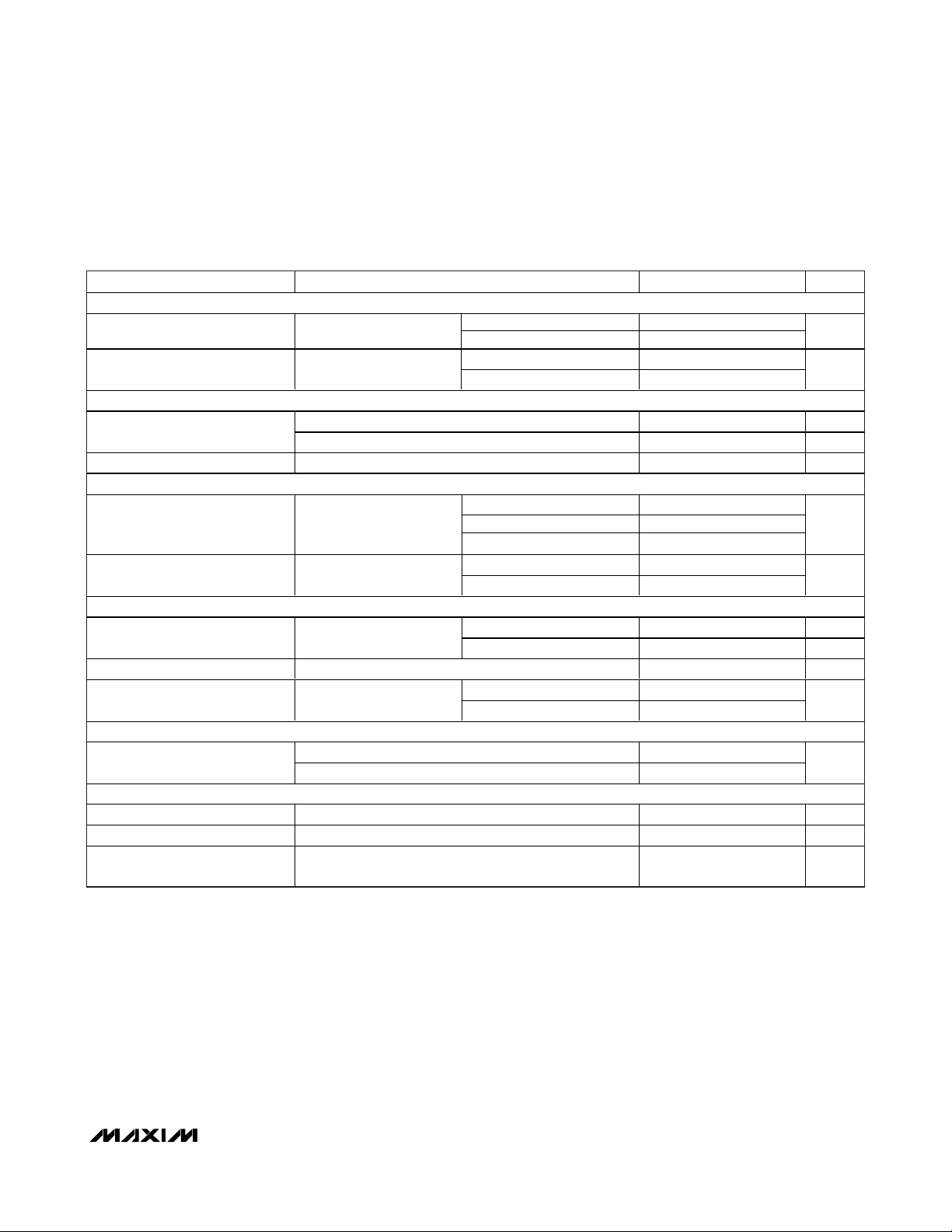
ELECTRICAL CHARACTERISTICS (continued)
(VIN= VEN= 5V, OUTS = OUT, circuit of Figure 2 (MAX8902A) and Figure 3 (MAX8902B), TA= -40°C to +125°C, unless otherwise
noted.) (Note 1)
Note 1: All devices are production tested at TA= +25°C. Specifications over the operating temperature range are guaranteed by
design and characterization.
Note 2: The dropout voltage is defined V
IN
- V
OUT
, when V
OUT
is 5% lower than the value of V
OUT
when VIN= V
OUT
+ 0.5V.
GND
GND Supply Current I
GND Shutdown Current VIN = 5.5V, EN = 0V
SELA/SELB (MAX8902A only)
Select Input Resistance
Select Input Capacitance When open 10 pF
EN
Enable Input Bias Current VEN = 0V to 5.5V
POK (MAX8902B only)
POK Threshold
POK Voltage, Low I
POK Leakage Current POK = 5.5V, VEN = 0V
THERMAL SHUTDOWN
Thermal Shutdown Threshold
OUTPUT TRANSIENT
Load Transient I
Line Transient VIN = 4V to 5V to 4V, t
IN-to-OUT Reverse Voltage
Turnoff Threshold
PARAMETER CONDITIONS MIN TYP MAX UNITS
= 0mA
OUT
When shorted to GND or V
When open 1 MΩ
OUT voltage when POK
switches
= 1mA 10 100 mV
POK
TJ rising 165
T
falling 150
J
= 50mA to 500mA to 50mA, t
OUT
IN falling below OUT 10 mV
TA < +85°C 80 120
T
< +125°C 160
A
TA = +25°C 0.001 +1
= +85°C 0.01
T
A
IN
EN rising 0.8 1.2
EN falling, TA < +85°C 0.4 0.7Enable Input Threshold VIN = 1.7V to 5.5V
EN falling, T
TA = +25°C -1 0.001 +1
= +85°C 0.01
T
A
OUT rising 88 91 94 %
OUT falling 88 %
TA = +25°C -1 0.001 +1
= +85°C 0.01
T
A
RISE
= t
FALL
= 5µs, I
RISE
< +125°C 0.38 0.7
A
= t
= 1µs 25
FALL
= 500mA 3
OUT
µA
µA
500 Ω
µA
µA
°C
mV/
mV/
V
P-P
P-P
 Loading...