

Page 1
General Description
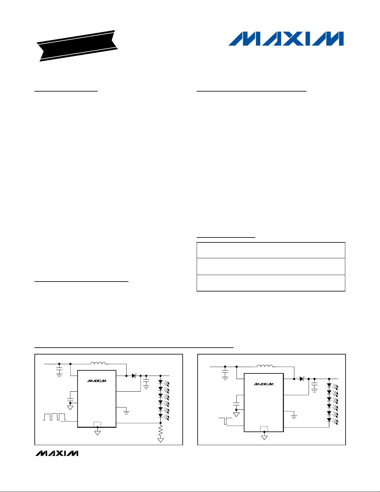
The MAX8901A/MAX8901B step-up converters drive from
two to six series-connected white LEDs (WLEDs) with
constant current to provide uniform WLED intensity for
LCD backlighting in cell phones, PDAs, and other handheld devices. The MAX8901_ operate at a fixed 750kHz
(typ) switching frequency, allowing for tiny external components, and are optimized for the highest possible efficiency over the full 1-cell Li+/Li-Poly battery range.
These converters use a single input (ON) to enable the
IC and to control WLED intensity. The MAX8901A
requires a direct PWM input to regulate WLED intensity
with the WLED current proportional to the PWM duty
cycle. The MAX8901B uses single-wire, serial-pulse
dimming that reduces the WLED intensity in 32 linear
steps. Full-scale WLED current for serial-pulse
dimming is 24.75mA (MAX8901B, 0.75mA/step).
The MAX8901_ features an internal soft-start to eliminate
inrush currents during startup, input overvoltage
protection, WLED overvoltage protection, and a shutdown mode with 0.01µA (typ) shutdown current. No
WLED current is present in shutdown provided the
WLED forward voltage is greater than the input supply
voltage. Additional features include undervoltage lockout (UVLO) and thermal shutdown.
The MAX8901_ are available in tiny 8-pin, 2mm x 2mm
TDFN-EP packages (0.8mm max height).
Applications
Display Backlight (from 2 to 6 WLEDs)
Cellular Phones
PDAs and Smartphones
MP3 and Portable Media Players
Portable Navigation Devices
Digital Cameras
Features
♦ High Efficiency, Up to 91%
♦ 2.6V to 5.5V Input Voltage Range
♦ Fixed-Frequency Operation
♦ Supplies from 2 to 6 WLEDs with 1% LED Current
Accuracy
♦ Flexible Dimming Control
Direct PWM Dimming (MAX8901A)
32-Step, 1-Wire Serial Dimming
(MAX8901B)
♦ Input Undervoltage Lockout
♦ Input Overvoltage Lockout
♦ WLED Overvoltage Protection (25V typ)
♦ 0.01µA (typ) Shutdown Current
♦ No WLED Current in Shutdown
♦ Internal Soft-Start and Thermal Shutdown
MAX8901A/MAX8901B
Highest Efficiency Supply for 2 to 6
Series WLEDs in a 2mm x 2mm TDFN Package
________________________________________________________________
Maxim Integrated Products
1
Ordering Information
MAX8901A
IN
COMP
GND
ON
LX
OVP
PGND
CS
OUTPUT
UP TO 25V
4
1
5
8
2
EP
3
7
6
INPUT
2.6V TO 5.5V
PWM DIMMING
CONTROL
Typical Operating Circuits
19-0865; Rev 0; 8/07
Note: All devices are specified over the -40°C to +85°C operating
temperature range.
+
Denotes a lead-free package.
*
EP = Exposed paddle.
T = Tape and reel.
For pricing, delivery, and ordering information, please contact Maxim Direct at 1-888-629-4642,
or visit Maxim's website at www.maxim-ic.com.
EVALUATION KIT
AVAILABLE
Pin Configuration appears at end of data sheet.
PART PIN-PACKAGE
MAX8901AETA+T
MAX8901BETA+T
8 TDFN-EP*
2mm x 2mm
8 TDFN-EP*
2mm x 2mm
PKG
CODE
T822-1 +ABA
T822-1 +ABB
TOP
MARK
INPUT
2.6V TO 5.5V
OUTPUT
3
IN
MAX8901B
7
COMP
SERIAL-PULSE
DIMMING
CONTROL
6
GND
2
ON
EP
4
LX
1
OVP
5
PGND
8
CS
UP TO 25V
Page 2
MAX8901A/MAX8901B
Highest Efficiency Supply for 2 to 6
Series WLEDs in a 2mm x 2mm TDFN Package
2 _______________________________________________________________________________________
ABSOLUTE MAXIMUM RATINGS
ELECTRICAL CHARACTERISTICS
(VIN= VON= V
OVP
= 3.6V, V
PGND
= V
GND
= 0V, COMP, CS, and LX are unconnected, TA= -40°C to +85°C, unless otherwise noted.
Typical values are at T
A
= +25°C.) (Note 1)
Stresses beyond those listed under “Absolute Maximum Ratings” may cause permanent damage to the device. These are stress ratings only, and functional
operation of the device at these or any other conditions beyond those indicated in the operational sections of the specifications is not implied. Exposure to
absolute maximum rating conditions for extended periods may affect device reliability.
IN to GND .................................................................-0.3V to +7V
CS, COMP, ON to GND ...............................-0.3V to (V
IN
+ 0.3V)
OVP, LX to GND .....................................................-0.3V to +28V
PGND to GND .......................................................-0.3V to +0.3V
LX Current ..................................................................770mA
RMS
Continuous Power Dissipation (multilayer board at +70°C)
8-pin, 2mm x 2mm TDFN
(derate above +70°C by 11.9mW/°C)..........................953mW
Operating Temperature Range ...........................-40°C to +85°C
Junction Temperature......................................................+150°C
Storage Temperature Range .............................-65°C to +150°C
Lead Temperature (soldering, 10s) .................................+300°C
Input Voltage V
Input Undervoltage Lockout
Threshold
Input Overvoltage Lockout
Threshold
Shutdown Input Current I
Quiescent Current I
Output Voltage Range V
OVP Overvoltage Protection
Threshold
OVP Input Current I
CS Regulation Voltage V
ON Shutdown Delay t
ON High Voltage V
ON Low Voltage V
ON Input Current I
Initial ON High Pulse Width t
ON High Pulse Width t
ON Low Pulse Width t
PARAMETER SYMBOL CONDITIONS MIN TYP MAX UNITS
IN
V
IN_UVLO
V
IN_OVLO
SHDN
OUT
V
OV
OV
CS
SHDN
ON_HI
ON_LO
ON
HI_INIT
HI
LO
VIN rising 2.25 2.50
VIN falling 2.20 2.53
VIN rising 6.2 6.3
VIN falling 6.0 6.3
VON = 0V
VCS = 0.55V, no
load (not
Q
switching)
V
= external boost diode voltage drop
DIODE
6 LEDs with 25V OVP option 24 25 26 V
V
= 20V 20 µA
OVP
No dimming 0.475 0.50 0.525 V
Time VON is below low threshold until
shutdown (Figure 1)
2.6V < VIN < 5.5V 1.3 V
2.6V < VIN < 5.5V 0.4 V
ON = IN
First ON high pulse to enable IC
(MAX8901B) (Figure 1)
MAX8901B (Figure 1) 0.5 µs
MAX8901B (Figure 1) 0.5 500.0 µs
2.6 5.5 V
TA = +25°C 0.01 1
= +85°C 0.1
T
A
MAX8901A 70 135
MAX8901B 115 185
V
-
IN
V
DIODE
1.18 1.33 1.50 ms
TA = +25°C 0.01 1
= +85°C 0.1
T
A
40 µs
V
OV
V
V
µA
µA
V
µA
Page 3
MAX8901A/MAX8901B
Highest Efficiency Supply for 2 to 6
Series WLEDs in a 2mm x 2mm TDFN Package
_______________________________________________________________________________________ 3
Note 1: Specifications to -40°C are guaranteed by design and characterization and are not production tested.
ELECTRICAL CHARACTERISTICS (continued)
(VIN= VON= V
OVP
= 3.6V, V
PGND
= V
GND
= 0V, COMP, CS, and LX are unconnected, TA= -40°C to +85°C, unless otherwise noted.
Typical values are at T
A
= +25°C.) (Note 1)
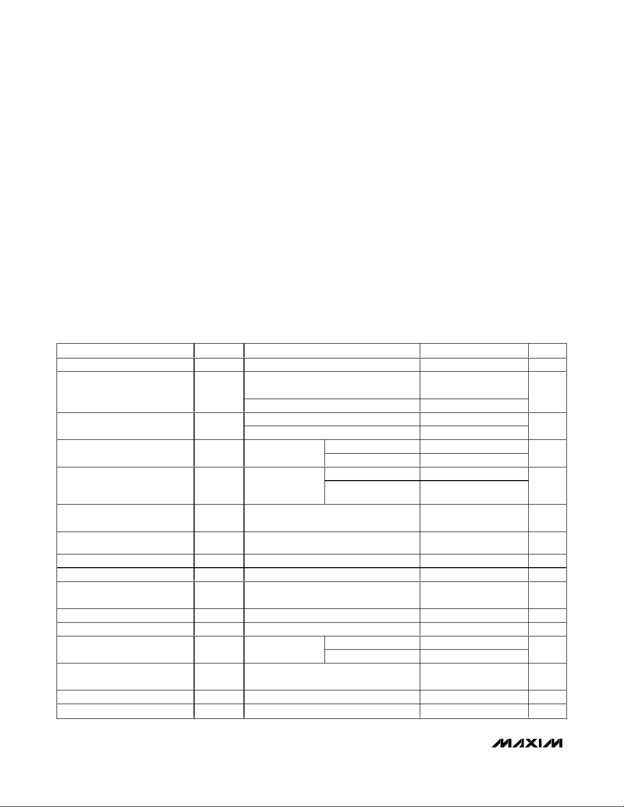
Figure 1. MAX8901B Timing Diagram
Serial Dimming
Full-Scale LED Current Accuracy
PWM Frequency for PWM
Dimming Control
CS to COMP Transconductance 40 60 80 µS
Soft-Start Interval
Thermal Shutdown 160 °C
OSCILLATOR
Operating Frequency f
Maximum Duty Cycle D
n-CHANNEL SWITCH
LX Leakage Current I
n-Channel Switch On-Resistance R
n-Channel Current Limit I
PARAMETER SYMBOL CONDITIONS MIN TYP MAX UNITS
TA = +25°C-1 +1%
T
= -40°C to +85°C-3 +3 %
A
700 750 800 kHz
TA = +25°C 0.1 5
T
= +85°C 0.1
A
0.7 1.4 Ω
0.63 0.70 0.77 A
f
PWM
t
SOFT-
START
SW
MAX
LXLKG
LX
LIM
I
= 24.75mA
LED
(MAX8901B)
MAX8901A 100 kHz
C
= 0.022µF (Figure 1) 10 ms
COMP
VCS = 0.4V 90 92 %
VLX = 27V
µA
STEP
I
LED_
t
HI_INIT
> 40μs
t
SOFT-START
SHUTDOWN
ON
FULL
102 3 4 5 28 29 30 31 32
32/33
31/33
500ns TO 500μs
30/33
29/33
28/33
33
t
6/33
HI
> 500ns
5/33
4/33
3/33
2/33
FULL
1/33
t
LO
32/33
t
SHDN
1.33ms (typ)
SHUTDOWN
Page 4
MAX8901A/MAX8901B
Highest Efficiency Supply for 2 to 6
Series WLEDs in a 2mm x 2mm TDFN Package
4 _______________________________________________________________________________________
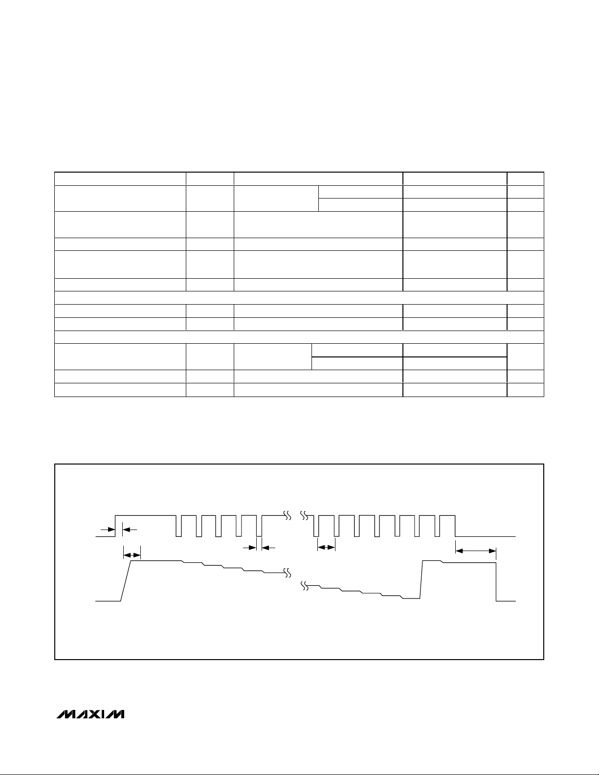
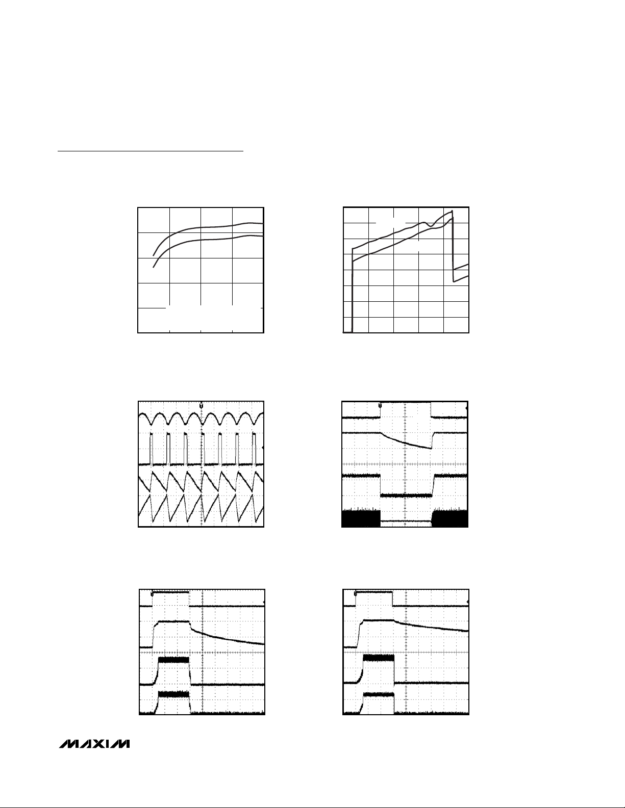
Typical Operating Characteristics
(Circuit of Figure 5, I
LED
= 24.75mA, VIN= VON= 3.6V, C1 = 1µF, C2 = 1µF, TA= +25°C, unless otherwise noted.)
90
85
80
75
70
24356
LED EFFICIENCY vs. INPUT VOLTAGE
MAX8901A/B toc01
INPUT VOLTAGE (V)
EFFICIENCY (%)
4 WLEDs
6 WLEDs
3 WLEDs
INDUCTOR: TOKO 1069AS-220M
DIODE: CENTRAL SEMI CMDSH05-4
90
85
80
75
70
24356
LED EFFICIENCY vs. INPUT VOLTAGE
MAX8901A/B toc02
INPUT VOLTAGE (V)
EFFICIENCY (%)
4 WLEDs
6 WLEDs
3 WLEDs
INDUCTOR: TOKO 1098AS-100M
DIODE: NXP PMEG3005EB
50
55
60
65
70
75
80
85
90
0 5 10 15 20 25
LED EFFICIENCY vs. LED CURRENT
(6 WLEDs)
MAX8901A/B toc03
LED CURRENT (mA)
EFFICIENCY (%)
VIN = 5V
VIN = 5.5V
VIN = 3.6V
VIN = 4.2V
VIN = 3V
INDUCTOR: TOKO 1069AS-220M
DIODE: CENTRAL SEMI CMDSH05-4
50
55
60
65
70
75
80
85
90
0 5 10 15 20 25
LED EFFICIENCY vs. LED CURRENT
(6 WLEDs)
MAX8901A/B toc04
LED CURRENT (mA)
EFFICIENCY (%)
VIN = 5V
VIN = 5.5V
VIN = 3.6V
VIN = 4.2V
VIN = 3V
INDUCTOR: TOKO 1098AS-100M
DIODE: NXP PMEG3005EB
50
55
60
65
70
75
80
85
90
0 5 10 15 20 25
LED EFFICIENCY vs. LED CURRENT
(4 WLEDs)
MAX8901A/B toc05
LED CURRENT (mA)
EFFICIENCY (%)
VIN = 5V
VIN = 5.5V
VIN = 3.6V
VIN = 4.2V
VIN = 3V
INDUCTOR: TOKO 1069AS-220M
DIODE: CENTRAL SEMI CMDSH05-4
50
55
60
65
70
75
80
85
90
0 5 10 15 20 25
LED EFFICIENCY vs. LED CURRENT
(4 WLEDs)
MAX8901A/B toc06
LED CURRENT (mA)
EFFICIENCY (%)
VIN = 5V
VIN = 5.5V
VIN = 3.6V
VIN = 4.2V
VIN = 3V
INDUCTOR: TOKO 1098AS-100M
DIODE: NXP PMEG3005EB
Page 5
MAX8901A/MAX8901B
Highest Efficiency Supply for 2 to 6
Series WLEDs in a 2mm x 2mm TDFN Package
_______________________________________________________________________________________
5
Typical Operating Characteristics (continued)
(Circuit of Figure 5, I
LED
= 24.75mA, VIN= VON= 3.6V, C1 = 1µF, C2 = 1µF, TA= +25°C, unless otherwise noted.)
70
75
85
80
90
95
LED AND BOOST EFFICIENCY
vs. INPUT VOLTAGE
MAX8901A/B toc07
INPUT VOLTAGE (V)
EFFICIENCY (%)
24356
BOOST
LED
6WLEDs,
INDUCTOR: TOKO A915AY-220M,
DIODE: CENTRAL SEMI CMDSH05-4
0
100
200
300
400
500
600
700
800
234567
IN CURRENT (IIN)
vs. SUPPLY VOLTAGE
MAX8901A/B toc08
SUPPLY VOLTAGE (V)
I
IN
(μA)
MAX8901B
MAX8901A
1
μs/div
SWITCHING WAVEFORMS
50mV/div
AC-COUPLED
MAX8901A/B toc9
0mA
10V/div
0V
100mV/div
AC-COUPLED
100mA/div
V
I
V
LX
V
OUT
I
LX
20ms/div
INPUT OVERVOLTAGE
PROTECTION RESPONSE
MAX8901A/B toc10
0V
0mA
10V/div
1V/div
(AC-COUPLED)
0V
20mA/div
20mA/div
V
IN
V
OUT
I
LEDs
V
LX
6.4V
5.4V
10ms/div
STARTUP AND SHUTDOWN
RESPONSE (MAX8901A)
MAX8901A/B toc11
0mA
0mA
10V/div
2V/div
0V
0V
20mA/div
100mA/div
V
ON
V
OUT
I
SUPPLY
I
LEDs
C2 = 0.1μF
10ms/div
STARTUP AND SHUTDOWN
RESPONSE (MAX8901B)
MAX8901A/B toc12
0mA
0mA
10V/div
2V/div
0V
0V
20mA/div
100mA/div
V
ON
V
OUT
I
SUPPLY
I
LEDs
Page 6

MAX8901A/MAX8901B
Highest Efficiency Supply for 2 to 6
Series WLEDs in a 2mm x 2mm TDFN Package
6 _______________________________________________________________________________________
Typical Operating Characteristics (continued)
(Circuit of Figure 5, I
LED
= 24.75mA, VIN= VON= 3.6V, C1 = 1µF, C2 = 1µF, TA= +25°C, unless otherwise noted.)
499.4
499.8
499.6
500.2
500.0
500.8
500.6
500.4
501.0
0105 1520253035
VCS vs. LED CURRENT STEP
(MAX8901B)
MAX8901A/B toc16
LED CURRENT STEP
V
CS
(mV)
I
LED
= 0.75mA
I
LED
= 24.75mA
24.0
24.2
24.6
24.4
24.8
25.0
-40 10-15 35 60
85
MAXIMUM LED CURRENT
vs. TEMPERATURE (MAX8901B)
MAX8901A/B toc17
TEMPERATURE (°C)
I
LED
(mA)
MINIMUM LED CURRENT
vs. TEMPERATURE (MAX8901B)
MAX8901A/B toc18
TEMPERATURE (°C)
I
LED
(μA)
603510-15
735
740
745
750
730
-40 85
4ms/div
PWM DIMMING RESPONSE
(MAX8901A)
MAX8901A/B toc13
0V
0V
0mA
2V/div
0V
20mA/div
20mV/div
V
ON
V
IN
V
CS
V
OUT
I
LEDs
D = 10%
D = 90%
50mV/div
(AC-COUPLED)
500mV/div
f
ON_PWM
= 100kHz, DUTY
CYCLE CHANGE: 90% TO
10%, C2 = 0.1μF
10ms/div
SERIAL PULSE DIMMING
RESPONSE (MAX8901B)
MAX8901A/B toc14
0V
0V
0mA
2V/div
0V
20mA/div
20mV/div
V
ON
V
IN
V
CS
V
OUT
I
LEDs
50mV/div
(AC-COUPLED)
1V/div
0
10
5
20
15
25
30
04020 60 80 100
LED CURRENT vs. PWM
DIMMING (MAX8901A)
MAX8901A/B toc15
PWM DUTY CYCLE (%)
I
LED
(mA)
RCS = 20Ω,
f
PWM
= 100kHz
Page 7

MAX8901A/MAX8901B
Highest Efficiency Supply for 2 to 6
Series WLEDs in a 2mm x 2mm TDFN Package
_______________________________________________________________________________________ 7
Pin Description
PIN NAME FUNCTION
WLED Overvoltage Protection Input. OVP monitors voltage at the WLEDs. Connect OVP to the
1 OVP
2ON
3IN
4 LX Boost Inductor Node. Connect an inductor between IN and LX. LX is high impedance in shutdown.
5 PGND Power Ground. Connect to GND and the exposed paddle (EP) with a short, wide trace.
6 GND Analog Ground. Connect GND to the exposed paddle with a short, wide trace.
7 COMP
8CS
—EP
positive terminal of the output capacitor. If an OVP condition is detected, the MAX8901_ latches off.
Cycle V
Enable and Dimming Control Input. Drive ON high to enable the IC. Drive ON low for greater than
1.33ms (typ) to shutdown the WLED current regulator.
For the MAX8901A: After V
and increases the WLED current to full brightness. Apply a minimum 30kHz (500kHz max) PWM
signal to ON to adjust the WLED brightness from 100% to off, proportional to the duty cycle of the
PWM signal. See the PWM Dimming Control (MAX8901A) section for more details.
For the MAX8901B: After ON is driven high for 40µs (min), the MAX8901B enters soft-start and
increases the WLED current to full brightness. Subsequent pulses on ON cause the MAX8901B
WLED current to decrease in 32 equal steps. See the Serial-Pulse Dimming Control (MAX8901B)
section for more details.
Power Supply Input. Bypass IN to GND with a 1µF ceramic capacitor placed as close as possible to
the IC. If V
switching and no WLED current flows (if the forward voltage of the WLED string is greater than V
When V
initiated and normal operation resumes.
WLED Boost Compensation Node. Connect a 0.022µF ceramic capacitor from COMP to GND.
C
shutdown.
WLED Current Sense Input. For the MAX8901A, connect a current-sense resistor from CS to GND.
Voltage sensed at CS regulates the WLED current. For the MAX8901B, do not connect a sense
resistor from CS to GND. The MAX8901B provides an internal current source from CS to GND to
program the WLED current. The MAX8901B regulates V
regulates V
Exposed Metal Paddle. Connect EP to GND. For good thermal dissipation, the exposed paddle must
be connected to a large ground plane.
or toggle VON to restart the IC.
IN
is above V
IN
exceeds the input overvoltage lockout threshold (6.5V max, VIN rising), the IC stops
IN
falls below the overvoltage lockout hysteresis level (6.0V min, VIN falling), soft-start is
IN
stabilizes the converter and sets the soft-start time. COMP discharges to GND when in
COMP
to 0.5V (typ) for maximum duty cycle only.
CS
and ON is driven high, the MAX8901A enters soft-start
UVLO
to 0.5V (typ) for all I
CS
LED.
The MAX8901A
).
IN
Page 8

MAX8901A/MAX8901B
Highest Efficiency Supply for 2 to 6
Series WLEDs in a 2mm x 2mm TDFN Package
8 _______________________________________________________________________________________
Detailed Description
The high efficiency and tiny size of the MAX8901A/
MAX8901B WLED step-up converters make them ideally
suited for driving LCD backlighting in cell phones, PDAs,
and other portable and handheld devices. The
MAX8901_ drive from 2 to 6 series-connected WLEDs
with constant current for uniform WLED intensity and are
optimized for the highest possible efficiency (up to 91%)
over the full 1-cell Li+/Li-Poly battery range. These tiny
2mm x 2mm devices operate at a constant 750kHz
switching frequency, and use small external components
to achieve minimal input and output ripple while occupying the smallest possible footprint.
These converters use a single input (ON) to enable the IC
and to control WLED intensity. The MAX8901A requires a
direct PWM input to modulate WLED intensity, with WLED
current proportional to the PWM duty cycle. The
MAX8901B uses single-wire, serial-pulse dimming that
reduces the WLED intensity in 32 equal steps. Full-scale
WLED current for serial-pulse dimming is 24.75mA.
Figure 2. MAX8901A Block Diagram
MAX8901A
GND
IC
IN
LX
THERMAL
SHUTDOWN
INTERNAL
750kHz OSC
REF
BOOST
CONTROL
LOGIC
POWER
SHUTDOWN
TIMER
Gm
PGND
OVP
CS
D*0.5V
PWM
COMP
ON
EP
Page 9

MAX8901A/MAX8901B
Highest Efficiency Supply for 2 to 6
Series WLEDs in a 2mm x 2mm TDFN Package
_______________________________________________________________________________________ 9
The MAX8901_ features:
• Internal soft-start that gradually illuminates the
WLEDs to eliminate inrush current during startup.
• Input overvoltage protection (6.5V max) that
prevents IC switching when exceeded.
• WLED overvoltage protection (25V typ) that latches
off the IC.
• Shutdown mode that reduces current to 0.01µA (typ).
No WLED current is present in shutdown or during an
overvoltage condition if the WLED forward voltage is
greater than the input supply voltage. Figures 2 and 3
show the block diagrams for the MAX8901A and
MAX8901B, respectively.
Input Overvoltage Lockout
When VINexceeds 6.2V (min), input overvoltage
lockout (OVLO) is engaged to protect the MAX8901_
from high-input voltage conditions. Once input OVLO
occurs, the MAX8901_ stops switching and no WLED
current flows, provided the forward voltage of the
WLED string is greater than VIN. When VINfalls below
6V (min), the input OVLO condition is cleared, and the
IC is enabled and enters soft-start.
WLED Overvoltage Protection
WLED overvoltage protection (OVP) occurs when the
WLED output voltage rises above the WLED OVP
threshold. The WLED OVP protection circuitry latches
off the IC and the IC enters shutdown when the WLED
OVP threshold is exceeded. After OVP is engaged,
cycle VINor toggle ON to reenable the IC and enter
soft-start.
Figure 3. MAX8901B Block Diagram
MAX8901B
IC
POWER
GND
IN
LX
THERMAL
SHUTDOWN
INTERNAL
750kHz OSC
REF
BOOST
CONTROL
LOGIC
SHUTDOWN
TIMER
Gm
PGND
OVP
CS
0.5V
EP
PULSE
DIMMING
COMP
ON
Page 10

MAX8901A/MAX8901B
Highest Efficiency Supply for 2 to 6
Series WLEDs in a 2mm x 2mm TDFN Package
10 ______________________________________________________________________________________
Startup and Soft-Start
The MAX8901_ use a single input (ON) to enable the IC
and to control WLED intensity. After ON is driven high,
the MAX8901_ enter soft-start and gradually increase
the WLED current to full brightness.
When the MAX8901_ is first turned on, C
COMP
is
charged to 1.25V with a 60µA current source. When
V
COMP
rises above 1.25V, C
COMP
is charged with a
4µA current source, and the internal MOSFET begins
switching at a reduced duty cycle. When V
COMP
rises
above 2.25V, the duty cycle is at its maximum. The
V
COMP
where the IC exits soft-start depends on the
final duty cycle required by the load. Typical shutdown
timing characteristics are shown in the
Typical
Operating Characteristics
section.
A PWM signal (MAX8901A) or serial pulses (MAX8901B)
are applied to dim the WLEDs. See the
PWM Dimming
Control (MAX8901A)
and
Serial-Pulse Dimming Control
(MAX8901B)
sections for more details.
Shutdown
The MAX8901_ enter shutdown when VONis held low
for more than 1.33ms (typ), or when an output overvoltage condition is engaged. In shutdown, the supply current is reduced to 0.01µA (typ) by powering down the
entire IC except for the ON voltage-detection circuitry.
C
COMP
is discharged to GND during shutdown,
allowing the device to reinitiate soft-start when it is
re-enabled. Although the internal n-channel MOSFET
does not switch in shutdown, there is still a DC current
path between the input and the WLEDs through the
inductor and Schottky diode. In shutdown, the minimum
forward voltage of the WLED string must exceed the
maximum input voltage to ensure that the WLEDs
remain off. Typically, with two or more WLEDs, the forward voltage is large enough to keep leakage current
low, less than 1µA (typ). Shutdown timing characteristics are shown in the
Typical Operating Characteristics
.
Thermal Shutdown
The MAX8901 includes a thermal shutdown feature that
protects the IC by turning it off when the die temperature
reaches +160°C (typ). After thermal shutdown occurs,
the MAX8901_ must be restarted by toggling the ON pin
low, then high, or by cycling the input voltage.
PWM Dimming Control (MAX8901A)
After VINis above UVLO, apply a PWM signal to ON for
a WLED current that is proportional to the PWM signal’s
duty cycle (0% duty cycle corresponds to zero LED
current and 100% duty cycle corresponds to full LED
current). Restrict PWM frequency to between 30kHz to
500kHz for a maximum I
LED
current accuracy. If dimming control is not required, ON works as a simple on/off
control. Drive ON high to enable the IC, or drive ON low
for shutdown. A resistor connected from CS to GND programs maximum I
LED
. See the
Current-Sense Resistor
(MAX8901A Only)
section for more details.
Serial-Pulse Dimming Control (MAX8901B)
After the MAX8901B is enabled by driving ON high for
the minimum initial ON high pulse width (40µs, min),
soft-start is engaged and brings WLED current to maximum brightness. After soft-start is completed, dim the
MAX8901B by pulsing ON low (500ns to 500µs pulse
width). Each pulse reduces the WLED current by
0.75mA. The maximum WLED current is 24.75mA for
the MAX8901B (0.75mA/step). The overall dimming
range for serial-pulse dimming control is from maximum
WLED current down to 1/33 of maximum WLED current.
The WLEDs are turned off by holding ON low for at
least 1.33ms (typ). See Figure 1 for the serial-pulse
dimming control timing diagram.
Applications Information
Inductor Selection
Recommended inductor values range from 10µH to
47µH. A 22µH inductor optimizes the efficiency for most
applications while maintaining low input voltage ripple.
With input voltages near 5V, a larger value of
inductance may be more efficient. To prevent core
saturation, ensure that the inductor saturation current
rating exceeds the peak inductor current for the
application. Calculate the peak inductor current with
the following formula:
where I
LED(MAX)
is in mA and L is in µH.
I
PEAK
V
OUT(MAX)
=
×+I
LED MAX()
V
x
900 2
IN(MIN)
V
IN(MIN) x .2
1
x L
Page 11

MAX8901A/MAX8901B
Highest Efficiency Supply for 2 to 6
Series WLEDs in a 2mm x 2mm TDFN Package
______________________________________________________________________________________ 11
Schottky Diode Selection
The high switching frequency of the MAX8901_
demands a high-speed rectification diode for optimum
efficiency. A Schottky diode is recommended due to its
fast recovery time and low forward voltage drop.
Ensure that the diode’s average and peak current
rating exceeds the average output current and peak
inductor current. In addition, the diode’s reverse
breakdown voltage must exceed V
OUT
. The RMS diode
current can be approximated from the following
equation:
Capacitor Selection
Ceramic capacitors with X5R, X7R, or better dielectric
are recommended for stable operation over the entire
operating temperature range. The exact values of input
(C1) and output (C2) capacitors are not critical (see
Figures 4 and 5). The typical value for the input
capacitor is 1µF, and the typical value for the output
capacitor is 0.1µF (MAX8901A) or 1µF (MAX8901B).
Higher value capacitors can reduce input and output
ripple, but at the expense of size and higher cost. The
compensation capacitor (C3) stabilizes the converter
and controls soft-start. The compensation capacitor is
typically chosen to be 0.022µF for most applications.
Current-Sense Resistor (MAX8901A Only)
The MAX8901A uses a sense resistor (RCS) connected
from CS to GND to program the maximum WLED current for 100% PWM duty cycle. The MAX8901A regulates V
CS
to 0.5V (typ) for 100% duty cycle. Calculate
RCS(in ohms) using the following equation:
where I
LED(MAX)
is the maximum WLED current in
milliamps. Maximum WLED current is programmed to
25mA using a 20Ω resistor.
PCB Layout
Due to fast switching waveforms and high-current
paths, careful attention is required when the PCB layout
is designed. Minimize trace lengths between the IC and
the inductor, the diode, the input capacitor, and the
output capacitor. For the MAX8901A, minimize the
trace length between the IC and R
CS
. Keep traces
short, direct, and wide. Keep noisy traces, such as the
LX node trace, away from CS. The input bypass
capacitor (CIN) should be placed as close as possible
to the IC. The ground connections of CINand C
OUT
should be as close together as possible. PGND and
GND should be connected together at the input
capacitor ground terminal. Refer to the MAX8901 EV Kit
for an example layout.
I
DIODE RMS()
=× II
LED PEAK
=
I
LED(MAX)
500
R
CS
Page 12

MAX8901A/MAX8901B
Highest Efficiency Supply for 2 to 6
Series WLEDs in a 2mm x 2mm TDFN Package
12 ______________________________________________________________________________________
Figure 4. MAX8901A Application Circuit
Figure 5. MAX8901B Application Circuit
INPUT
2.6V TO 5.5V
C1
1μF
0.022μF
PWM DIMMING
CONTROL
INPUT
2.6V TO 5.5V
C1
1μF
0Ω
3
IN
COMP
GND
ON
IN
COMP
MAX8901A
MAX8901B
7
C3
6
2
3
7
R1
L1
22μH
EP
L1
22μH
OVP
PGND
OVP
C2
0.1μF
C2
1μF
OUTPUT
UP TO 25V
R1 (R
20Ω
OUTPUT
UP TO 25V
D2–D7
)
CS
4
LX
1
5
8
CS
4
LX
1
D1
D1
SERIAL-PULSE
DIMMING
CONTROL
0.022μF
C3
6
GND
2
ON
EP
PGND
5
8
CS
Page 13
MAX8901A/MAX8901B
Highest Efficiency Supply for 2 to 6
Series WLEDs in a 2mm x 2mm TDFN Package
______________________________________________________________________________________ 13
Pin Configuration
Chip Information
PROCESS: BiCMOS
TOP VIEW
*EXPOSED PAD
CS PGND
COMP
GND
865
7
MAX8901
+
1
2
OVP IN LXON
TDFN-EP
(2mm × 2mm)
*EP
34
Page 14

MAX8901A/MAX8901B
Highest Efficiency Supply for 2 to 6
Series WLEDs in a 2mm x 2mm TDFN Package
14 ______________________________________________________________________________________
Package Information
(The package drawing(s) in this data sheet may not reflect the most current specifications. For the latest package outline information
go to www.maxim-ic.com/packages
.)
8L TDFN EXPOSED PADS.EPS
PACKAGE OUTLINE
6 & 8L TDFN EXPOSED PAD, 2x2x0.80mm
21-0168
1
D
2
Page 15

MAX8901A/MAX8901B
Highest Efficiency Supply for 2 to 6
Series WLEDs in a 2mm x 2mm TDFN Package
Maxim cannot assume responsibility for use of any circuitry other than circuitry entirely embodied in a Maxim product. No circuit patent licenses are
implied. Maxim reserves the right to change the circuitry and specifications without notice at any time.
Maxim Integrated Products, 120 San Gabriel Drive, Sunnyvale, CA 94086 408-737-7600 ____________________
15
© 2007 Maxim Integrated Products is a registered trademark of Maxim Integrated Products, Inc.
Package Information (continued)
(The package drawing(s) in this data sheet may not reflect the most current specifications. For the latest package outline information
go to www.maxim-ic.com/packages
.)
MIN.
0.70
1.90
0.00
0.20
0.25 MIN.
0.20 REF.
MAX.
0.80
2.101.90
2.10
0.05
0.40
N
0.90±0.10
6
E2D2
1.60±0.10 1.30 REF
1.30±0.10 1.50 REF0.25±0.050.50 TYP. 0.70±0.108T822-1
1.20±0.10 1.50 REF0.25±0.050.50 TYP. 0.80±0.108T822-2 0.125
e
0.65 TYP.
b
0.30±0.05
r
0.150
0.125
[(N/2)-1] x e
COMMON DIMENSIONS
SYMBOL
A
D
E
A1
L
k
A2
PACKAGE VARIATIONS
PKG. CODE
T622-1
PACKAGE OUTLINE
6 & 8L TDFN EXPOSED PAD, 2x2x0.80mm
21-0168
2
D
2
 Loading...