MAXIM MAX889 Technical data

General Description
The MAX889 inverting charge pump delivers a regulated
negative output voltage at loads of up to 200mA. The
device operates with inputs from 2.7V to 5.5V to produce
an adjustable, regulated output from -2.5V to -VIN.
The MAX889 is available with an operating frequency of
2MHz (T version), 1MHz (S version), or 0.5MHz (R version). The higher switching frequency devices allow the
use of smaller capacitors for space-limited applications. The lower frequency devices have lower quiescent current.
The MAX889 also features a 0.1µA logic-controlled
shutdown mode and is available in an 8-pin SO package. An evaluation kit, MAX889SEVKIT, is available.
________________________Applications
TFT Panels
Hard Disk Drives
Camcorders
Digital Cameras
Measurement Instruments
Battery-Powered Applications
Features
♦ 200mA Output Current
♦ Up to 2MHz Switching Frequency
♦ Small Capacitors (1µF)
♦ +2.7V to +5.5V Input Voltage Range
♦ Adjustable Regulated Negative Output
(-2.5V to -V
IN
)
♦ 0.1µA Logic-Controlled Shutdown
♦ Low 0.05Ω Output Resistance (in regulation)
♦ Soft-Start and Foldback Current Limited
♦ Short-Circuit and Thermal Shutdown Protected
♦ 8-Pin SO Package
MAX889
High-Frequency, Regulated,
200mA, Inverting Charge Pump
________________________________________________________________ Maxim Integrated Products 1
Pin Configuration
MAX889
IN
INPUT +2.7V TO +5.5V
REGULATED
NEGATIVE
OUTPUT
(UP TO -1 × V
IN
,
UP TO 200mA)
FB
OUT
GNDAGND
CAP+
ON
OFF
SHDN
CAP-
Typical Operating Circuit
19-1774; Rev 0; 7/00
For free samples and the latest literature, visit www.maxim-ic.com or phone 1-800-998-8800.
For small orders, phone 1-800-835-8769.
Ordering Information
PART
TEMP.
RANGE
PIN-
SWITCHING
FREQUENCY
8 SO 2MHz
8 SO 1MHz
8 SO 0.5MHz
EVALUATION KIT
AVAILABLE
查询MAX889供应商
PACKAGE
MAX889TESA -40°C to +85°C
MAX889SESA -40°C to +85°C
MAX889RESA -40°C to +85°C
TOP VIEW
IN
1
2
GND
3
4
87AGND
MAX889
SO
FBCAP+
SHDN
6
OUTCAP-
5

MAX889
High-Frequency, Regulated,
200mA, Inverting Charge Pump
2 _______________________________________________________________________________________
ABSOLUTE MAXIMUM RATINGS
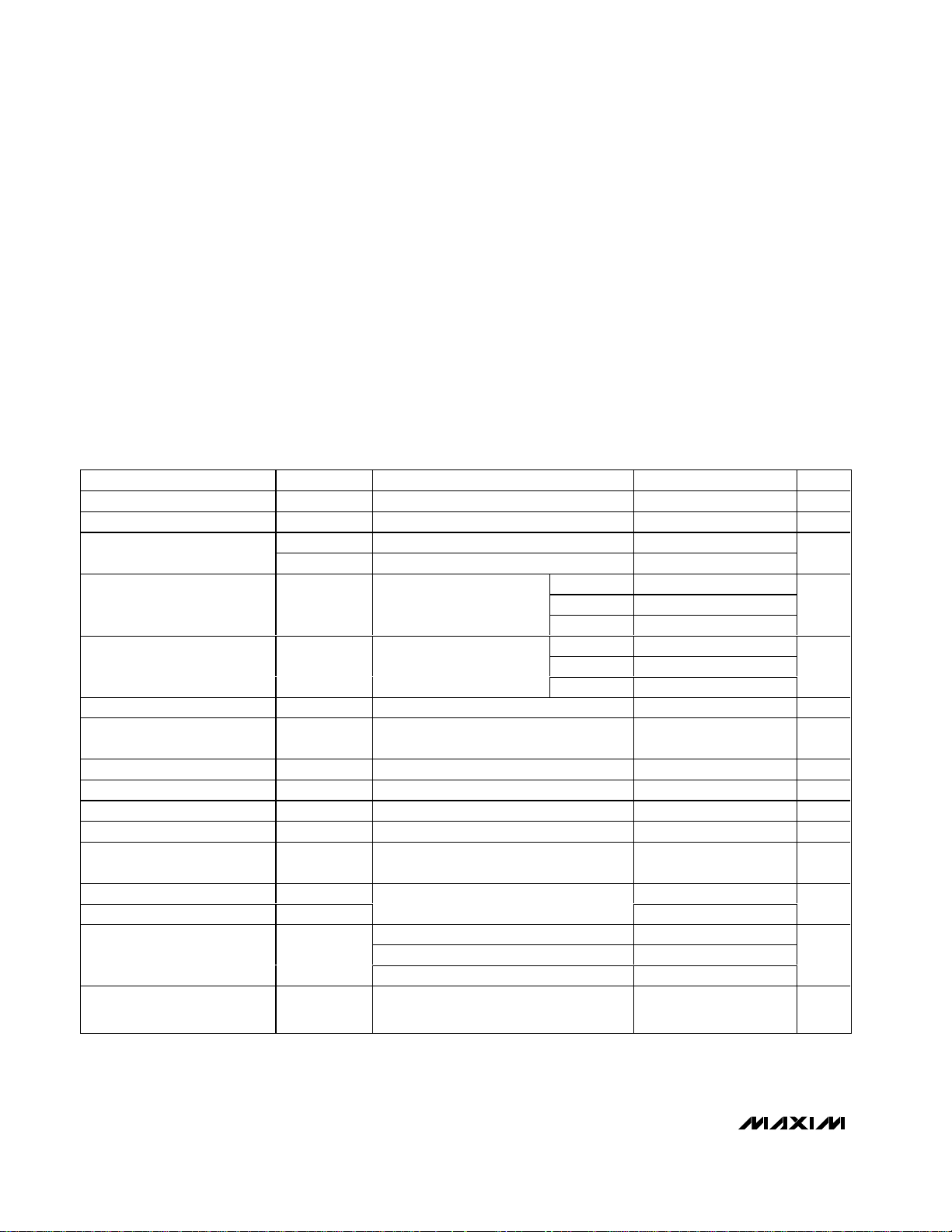
ELECTRICAL CHARACTERISTICS
(VIN= V
SHDN
= +5V, capacitors from Table 1, TA= 0°C to +85°C, unless otherwise noted. Typical values are at TA= +25°C.)
Stresses beyond those listed under “Absolute Maximum Ratings” may cause permanent damage to the device. These are stress ratings only, and functional
operation of the device at these or any other conditions beyond those indicated in the operational sections of the specifications is not implied. Exposure to
absolute maximum rating conditions for extended periods may affect device reliability.
IN to GND .................................................................-0.3V to +6V
FB, SHDN, CAP+ to GND............................-0.3V to (V
IN
+ 0.3V)
AGND to GND .......................................................-0.3V to +0.3V
OUT to GND .............................................................-6V to +0.3V
CAP- to GND ............................................(V
OUT
- 0.3V) to +0.3V
Continuous Output Current ...............................................250mA
Output Short-Circuit Duration ........................................Indefinite
Continuous Power Dissipation (T
A
= +70°C)
8-Pin SO (derate 5.88mW/°C above +70°C)...............471mW
Operating Temperature Range...........................-40°C to +85°C
Junction Temperature......................................................+150°C
Storage Temperature Range .............................-65°C to +150°C
Lead Temperature (soldering, 10s) ................................+300°C
PARAMETER
CONDITIONS
Supply Voltage Range V
IN
R
LOAD
= 100Ω 2.7
V
Output Voltage Range V
OUT
R
LOAD
= 100Ω
V
VIN = 5V, V
OUT
= -3.3V
Maximum Output Current
VIN = 3.3V, V
OUT
= -2.5V
mA
MAX889R 6 12
MAX889S 12 24
Quiescent Supply
Current (Free-Run Mode)
)
No load, VFB = V
IN
MAX889T 24 48
mA
MAX889R 3.3 7
MAX889S 5.5 12
Quiescent Supply
Current (Regulated Mode)
)
-3.3V
MAX889T 11 22
mA
Shutdown Supply Current I
SHDN
V
SHDN
= 0 0.1 50 µA
Open-Loop Output
Resistance (Free-Run Mode)
R
O
VFB = V
IN
2.0
Ω
Output Resistance
R
O(REG1)
V
OUT
regulated to -3.3V
Ω
SHDN, FB Input Bias Current ±1 µA
FB Input Offset Voltage I
LOAD
= 0 ±3
mV
Load Regulation I
OUT
= 0 to 200mA 10 mV
IN Undervoltage Lockout
Threshold
V
IN
rising (30mV hysteresis) 2.3
V
SHDN Logic High V
IH
SHDN Logic Low V
IL
VIN = +2.7V to +5.5V
V
MAX889R
0.5
0.62
MAX889S
1
Switching Frequency f
OSC
MAX889T 1.5 2
Thermal Shutdown Threshold
Junction temperature rising
(15°C hysteresis)
160 °C
SYMBOL
MIN TYP MAX UNITS
-2.5 -V
I
OUT(MAX)1
I
OUT(MAX)2
I
Q(FREE-RUN
200
145
5.5
IN
I
Q(REGULATED
No load, V
regulated to
OUT
0.7 x V
0.375
0.75
0.05
IN
0.3 x V
4.5
±35
2.6
1.25
2.5
IN
MHz

MAX889
High-Frequency, Regulated,
200mA, Inverting Charge Pump
_______________________________________________________________________________________ 3
Note 1: Specifications to -40°C are guaranteed by design, not production tested.
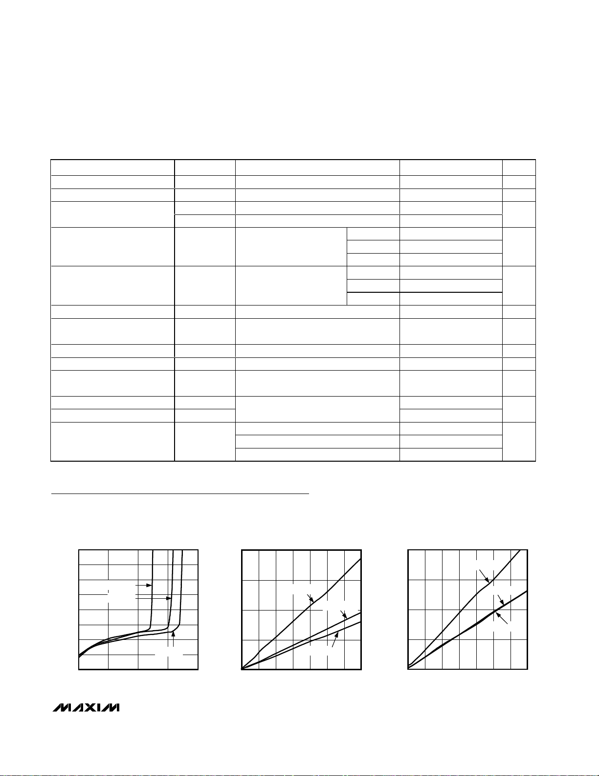
ELECTRICAL CHARACTERISTICS
(VIN= V
SHDN
= +5V, capacitors from Table 1, TA= -40°C to +85°C, unless otherwise noted.) (Note 1)
PARAMETER
CONDITIONS
UNITS
Supply Voltage Range V
IN
R
LOAD
= 100Ω 2.7
V
Output Voltage Range V
OUT
R
LOAD
= 100Ω
V
VIN = 5V, V
OUT
= -3.3V
Maximum Output Current
VIN = 3.3V, V
OUT
= -2.5V
mA
MAX889R 12
MAX889S 24
Quiescent Supply
Current (Free-Run Mode)
)
No load, VFB = V
IN
MAX889T 48
mA
MAX889R 7
MAX889S 12
Quiescent Supply
Current (Regulated Mode)
)
-3.3V
MAX889T 22
mA
Shutdown Supply Current I
SHDN
V
SHDN
= 0 50 µA
Open-Loop Output
Resistance (Free-Run Mode)
R
O
VFB = V
IN
Ω
SHDN FB Input Bias Current ±1 µA
FB Input Offset Voltage I
LOAD
= 0
mV
IN Undervoltage Lockout
Threshold
V
IN
rising (30mV hysteresis) 2.3
V
SHDN Logic High V
IH
SHDN Logic Low V
IL
VIN = +2.7V to +5.5V
V
MAX889R
0.62
MAX889S
Switching Frequency f
OSC
MAX889T 1.5
MHz
Typical Operating Characteristics
(Circuit of Figure 1, VIN= V
SHDN
= +5V, capacitors from Table 1, TA= +25°C, unless otherwise noted.)
OUTPUT VOLTAGE
vs. LOAD CURRENT
MAX889 toc01
OUTPUT LOAD CURRENT (mA)
OUTPUT VOLTAGE (V)
-3.33
-3.32
-3.31
-3.30
-3.29
-3.28
-3.27
-3.26
-3.25
0 200 400 600 800
MAX889T
MAX889S
MAX889R
0
10
20
30
40
MAX889R
OUTPUT RIPPLE
vs. LOAD CURRENT vs. C
OUT
MAX889 toc02
LOAD CURRENT (mA)
OUTPUT RIPPLE (mV)
0 150 20050 100 250 300 350
C
OUT
= 22µF
C
OUT
= 47µF
C
OUT
= 10µF
0
10
20
30
40
MAX889S
OUTPUT RIPPLE
vs. LOAD CURRENT vs. C
OUT
MAX889 toc03
LOAD CURRENT (mA)
OUTPUT RIPPLE (mV)
0 150 20050 100 250 300 350
C
OUT
= 4.7µF
C
OUT
= 22µF
C
OUT
= 10µF
SYMBOL
I
OUT(MAX)1
I
OUT(MAX)2
I
Q(FREE-RUN
I
Q(REGULATED
No load, V
regulated to
OUT
MIN MAX
-2.5 -V
200
145
0.7 x V
IN
0.3 x V
0.375
0.75 1.25
5.5
IN
4.5
±35
2.6
IN
2.5
 Loading...