

For free samples & the latest literature: http://www.maxim-ic.com, or phone 1-800-998-8800.
For small orders, phone 1-800-835-8769.
General Description
The MAX886/MAX888 power-management ICs are complete power systems for wireless and satellite handsets.
The devices operate from 3 to 6-cell NiCd/NiMH batteries or from 1 or 2-cell Li-Ion batteries. They incorporate a
high-efficiency, step-down DC-DC converter, a regulated
5V charge pump, and four linear regulators. The regulators supply power to the SIM, LCD, BB, DSP, and RF
sections of a cellular telephone handset. The step-down
converter and linear regulator outputs are adjustable by
internal 4-bit DACs, programmable through the I2C™compatible serial interface. A pushbutton on/off scheme
activates a 5µA low-power shutdown mode. The devices
also feature a low-battery detector output and an internal
start-up timer.
The MAX886/MAX888 differ in output voltage range and
power-on reset voltage. The MAX886 has a higher preset
voltage range and is intended for 2-cell Li-Ion or 5/6-cell
NiCd/NiMH batteries. The MAX888 has a lower preset
voltage range and is intended for 1-cell Li-Ion or 3/4-cell
NiCd/NiMH batteries. Both devices are available in a
space-saving, 32-pin TQFP package.
Applications
Satellite Phones Private Mobile Radio (PMR)
Wireless Handsets GSM Cellular/PCS Telephones
Features
♦ 90% Efficient, 500mA Step-Down Converter
♦ Two 100mA DAC-Controlled LDOs
One 200mA DAC-Controlled LDO
One 20mA DAC-Controlled LDO
♦ 3 to 6-Cell NiCd or NiMH Operation
1 or 2-Cell Li-Ion Operation
♦ +2.7V to +12V Input Voltage Range
♦ 250µA Standby (PFM) Quiescent Current
♦ 5µA Shutdown Current
♦ I2C-Compatible Serial Interface
♦ Selectable 375kHz, 535kHz, 670kHz, 925kHz
(or Synchronizable) Switching Frequency
♦ Power-On Reset and Start-Up Timer
♦ Thermal Overload Protection
♦ Pushbutton On/Off Control
♦ Space-Saving 32-Pin TQFP Package (7mm x 7mm)
MAX886/MAX888
Wireless and Satellite Handset
Power-Management ICs
________________________________________________________________
Maxim Integrated Products
1
BATT
LBO
SCL
SDA
LBI
IN
2.7V TO 12V
I
2
C-COMPATIBLE
SERIAL INTERFACE
LOW-BATTERY
DETECT
ON/OFF CONTROL
(OPTIONAL)
LX
MAIN POWER (UP TO 500mA)
PGND
OUT0
Tx SECTION POWER (UP TO 100mA)
DSP POWER (UP TO 200mA)
3V/5V SIM CARD POWER (UP TO 20mA)
LCD/VCO/TXCO POWER (UP TO 100mA)
POWER-ON RESET
Rx SECTION POWER (UP TO 100mA)
OUT1
MAX886
MAX888
OUT2
RESET
OUT3
OUT4
OUT5
ONSTAT
GND
OFF
SYNC
C+
C-
ON
ON STATUS
19-1438; Rev 0; 3/99
PART
MAX886ECJ*
MAX888ECJ
-40°C to +85°C
-40°C to +85°C
TEMP. RANGE PIN-PACKAGE
32 TQFP
32 TQFP
EVALUATION KIT MANUAL
FOLLOWS DATA SHEET
*
Future product—contact factory for availability.
Typical Operating Circuit
Ordering Information
Pin Configuration appears at end of data sheet.
I
2
C is a trademark of Philips Corp.

MAX886/MAX888
Wireless and Satellite Handset
Power-Management ICs
2 _______________________________________________________________________________________
ABSOLUTE MAXIMUM RATINGS
ELECTRICAL CHARACTERISTICS
(V
BATT
= V
IN0
= V
IN1
= +5.5V, GND = PGND = DGND, V
OFF
= V
SYNC
= 2.8V, V
IN2
= V
IN3
= V
IN4
= V
IN5
= +3.8V, V
OUT4
= +5.5V,
T
A
= -40°C to +85°C, unless otherwise noted. Typical values are at TA= +25°C.) (Note 1)
Stresses beyond those listed under “Absolute Maximum Ratings” may cause permanent damage to the device. These are stress ratings only, and functional
operation of the device at these or any other conditions beyond those indicated in the operational sections of the specifications is not implied. Exposure to
absolute maximum rating conditions for extended periods may affect device reliability.
BATT, IN0, IN1 to GND...........................................-0.3V to +13V
CVH to IN0................................................................-6V to +0.3V
PGND, DGND to GND...........................................-0.3V to +0.3V
ONSTAT to GND.....................................-0.3V to (V
OUT2
+ 0.3V)
LX to PGND.............................................-0.3V to (V
OUT0
+ 0.3V)
OUT1 to GND.............................................-0.3V to (V
IN1
+ 0.3V)
OUT2 to GND.............................................-0.3V to (V
IN2
+ 0.3V)
OUT3 to GND.............................................-0.3V to (V
IN3
+ 0.3V)
OUT5 to GND.............................................-0.3V to (V
IN5
+ 0.3V)
SYNC, RESET, SCL, SDA, CVL, LBI, LBHYS, OUT0
REF, LBO, C+, C-, OUT4, IN2, IN3, IN4, IN5,
ON, OFF to GND ...................................................-0.3V to +6V
Continuous Power Dissipation (T
A
= +70°C)
TQFP (derate 11.1mW/°C above +70°C)......................889mW
Operating Temperature Range. ......................... -40°C to +85°C
Junction Temperature......................................................+150°C
Storage Temperature Range.............................-65°C to +150°C
Lead Temperature (soldering, 10sec).............................+300°C
V
OUT0
= 3.75V (MAX886),
V
OUT0
= 2.027V (MAX888)
MAX888
MAX886
I
OUT0
= 0
2.7V < V
OUT0
< 3.75V
f
OSC
= 375kHz
1µA < I
REF
< 100µA
I
REF
= 0
SYNC = GND
V
BATT
falling
V
BATT
rising
CONDITIONS
% of
V
OUT0
Output Ready Threshold -7.5 -5 -3
V
1.527 3.027
V
OUT0
Nominal Output Adjustment
Range
2.625 3.750
%-3 3Output Accuracy
V2.7 12V
IN0
Input Voltage Range
mV0.2 5Reference Supply Rejection
mV515Reference Load Regulation
V
1.225 1.275
V
REF
Reference Output Voltage
1.23 1.25 1.27
V2.7 5.5
V
IN2
, V
IN3
,
V
IN4
, V
IN5
IN2, IN3, IN4, IN5 Operating
Voltage Range
V2.7 12
V
BATT
, V
IN0
,
V
IN1
BATT, IN0, IN1 Operating Voltage
Range
510
2
µA250 600I
BATTPFM
Supply Current, PFM Mode
V2.35 2.45V
UVLOF
V2.55 2.65V
UVLOR
Undervoltage Lockout
UNITSMIN TYP MAXSYMBOLPARAMETER
OFF = GND
µA
15
I
STNBY
Supply Current, Shutdown Mode
TA= 0°C to +85°C
TA= -40°C to +85°C
TA= 0°C to +85°C
TA= -40°C to +85°C
f
OSC
= 535kHz 3
f
OSC
= 670kHz
f
OSC
= 925kHz
mA
5.5 12
I
BATTPWM
Supply Current, PWM Mode
4
REFERENCE
DC-DC BUCK REGULATOR 0 (IN0, OUT0)
MAX886/MAX888
Wireless and Satellite Handset
Power-Management ICs
_______________________________________________________________________________________ 3
ELECTRICAL CHARACTERISTICS (continued)
(V
BATT
= V
IN0
= V
IN1
= +5.5V, GND = PGND = DGND, V
OFF
= V
SYNC
= 2.8V, V
IN2
= V
IN3
= V
IN4
= V
IN5
= +3.8V, V
OUT4
= +5.5V,
T
A
= -40°C to +85°C, unless otherwise noted. Typical values are at TA= +25°C.) (Note 1)
I
OUT1
= 0.1mA to 100mA
Table 4
I
OUT0
V
IN0
= 3.8V
CONDITIONS
%-3 3Output Accuracy
V2.7 12V
IN1
Input Voltage Range
%
-23 23
f
OSC
Oscillator Frequency Accuracy
-20 20
A0.6 0.9 1.2I
LIMIT
Internal Switch Current Limit
mA63 98 180PFM to PWM Threshold
Ω0.4 1R
ON
Internal Switch On-Resistance
UNITSMIN TYP MAXSYMBOLPARAMETER
V
OUT2
= 3.3V (MAX886),
V
OUT2
= 1.527V (MAX888)
MAX888
MAX886
I
OUT2
= 0.1mA to 200mA
3V < V
IN1
< 12V, 0h code
I
OUT1
= 0.1mA to 100mA
I
OUT1
= 100mA
I
OUT1
= 1mA
MAX888
MAX886
V
1.527 3.027
V
OUT2
Nominal Output Adjustment
Range
2.175 3.30
%-3 3Output Accuracy
V2.7 5.5V
IN2
Input Voltage Range
mA100 250Current Limit
%/V-0.1 0 0.1Line Regulation
%/mA-0.01 0.01Output Load Regulation
mV
90 200
Dropout Voltage
1
V
1.25 3.5
V
OUT1
Nominal Output Adjustment
Range
2.70 4.95
2.7V < V
IN2
< 3.8V, 0h code
I
OUT2
= 0.1mA to 200mA
I
OUT2
= 200mA
I
OUT2
= 1mA
mA200 500Current Limit
%/V-0.3 0.3Line Regulation
%/mA-0.005 0.002Output Load Regulation
90 200
Dropout Voltage mV
1
% of
V
OUT2
-7.5 -5 -3V
RDY2
Output Ready Threshold
I
OUT3
= 0.1mA to 20mA %-3 3Output Accuracy
V2.7 5.5V
IN3
Input Voltage Range
kHz
0.8 ·
f
OSC
1.2 ·
f
OSC
f
OSC
SYNC Range
TA= 0°C to +85°C
TA= -40°C to +85°C
VLX= 12V µA0.1 10LX Leakage Current
VLX= 12V %100Maximum Duty Cycle
3V < V
IN0
< 12V %-0.3 0 0.3Line Regulation
I
OUT0
= 0.1mA to 500mA %-1.5Output Load Regulation
OSCILLATOR FREQUENCY (OUT0, OUT4)
LDO REGULATOR 1 (IN1, OUT1)
LDO REGULATOR 2 (IN2, OUT2)
LDO REGULATOR 3 (IN3, OUT3)
MAX886/MAX888
Wireless and Satellite Handset
Power-Management ICs
4 _______________________________________________________________________________________
ELECTRICAL CHARACTERISTICS (continued)
(V
BATT
= V
IN0
= V
IN1
= +5.5V, GND = PGND = DGND, V
OFF
= V
SYNC
= 2.8V, V
IN2
= V
IN3
= V
IN4
= V
IN5
= +3.8V, V
OUT4
= +5.5V,
T
A
= -40°C to +85°C, unless otherwise noted. Typical values are at TA= +25°C.) (Note 1)
I
OUT5
= 1mA
MAX886
I
OUT5
= 0.1mA to 100mA
No load
V
OUT3
= 2.85V or 4.65V only
3.8V < V
IN3
< 5.5V, V
OUT3
= 2.85V
CONDITIONS
1
V
2.175 3.300
V
OUT5
Nominal Output Adjustment
Range
%-3 3Output Accuracy
V2.7 5.5V
IN5
Input Voltage Range
V
5.10 5.25 5.41
V
OUT4
Output Voltage
kHzf
OSC
/ 2Switching Frequency
mA20 50Current Limit
%/V-0.3 0.3Line Regulation
UNITSMIN TYP MAXSYMBOLPARAMETER
V
LBI
= step from 1.23V to 1.27V
V
LBI
= 1.23V
2.7V < V
IN5
< 3.8V, 0h code
I
OUT5
= 0.1mA to 100mA
I
OUT5
= 100mA
µs10LBI Propagation Delay
µA-0.2 0.2LBI Input Current
mA100 250Current Limit
%/V-0.3 0.3Line Regulation
%/mA-0.01 0.01Output Load Regulation
mV
72 200
Dropout Voltage
0.4V
IL
ms28 37 47Start-Up Timeout Period
ms56 75 94Reset Timeout Period
V
1.2V
IH
ON Input Voltage
V
LBO
= I
LBHYS
= 1mA,
V
LBI
= V
REF
- 15mV
V0.5
LBO/LBHYS Output Low Voltage
V
LBO
= V
LBHYS
= 12V,
V
LBI
= V
REF
+ 15mV
µA-0.2 0.2
LBO/LBHYS Leakage Current
V
V
REF
V
REF
V
REF
+
15mV 15mV
LBI Threshold
MAX888 1.25 3.50
5.21I
OUT4
= 50mA
I
OUT3
= 0.1mA to 20mA %/mA-0.035 0.02Output Load Regulation
I
OUT3
= 20mA 20 50
I
OUT3
= 1mA
mV
1
Dropout Voltage
V
OUT2
4.65
2.85
V
IN3
= 5.5V,
Table 5
V
0
V
OUT3
Nominal Output Voltage
CHARGE-PUMP REGULATOR 4 (IN4, OUT4)
LDO REGULATOR 5 (IN5, OUT5)
LOW-BATTERY COMPARATOR
RESET AND START-UP TIMER
LOGIC AND CONTROL INPUTS
MAX886/MAX888
Wireless and Satellite Handset
Power-Management ICs
_______________________________________________________________________________________ 5
Note 1: Specifications to -40°C are guaranteed by design, not production tested.
ELECTRICAL CHARACTERISTICS (continued)
(V
BATT
= V
IN0
= V
IN1
= +5.5V, GND = PGND = DGND, V
OFF
= V
SYNC
= 2.8V, V
IN2
= V
IN3
= V
IN4
= V
IN5
= +3.8V, V
OUT4
= +5.5V,
T
A
= -40°C to +85°C, unless otherwise noted. Typical values are at TA= +25°C.) (Note 1)
I
RESET
= 0,
internal 10kΩ pull-up resistor to OUT2
I
RESET
= 1mA
1.2V < VON< V
OUT2
CONDITIONS
µs0.6t
HIGH
SCL High Period
µs1.3t
LOW
SCL Low Period
kHz400f
SCL
SCL Clock Frequency
°C160Threshold Temperature
V
V
OUT2
-
0.5
V
RESETH
Output High Voltage
V0.5V
RESETL
Output Low Voltage
µA
ON Input Current
-16 -40I
IL
UNITSMIN TYP MAXSYMBOLPARAMETER
I
SDA
= 3mA 0.4
0.6V
IL
µs0 0.9t
DHOLD
Data Hold Time
ns100t
DSU
Data Set-Up Time
I
SDA
= 6mA
V
0.6
SDA Output Low Voltage
V
1.4V
IH
OFF, SDA, SCL Input Voltage
V
LBO
= V
LBHYST
= 12V,
V
LBI
= V
REF
+ 15mV
µA-0.2 0.2
LBO, LBHYS Leakage Current
0 < V
ILH
< V
OUT2
1I
ILH
µA
OFF, SDA, SCL Input Current
I
ONSTAT
= 0ONSTAT Output Voltage V
V
OUT2
-
0.5
V
ONSTATH
VSYNC Input Voltage
0.8V
IL
-5 -10I
IH
2.0V
IH
0 < V
SYNC
< V
OUT2
µASYNC Input Current 0.25 1I
SYNC
I
ONSTAT
= 1mA VONSTAT Output Voltage 0.5V
ONSTATL
VON= 0
ONSTAT OUTPUT
RESET OUTPUT
THERMAL SHUTDOWN
I2C-COMPATIBLE SERIAL INTERFACE
MAX886/MAX888
Wireless and Satellite Handset
Power-Management ICs
6 _______________________________________________________________________________________
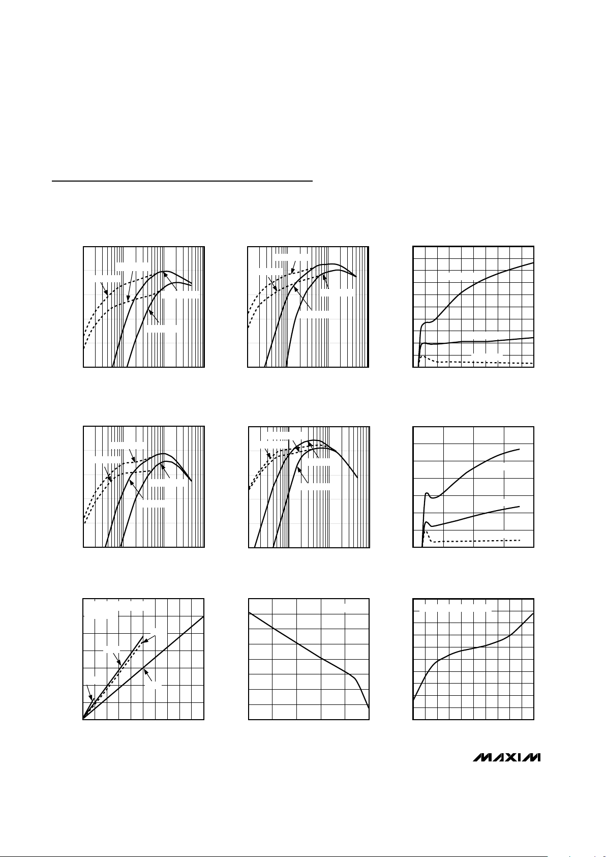
Typical Operating Characteristics
(Circuit of Figure 2, REG0 to REG5 outputs at POR states, V
OUT0
= 3.75V, V
OUT4
= 5.25V, V
OUT1
= V
OUT2
= V
OUT3
= V
OUT5
= 3.3V,
TA= +25°C, unless otherwise noted.)
1 10 100 1,000
MAX886
REG0 EFFICIENCY vs. LOAD CURRENT
(V
BATT
= 8.4V)
MAX886/88-01
LOAD CURRENT (mA)
EFFICIENCY (%)
100
50
70
60
80
90
PFM, 375kHz
PFM, 925kHz
PWM, 375kHz
PWM, 925kHz
1 10 100 1,000
MAX886
REG0 EFFICIENCY vs. LOAD CURRENT
(V
BATT
= 5.4V)
MAX886/88-02
LOAD CURRENT (mA)
EFFICIENCY (%)
100
50
70
60
80
90
PFM, 375kHz
PFM, 925kHz
PWM, 375kHz
PWM, 925kHz
0
2
1
4
3
6
5
7
9
8
10
2 4563 789 1110 12
MAX886
NO-LOAD BATTERY CURRENT
vs. BATTERY VOLTAGE
MAX886/88-03
BATTERY VOLTAGE (V)
BATTERY CURRENT (mA)
PWM, 375kHz
PWM, 925kHz
PFM MODE
1 10 100 1,000
MAX888
REG0 EFFICIENCY vs. LOAD CURRENT
(V
BATT
= 4.2V)
MAX886/88-04
LOAD CURRENT (mA)
EFFICIENCY (%)
100
50
70
60
80
90
PFM, 375kHz
PFM, 925kHz
PWM, 375kHz
PWM, 925kHz
0
40
20
60
120
100
80
140
0 20 40 60 80 100 120 140 160 180 200
DROPOUT VOLTAGE
vs. LOAD CURRENT
MAX886/88-07
LOAD CURRENT (mA)
DROPOUT VOLTAGE (mV)
V
IN1
= V
IN2
= V
IN5
= 3.3V
V
IN3
= 2.85V
REG3
REG1
REG5
REG2
1 10 100 1,000
MAX888
REG0 EFFICIENCY vs. LOAD CURRENT
(V
BATT
= 2.7V)
MAX886/88-05
LOAD CURRENT (mA)
EFFICIENCY (%)
100
50
70
60
80
90
PFM, 375kHz
PFM, 925kHz
PWM, 375kHz
PWM, 925kHz
0
2
1
4
3
6
5
7
24356
MAX888
NO LOAD BATTERY CURRENT
vs. BATTERY VOLTAGE
MAX886/88-06
BATTERY VOLTAGE (V)
BATTERY CURRENT (mA)
PWM, 375kHz
PWM, 925kHz
PFM MODE
5.12
5.14
5.16
5.18
5.20
5.22
5.24
5.26
5.28
0 20406080100
REG4 OUTPUT VOLTAGE
vs. LOAD CURRENT
MAX886/88-08
LOAD CURRENT (mA)
OUTPUT VOLTAGE (V)
V
IN4
= 3.75V
0
2
1
4
3
6
5
7
9
8
10
2 4563 789 1110 12
SHUTDOWN CURRENT
vs. BATTERY VOLTAGE
MAX886/88-09
BATTERY VOLTAGE (V)
SHUTDOWN CURRENT (µA)
R1, R2, R3 NOT CONNECTED

MAX886/MAX888
Wireless and Satellite Handset
Power-Management ICs
_______________________________________________________________________________________
7
70
0
0.01 0.1 1 10 100 1,000
REG1 POWER-SUPPLY REJECTION
RATIO vs. FREQUENCY
10
MAX886/88-10
FREQUENCY (kHz)
PSRR (dB)
30
20
40
60
50
V
OUT1
= 3.3V
I
OUT1
= 10mA
C
OUT1
= 2.2µF
70
0
0.01 0.1 1 10 100 1,000
REG2 POWER-SUPPLY REJECTION
RATIO vs. FREQUENCY
10
MAX886/88-11
FREQUENCY (kHz)
PSRR (dB)
30
20
40
60
50
V
OUT2
= 3.3V
I
OUT2
= 20mA
C
OUT2
= 2.2µF
400µs/div
REG0 TURN-ON DELAY
MAX886/88-12
I
OUT0
= 20mA
V
ON
(2V/div)
V
OUT0
(2V/div)
400µs/div
REG0 LINE-TRANSIENT RESPONSE
(PWM MODE)
MAX886/88-13
V
BATT
= 7V TO 8V, I
OUT0
= 500mA,
V
OUT0
= 3.75V, AC-COUPLED
V
BATT
(500mV/div)
V
OUT0
(100mV/div)
400µs/div
REG0 LOAD-TRANSIENT RESPONSE
(PWM MODE)
MAX886/88-16
V
BATT
= 5.4V, I
OUT0
= 0 TO 500mA,
V
OUT0
= 3.75V, AC-COUPLED
I
OUT0
(200mA/div)
V
OUT0
(100mV/div)
400µs/div
REG0 LINE-TRANSIENT RESPONSE
(PFM MODE)
MAX886/88-14
V
BATT
= 7V TO 8V, I
OUT0
= 5mA,
V
OUT0
= 3.75V, AC-COUPLED
V
BATT
(500mV/div)
V
OUT0
(100mV/div)
400µs/div
REG2 LINE-TRANSIENT RESPONSE
(IN2 CONNECTED TO OUT0)
MAX886/88-15
V
BATT
= 7V TO 8V, I
OUT2
= 5mA,
V
OUT2
= 3.3V, AC-COUPLED
V
BATT
(500mV/div)
V
OUT2
(100mV/div)
400µs/div
REG0 LOAD-TRANSIENT RESPONSE
(PFM MODE)
MAX886/88-17
V
BATT
= 5.4V, I
OUT0
= 0 TO 500mA,
V
OUT0
= 3.75V, AC-COUPLED
I
OUT0
(200mA/div)
V
OUT0
(100mV/div)
400µs/div
REG2 LOAD-TRANSIENT RESPONSE
(IN2 CONNECTED TO BATT)
MAX886/88-18
V
BATT
= V
IN2
= 5.4V, I
OUT2
= 0 TO 200mA,
V
OUT2
= 3.3V, AC-COUPLED
I
OUT2
(200mA/div)
V
OUT2
(100mV/div)
Typical Operating Characteristics (continued)
(Circuit of Figure 2, REG0 to REG5 outputs at POR states, V
OUT0
= 3.75V, V
OUT4
= 5.25V, V
OUT1
= V
OUT2
= V
OUT3
= V
OUT5
= 3.3V,
TA= +25°C, unless otherwise noted.)

MAX886/MAX888
Wireless and Satellite Handset
Power-Management ICs
8 _______________________________________________________________________________________
Pin Description
9 C+ Charge-Pump Capacitor Positive Connection
13 LBI
Low-Battery Detector Input. LBO goes low when V
LBI
drops below V
REF
. Connect LBI to the center of a
resistor voltage divider between BATT and GND.
15
LBO
Low-Battery Output. Open-drain output of the Low-Battery Detector Comparator. LBO is high impedance
when device is shutdown or V
LBI
> V
REF
. V
LBO
is low when V
LBI
< V
REF
. Typically, connect a 200kΩ pull-
up resistor between LBO and OUT2.
14 LBHYS
Low-Battery Detector Hysteresis Control. An open-drain output to set the hysteresis of the Low-Battery
Detector Comparator.
11 C- Charge-Pump Capacitor Negative Connection
12 DGND Digital Ground
10 IN4 Regulator 4 Power-Supply Input
5 REF Reference Output. Bypass with a 0.22µF capacitor to GND. REF can source up to 100µA.
7 BATT Supply Voltage Input. Bypass with a 0.1µF and a 10µF capacitor to PGND as close to BATT as possible.
8 OUT4 Charge-Pump Regulator 4 Output. Bypass with a 10µF, low-ESR capacitor to DGND.
6 GND Ground
3 OUT0
Switching Regulator 0 Output. Bypass with a 10µF, low-ESR capacitor to PGND. Up to 500mA is available
from OUT0.
4 CVL Low-Side Drive Bypass. Bypass with a 1µF capacitor to GND.
2 PGND Power Ground
NAME FUNCTION
1 LX Inductor Input. Drain of the internal p-channel MOSFET.
PIN
16
RESET
Reset Output. RESET remains low during initial power-up for 75ms after OUT2 is ready. RESET has an
internal 10kΩ pull-up resistor connected to OUT2. RESET is valid for V
BATT
down to 1V.
17 IN2 Linear Regulator 2 Power-Supply Input
18 OUT2
Linear Regulator 2 Output. Bypass with a 2.2µF, low-ESR capacitor to GND. Up to 200mA is available from
OUT2. The reset circuit monitors this voltage.
19 OUT3
Linear Regulator 3 Output. Bypass with a 1µF, low-ESR capacitor to GND. Up to 20mA is available from
OUT3.
20 IN3 Regulator 3 Power-Supply Input
21 IN5 Regulator 5 Power-Supply Input
22 OUT5
Linear Regulator 5 Output. Bypass with a 1µF, low-ESR capacitor to GND. Up to 100mA is available from
OUT5.
23 IN1 Regulator 1 Power-Supply Input

MAX886/MAX888
Wireless and Satellite Handset
Power-Management ICs
_______________________________________________________________________________________ 9
Pin Description (continued)
PIN FUNCTIONNAME
Linear Regulator 1 Output. Bypass with a 2.2µF, low-ESR capacitor to GND. Up to 100mA is available from
OUT1.
OUT124
Serial Interface Clock Input SCL29
Sync Input. Drive SYNC with a logic-level square wave to synchronize the internal oscillator. The capture
range for external clock is ±20% of the selected internal oscillator frequency. Drive SYNC low for more
than 10µs to force low-power PFM mode (standby mode). Drive SYNC high to force PWM mode.
SYNC30
High-Side Drive Bypass Input. Bypass CVH with a 0.1µF capacitor connected to IN0.CVH31
Regulator 0 Power-Supply Input. Connect to BATT. Source of the internal p-channel MOSFET. IN032
SCL
AB CDEFG HIJ
K
SDA
t
SU:STA
t
HD:STA
t
LOWtHIGH
t
SU:DAT
t
HD:DAT
t
SU:STO
t
BUF
A = START CONDITION
B = MSB OF ADDRESS CLOCKED INTO SLAVE
C = LSB OF ADDRESS CLOCKED INTO SLAVE
D = R/W BIT CLOCKED INTO SLAVE
E = SLAVE PULLS SMBDATA LINE LOW
L
M
F = ACKNOWLEDGE BIT CLOCKED INTO MASTER
G = MSB OF DATA CLOCKED INTO SLAVE (OP/SUS BIT)
H = LSB OF DATA CLOCKED INTO SLAVE
I = SLAVE PULLS SMBDATA LINE LOW
J = ACKNOWLEDGE CLOCKED INTO MASTER
K = ACKNOWLEDGE CLOCK PULSE
L = STOP CONDITION, DATA EXECUTED BY SLAVE
M = NEW START CONDITION
Figure 1. I2C-Compatible Serial-Interface Timing Diagram
Power-On Input. Pulse the ON pin low to turn on the IC. ON has an internal 16µA pull-up.ON
26
Serial Interface Data InputSDA28
ON Status Output. Push/pull logic output indicating the state of the ON input. The logic state of this pin
follows the logic state of the ON pin. The logic high output voltage is the output voltage of OUT2.
ONSTAT27
Power-Off Input. Drive OFF high before the start-up timer has expired in order to keep the IC powered on.
Drive OFF low to shut down the IC. OFF has an internal 100kΩ pull-down resistor to GND.
OFF
25

MAX886/MAX888
Wireless and Satellite Handset
Power-Management ICs
10 ______________________________________________________________________________________
BATT
IN1
CVH
LBI
LBHYS
GND
REF
SCL
IN0
LX
PGND
OUT0
IN2
OUT1
OUT2
LBO
RESET
OUT3
OUT4
IN3
OUT5
ONSTAT
MAX886
IN4
IN5
SDA
ON
OFF
SYNC
DGND
R1
1.1M
C4
0.1µF
C2
0.1µF
IN
4V TO 12V
C1
10µF
R2
562k
R3
23.3k
C5
0.22µF
CVL
C+
C-
C3
1µF
C6
0.22µF
C8
2.2µF
C7
2.2µF
OUT1
UP TO 100mA
OUT0
UP TO 500mA
D1
MBR0520L
L1
10µH
C9
1µF
C12
10µF
OUT3
UP TO 20mA
R5
200k
OUT4
5.25V UP TO 100mA
C10
1µF
OUT5
UP TO 100mA
OUT2
UP TO 200mA
C11
10µF
Figure 2a. Typical 2 Li+ or 5 to 6 Ni-Cell Application Circuit (MAX886)

MAX886/MAX888
Wireless and Satellite Handset
Power-Management ICs
______________________________________________________________________________________ 11
BATT
IN1
CVH
LBI
LBHYS
GND
REF
SCL
IN0
LX
PGND
OUT0
IN2
OUT1
OUT2
LBO
RESET
OUT3
OUT4
IN3
OUT5
ONSTAT
MAX888
IN4
IN5
SDA
ON
OFF
SYNC
DGND
R1
619k
C4
0.1µF
C2
0.1µF
IN
2.7V TO 5.5V
C1
10µF
R2
562k
R3
47.6k
C5
0.22µF
CVL
C+
C-
C3
1µF
C6
0.22µF
C8
2.2µF
C7
2.2µF
OUT1
UP TO 100mA
OUT0
UP TO 500mA
D1
MBR0520L
L1
10µH
C9
1µF
C12
10µF
OUT3
UP TO 20mA
R5
200k
OUT4
5.25V UP TO 100mA
C10
1µF
OUT5
UP TO 100mA
OUT2
UP TO 200mA
C11
10µF
Figure 2b. Typical 1 Li+ or 3 to 4 Ni-Cell Application Circuit (MAX888)

MAX886/MAX888
Wireless and Satellite Handset
Power-Management ICs
12 ______________________________________________________________________________________
Detailed Description
The MAX886/MAX888 contain one high-efficiency, stepdown DC-DC converter, four low-dropout linear regulators, and one regulated charge pump. The output
voltages of the switching regulator and the linear regulators are software-programmable through the serial interface. The regulated charge-pump output is factory set
at 5.25V. The devices also include reset and start-up
timers and a low-battery detect comparator (Figure 3).
500mA DC-DC Buck Regulator 0
Regulator 0 is a low-noise, step-down, synchronous
DC-DC converter that can source a minimum of
500mA. High operating frequency (up to 925kHz) minimizes output voltage ripple and reduces the size and
cost of external components. Guaranteed 100% dutycycle operation provides the lowest possible dropout
voltage, extending the useful life of the battery supply.
5
IN1
OUT1
IN2
OUT2
IN3
OUT3
IN5
OUT5
CVH
CVL
IN0
BATT
OUT0
C+
C-
PGND
IN4
OUT4
ONSTAT
LBO
ON1
ON2
ON5
ON0
LX
ON4
SDA
SCL
SYNC
RESET
ON
OFF
LBI
REF
LBHYS
DGND
LOGIC
DECODER
RESET AND
START UP
TIMER
REG4
CHARGE
PUMP
REGULATOR
OSCILLATOR
SWITCHING
REGULATOR
LINEAR
REG1
LINEAR
REG5
REF
DAC5
DAC0
DAC2
DAC1
LINEAR
REG2
DAC3
LINEAR
REG3
OUT2
10k
+
GND
ON2
Figure 3. Functional Diagram

MAX886/MAX888
Wireless and Satellite Handset
Power-Management ICs
______________________________________________________________________________________ 13
The serial interface programs V
OUT0
from 2.625V to
3.75V in 75mV steps for the MAX886 (Tables 1 and 2),
or from 1.527V to 3.027V in 100mV steps for the
MAX888 (Tables 1 and 3).
Regulator 0 operates in one of four preset frequencies,
from 375kHz to 925kHz, programmable through the
serial interface (Table 4).
For the device to power up properly, V
IN0
must be high
enough for REG0 to get into regulation. For the MAX886,
Regulator 0’s default voltage is 3.75V. Since the rest of
the regulators do not power up until Regulator 0 is
ready, V
IN0
must be greater than approximately 4V for
the device to power up properly. The Regulator 0 default
voltage for the MAX888 is 2.027V, so the minimum V
IN0
required to start up is limited by the minimum operating
voltage range (2.7V). After power-up, the device operates until V
BATT
drops below V
UVLOF
(undervoltage
lockout falling threshold).
Sync Mode
The SYNC input allows the MAX886/MAX888 to synchronize with an external clock applied to SYNC, ensuring that switching harmonics are kept away from
sensitive IF bands. The SYNC detector triggers on
SYNC’s falling edge.
PWM Mode
Regulator 0 is in PWM mode when SYNC is connected to
CVL or driven to a logic-high voltage. Two internal switches operate at a preset frequency even when there is no
load. The P-channel MOSFET turns on to charge the
inductor until the error comparator or current-limit comparator turns it off. The N-channel MOSFET then turns on
to discharge the inductor. To prevent the output from
soaring with no load in PWM mode, the N-channel switch
stays on long enough to allow the inductor current to go
negative. Once the N-channel switch turns off, the voltage
at LX rises (rings) until the next cycle when the P-channel
switch turns on again. As the load increases and the
inductor enters continuous conduction, ringing is no
longer present and the LX waveform looks like a square
wave whose duty cycle depends on the input and output
voltages. As the input voltage approaches the same level
as the output voltage, the P-channel switch stays on
100% of the time, providing the lowest possible dropout.
PFM Mode
Regulator 0 operates in PFM mode when SYNC is driven to a logic low voltage or connected to GND. When
V
OUT0
drops below the regulation threshold, the Pchannel switch turns on to charge the inductor until the
error comparator or current-limit comparator turns it off.
At light loads, the N-channel then turns on to discharge
the inductor until the current in the inductor reaches
zero. In PFM mode, the inductor current does not go
negative to discharge the output. At no-load there is a
long period between pulses of inductor current. As the
load current increases, the period between pulses
becomes shorter until the pulses become continuous. At
load currents above this point, Regulator 0 automatically
switches to PWM mode, and the V
LX
waveform looks like
a square wave whose duty cycle depends on the input
and output voltages. As the input voltage approaches
the same level as the output voltage, the P-channel
switch stays on 100% of the time, providing the lowest
possible dropout. It is typically more efficient to use the
PFM mode when the load current is less than 100mA.
100mA LDO Regulator 1
Regulator 1, a low-dropout linear regulator, sources a
minimum of 100mA and operates from voltages at IN1
of up to 12V. The serial interface programs V
OUT1
from
2.7V to 4.95V in 75mV steps for the MAX886 (Tables 1
and 2), or from 1.25V to 3.50V in 150mV steps for the
MAX888 (Tables 1 and 3). IN1 may be powered from
the battery, OUT0, or any other voltage source.
200mA LDO Regulator 2
Regulator 2, a low-dropout linear regulator, sources a
minimum of 200mA. The serial interface programs V
OUT2
from 2.175V to 3.3V in 75mV steps for the MAX886 (Tables
1 and 2), or from 1.527V to 3.027V in 100mV steps for the
MAX888 (Tables 1 and 3). IN2 may be powered from the
battery, OUT0, or any other voltage source less than 5.5V.
20mA LDO Regulator 3
Regulator 3, a low-dropout linear regulator, sources a
minimum of 20mA. The serial interface programs V
OUT3
to one of four different output voltages: 0V, 2.85V, 4.65V,
or V
OUT2
(Tables 1 and 5). Although this is a generalpurpose output, OUT3 is intended for the SIM supply. IN3
may be powered from OUT4 or from any regulated 5V
supply.
When programmed to 0V or V
OUT2
, OUT3 is either actively
discharged to GND (for 0V mode) or connected to OUT2
(for V
OUT2
), and Regulator 3 is disabled to conserve
power.
100mA Charge-Pump Regulator 4
Regulator 4, a regulated charge pump, generates 5.25V
and delivers up to 100mA. An oscillator synchronized to the
PWM clock regulates OUT4 to minimize noise. It operates
at one-half the frequency of the PWM oscillator to ensure
50% duty-cycle outputs. IN4 may be powered from the battery, OUT0, or any other voltage source less than 5.5V.
To save space and cost, use a small ceramic flying
capacitor. See Table 6 for recommended flying capacitor values.

MAX886/MAX888
Wireless and Satellite Handset
Power-Management ICs
14 ______________________________________________________________________________________
100mA LDO Regulator 5
Regulator 5, a low-dropout linear regulator, can source a
minimum of 100mA. The output voltage is programmable
from 2.175V to 3.3V in 75mV steps for the MAX886
(Tables 1 and 2), or 1.25V to 3.50V in 150mV steps for the
MAX888 (Tables 1 and 3). IN5 may be powered from the
battery, OUT0, or any other voltage source less than 5.5V.
Control Data Byte
The control byte is eight bits long (four address bits,
four data bits). Each regulator has a DAC that sets the
output regulation voltage. Control codes are summarized in Table 1.
Table 1. Control Data Byte
Table 2. MAX886 Output Voltage Settings
Note: The output voltage of each regulator can be set independently. The POR states are in boldface.
0
0
0
ADDRESS
1
0
0
1 0
DAC0
DATA
DAC1
0 DAC50OUT5 Output Voltage
0
0
0
1
1
1
A2
DAC3
DAC2
f
OSC
A0A1
FUNCTION
D2
D0
LSB
0OUT2 Output Voltage
0OUT0 Output Voltage
0OUT3 Output Voltage, f
OSC
0OUT1 Output Voltage
D1
1
D3
10
A3
MSB
ON4 ON1ON2ON5
1
1
0
1
1
1
X
X
ON0
X
X
X
X
X
0OUT0 On/Off Control
0Not Available
0OUT1, 2, 4, 5 On/Off Control
X XX X XXX1Not Available
2.70
2.85
2.625
2.700
0
0
0
1
0
0
0
DACX DATA
0
3.00
3.15
REGULATOR OUTPUT VOLTAGE (V)
2.775
2.850
0
0
0
2.175
1
1
1
2.250
0
0
2.325
2.400
3.30
3.45
2.925
3.000
1
1
0
1
0
0
0
0
3.60
3.75
OUT1
3.075
3.150
1
1
0
2.475
1
1
1
2.550
0
0
2.625
2.700
3.90
4.05
OUT0 D2
3.225
3.300
0
0
0
1
0
0
1
1
4.20
4.35
D0D1
3.375
3.450
0
0
0
2.775
1
1
1
2.850
1
1
2.925
3.000
4.50
4.65
D3OUT5
3.525
3.600
1
1
0
1
0
0
1
1
4.80
4.95
OUT2
3.675
3.750
1
1
0
3.075
1
1
1
3.150
1
1
3.225
3.300
2.175
2.250
2.325
2.400
2.475
2.550
2.625
2.700
2.775
2.850
2.925
3.000
3.075
3.150
3.225
3.300

MAX886/MAX888
Wireless and Satellite Handset
Power-Management ICs
______________________________________________________________________________________ 15
Low-Battery Detector
A low-battery comparator detects low-battery conditions. The trip threshold is internally set to V
REF
(1.25V
typ). LBHYS sets the hysteresis with external resistors.
LBO and LBHYS have open-drain outputs. The externally set low-battery threshold must be higher than the
UVLOF threshold (2.45V typical).
Set the threshold and hysteresis by connecting resistors R1 (between BATT and LBI), R2 (between LBI and
LBHYS), and R3 (LBHYS and GND) (Figure 2).
After choosing the upper and lower thresholds, calculate the resistor values as follows:
1) Choose a value for R1. Typical values range from
500kΩ to 1.5MΩ.
2) Calculate R2:
3) Calculate R3:
R3
R2 V V R1 V
V V
THF REF REF
REF THF
=
−
()
−
−
⋅
R
R
V
V
THR
REF
2
1
1
–
=
Table 3. MAX888 Output Voltage Settings
Table 5. OUT3 Output Voltage Setting
Table 4. Oscillator Frequency Setting
0
0
0
1
0
0
0
0
0
0
0
1.25
1
1
1
1.40
0
0
1.55
1.70
1
1
0
1
0
0
0
0
1
1
0
1.85
1
1
1
2.00
0
0
2.15
2.30
0
0
0
1
0
0
1
1
0
0
0
2.45
1
1
1
2.60
1
1
2.75
2.90
1
1
0
1
0
0
1
1
1
1
0
3.05
1
1
1
3.20
1
1
3.35
3.50
1.527
1.627
1.727
1.827
1.927
2.027
2.127
2.227
2.327
2.427
2.527
2.627
2.727
2.827
2.927
3.027
1.25
1.40
1.55
1.70
1.85
2.00
2.15
2.30
2.45
2.60
2.75
2.90
3.05
3.20
3.35
3.50
1.527
1.627
1.727
1.827
1.927
2.027
2.127
2.227
2.327
2.427
2.527
2.627
2.727
2.827
2.927
3.027
REGULATOR OUTPUT VOLTAGE (V) DACX DATA
OUT1 OUT0 D2 D0D1D3OUT5 OUT2
Note: The output voltage of each regulator can be set independently. The POR states are in boldface.
0
0
X
X
0
1
D3 D1D2
ADDRESS 03h
DATA
0V (REG3 Off)
2.85V
X
X
D0
1
1
X
X
0
1
X
X
4.65V
VOUT2 (REG3 Off)
X
X
0
0
X
X
0
1
D0
X
X
1
1
X
X
0
1
D3 D1D2
670
925
ADDRESS 03h DATA
f
OSC
(kHz)
375
535
Note: The POR states are in boldface.
Note: The POR states are in boldface.

MAX886/MAX888
Wireless and Satellite Handset
Power-Management ICs
16 ______________________________________________________________________________________
For example:
V
REF
= 1.25V
V
THF
= falling threshold = 2.52V
V
HYS
= hysteresis = 0.1V
V
THR
= rising threshold = V
THF
+ V
HYS
= 2.62V
R1 = 619kΩ (1%)
R2 = 562kΩ (1%)
R3 = 47.6kΩ (1%)
Power-On Sequence
(Including
RREESSEETT
and Start-Up Timers)
Drive ON low to begin the power-up sequence. To reduce
overall system cost and complexity, the MAX886/MAX888
incorporate RESET and start-up timers with the power-on
sequence.
The MAX886/MAX888 turn on the reference when ON
goes low. Once the reference is fully powered up, if the
input voltage exceeds the internal undervoltage-lockout
threshold (UVLOR), Regulator 0 turns on. Once OUT0
is in regulation, OUT2 and OUT4 turn on. Once OUT2 is
in regulation, OUT1 and OUT5 turn on and the 75ms
reset timer begins. RESET remains low from the time
OUT2 is valid until the reset timer times out. After the
reset period expires, a 50ms start-up timer begins. The
MAX886/MAX888 shut down if the external logic or controller fails to drive OFF high before the start-up timer
expires. Drive OFF high to continue operation. Driving
OFF low turns off the IC.
There is no required sequence to power off any regulator after the device has turned on. Regulators can be
powered off selectively by sending the correct code
through the serial interface (Table 1).
ONSTAT Output
ONSTAT is a logic output that follows ON. Connect
ONSTAT to the external logic or controller to sense
when the ON pin has been brought low to request shutdown. This allows easy implementation of a one-button
on/off control scheme (Figure 4).
Thermal Overload Protection
An internal thermal sensor shuts the MAX886/MAX888
down when the maximum temperature limit is exceeded
(160°C typical).
I2C-Compatible Serial Interface
Use an I2C-compatible serial interface to turn the
MAX886/MAX888 on and off, as well as control each
regulator’s output voltage and program the DC-DC
converter and charge pump’s oscillator frequency. Use
standard I2C-compatible receive-byte commands to
program the IC. This part is always a slave to the bus
master. The chip address is 1001 111.
POR State
The power-on reset state of all the DAC and frequency
registers is 0Fh, except for DAC1 which is 04h. The
power-on reset state of the ONX bits is 1 (Table 1). The
power-on voltage for each regulator is shown in bold in
Tables 2, 3, and 5.
Applications Information
Inductor Selection
The essential parameters for inductor selection are
inductance and current rating. The MAX886/MAX888
operate with a wide range of inductance values. In many
applications, values between 10µH and 68µH take best
advantage of the controller’s high switching frequency.
Calculate the minimum inductance value using the simplified equation:
where I
PEAK
is the peak inductor current (0.9A) and
f
OSC
is the switching frequency.
For example, for a 6V battery voltage, a desired V
OUT0
is 3.3V, the oscillator frequency is 375kHz, and 15µH is
the minimum inductance required.
Diode Selection
The MAX886/MAX888’s high switching frequency
demands a high-speed rectifier. Schottky diodes, such
as the 1N5817–1N5822 family or surface-mount
MBR0520L series are recommended. Ultra-high-speed
rectifiers with reverse recovery times around 50ns or
L
4V V
I f V / V
MIN
BATT MAX OUT0
PEAK OSC BATT OUT0
()
()
=
−
()
⋅⋅
MAX886
MAX888
µC
RESET
OUT2
ONSTAT
ON
OFF
10k
Figure 4. One-Button On/Off Control with ONSTAT

MAX886/MAX888
Wireless and Satellite Handset
Power-Management ICs
______________________________________________________________________________________ 17
faster, such as the MUR series, are acceptable. Ensure
that the diode’s peak current rating exceeds the peak
current (1A), and that its breakdown voltage exceeds
V
BATT
. Schottky diodes are preferred for heavy loads
due to their low forward voltage, especially in low-voltage applications.
Capacitor Selection
Choose filter capacitors to service input and output
peak currents with acceptable voltage ripple. The
capacitor’s equivalent series resistance (ESR) is a
major contributor to ripple; therefore, low-ESR capacitors are recommended for OUT1–OUT5. A tantalum
capacitor is recommended for OUT0 (refer to Figures
2a and 2b, and Table 6).
The input filter capacitor reduces peak currents drawn
from the power source, and reduces noise and voltage
ripple on the input, which are caused by the circuit’s
switching action. Since the current from the battery is
interrupted each time the PMOS switch opens, pay special attention to the ripple current rating of the input filter
capacitor and use a low-ESR capacitor. Choose input
capacitors with working voltage ratings higher than the
maximum input voltage. Input capacitors prevent spikes
and ringing on the power source from obscuring the
current-feedback signal and causing jitter.
Bypass REF with 0.22µF to GND. The capacitor should
be placed within 0.2 inches of the IC, next to REF, with
a direct trace to GND.
Table 6. OUT0 and OUT4 Regulator
Component Recommendations
Table 7. Component Suppliers
Layout Considerations
High-frequency switching regulators are sensitive to PC
board layout. Poor layout introduces switching noise
into the current and voltage-feedback signals, resulting
in jitter, instability, or degraded performance. Place the
anode of the Schottky diode and the ground pins of the
input and output capacitors close together, and route
them to a common “star-ground” point. Place components and route ground paths so as to prevent high
currents from causing large voltage gradients between
the ground pin of the output filter capacitor, the controller IC, and the reference bypass capacitor. Keep
the extra copper on the component and solder sides of
the PC board rather than etching it away, and connect
it to ground for use as a pseudo-ground plane. Refer to
the MAX886/MAX888 evaluation kit for a two-layer PC
board layout example.
925
670
0.22
0.33
10
15
10
15
C12
(µF)
535
375
0.47
1
22
33
22
33
f
OSC
(kHz)
C6
(µF)
L1
(µH)
10
15
22
33
C11
(µF)
AVX 803-946-0690
Coilcraft 847-639-6400
803-626-3123
516-241-7876
847-639-1469
605-668-4131
Coiltronics
Dale
516-241-9339
605-665-1627
COMPANY FAXPHONE
Internal Rectifier 310-322-3331
Motorola 602-303-5454
310-322-3332
619-661-6835
602-994-6430
408-988-8000
Sanyo
Sprague
619-661-1055
408-970-3950
847-956-0666Sumida 847-956-0702

MAX886/MAX888
Wireless and Satellite Handset
Power-Management ICs
18 ______________________________________________________________________________________
Chip Information
TRANSISTOR COUNT: 2042
MAX886
MAX888
TOP VIEW
32 28
293031
25
26
27
CVH
SYNC
SCL
SDA
IN0
ONSTATONOFF
10
13
15
14
1611 12
9
C+
C-
IN4
LBI
DGND
LBO
LBHYS
RESET
17
18
19
20
21
22
23
IN1
24 OUT1
OUT5
IN5
IN3
OUT3
OUT2
IN2
2
3
4
5
6
7
8OUT4
BATT
GND
REF
CVL
OUT0
PGND
1LX
Pin Configuration

MAX886/MAX888
Wireless and Satellite Handset
Power-Management ICs
______________________________________________________________________________________ 19
Package Information
TQFPPO.EPS

MAX886/MAX888
Wireless and Satellite Handset
Power-Management ICs
20 ______________________________________________________________________________________
NOTES
 Loading...