

Page 1
General Description
The MAX8887/MAX8888 low-dropout linear regulators
operate from a 2.5V to 5.5V input and deliver up to
300mA continuous (500mA pulsed) current. The
MAX8887 is optimized for low-noise operation, while the
MAX8888 includes an open-drain POK ouput flag. Both
regulators feature exceptionally low 100mV dropout at
200mA. These devices are available in a variety of preset output voltages in the 1.5V to 3.3V range.
An internal PMOS pass transistor allows the low 55µA
supply current to remain independent of load, making
these devices ideal for portable battery-powered equipment such as personal digital assistants (PDAs), cellular phones, cordless phones, and notebook computers.
Other features include a micropower shutdown mode,
short-circuit protection, thermal shutdown protection,
and an active-low open-drain power-OK (POK) output
that indicates when the output is out of regulation. The
MAX8887/MAX8888 are available in a thin 5-pin SOT23
package that is only 1mm high.
________________________Applications
Notebook Computers
Wireless Handsets
PDAs and Palmtop Computers
Digital Cameras
PCMCIA Cards
Hand-Held Instruments
Features
♦ Guaranteed 300mA Output Current (500mA for
Pulsed Loads)
♦ Low 100mV Dropout at 200mA Load
♦ POK Output (MAX8888)
♦ 42µV
RMS
Output Noise (MAX8887)
♦ Preset Output Voltages (1.5V, 1.8V, 2.85V, and
3.3V)
♦ 55µA No-Load Supply Current
♦ Thermal Overload and Short-Circuit Protection
♦ Foldback Output Current-Limit Protection
♦ 60dB PSRR at 1kHz
♦ 0.1µA Shutdown Current
♦ Thin 5-Pin SOT23 Package, 1mm High
MAX8887/MAX8888
Low-Dropout, 300mA Linear Regulators in SOT23
________________________________________________________________ Maxim Integrated Products 1
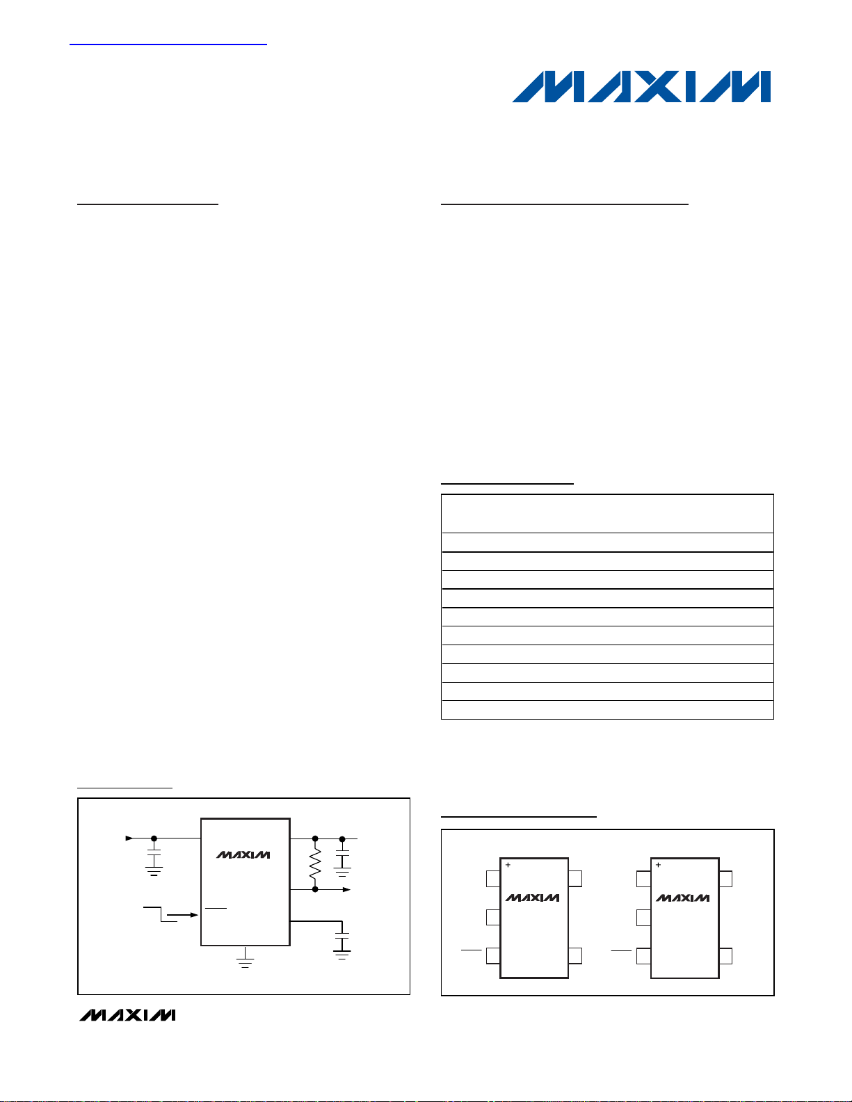
Pin Configurations
MAX8887
MAX8888
ON
OFF
INPUT
2.5V TO 5.5V
IN
SHDN
GND
(BP)
POK
OUT
V
OUT
300mA
C
IN
2.2μF
C
OUT
2.2μF
C
BP
0.01μF
( ) ARE FOR MAX8887 ONLY.
Typical Operating Circuit
19-1859; Rev 3; 11/06
Ordering Information
*Other versions (xy) between +1.5 and +3.3V are available in
100mV increments. Contact factory for other versions. Minimum
order quantity is 25,000 units.
+Denotes lead-free availability.
For pricing, delivery, and ordering information, please contact Maxim/Dallas Direct! at
1-888-629-4642, or visit Maxim’s website at www.maxim-ic.com.
查询MAX8887EZK15供应商
PART
M A X8 8 8 7 E Z K15+ T -40°C to +85°C 5 SOT23-5 ADQD
MAX8887EZK18+ T -40°C to +85°C 5 SOT23-5 ADPX
MAX8887EZK29+ T -40°C to +85°C 5 SOT23-5 ADPY
MAX8887EZK33+ T -40°C to +85°C 5 SOT23-5 ADPZ
MAX8887EZKxy+ T* -40°C to +85°C 5 SOT23-5 —
M A X8 8 8 8 E Z K15+ T -40°C to +85°C 5 SOT23-5 ADQE
MAX8888EZK18+ T -40°C to +85°C 5 SOT23-5 ADQA
MAX8888EZK29+ T -40°C to +85°C 5 SOT23-5 ADQB
MAX8888EZK33+ T -40°C to +85°C 5 SOT23-5 ADQC
MAX8888EZKxy+ T* -40°C to +85°C 5 SOT23-5 —
TEMP
RANGE
PINPACKAGE
MARK
TOP
TOP VIEW
15OUTIN
MAX8887
2
GND
34
BPSHDN
15OUTIN
MAX8888
2
GND
34
POKSHDN
Page 2
MAX8887/MAX8888
Low-Dropout, 300mA Linear Regulators in SOT23
2 _______________________________________________________________________________________
ABSOLUTE MAXIMUM RATINGS
ELECTRICAL CHARACTERISTICS
(VIN= V
OUT
+ 1V, SHDN = IN, TA = -40°C to +85°C, unless otherwise noted.) (Note 1)
Stresses beyond those listed under “Absolute Maximum Ratings” may cause permanent damage to the device. These are stress ratings only, and functional
operation of the device at these or any other conditions beyond those indicated in the operational sections of the specifications is not implied. Exposure to
absolute maximum rating conditions for extended periods may affect device reliability.
IN, SHDN, POK, to GND...........................................-0.3V to +7V
OUT, BP to GND ............................................-0.3 to (V
IN
+ 0.3V)
Output Short-Circuit Duration.....................................Continuous
Continuous Power Dissipation (T
A
= +70°C)
5-Pin SOT23 (derate 9.1mW/°C above +70°C)............727mW
Operating Temperature Ranges..........................-40°C to +85°C
Junction Temperature......................................................+150°C
Storage Temperature Range .............................-65°C to +150°C
Lead Temperature (soldering, 10s) .................................+500°C
Input Voltage V
Input Undervoltage Lockout
Output Voltage Accuracy
Maximum Output Current
Current Limit
Ground-Pin Current
Dropout Voltage (Note 2) V
Line Regulation
Output Noise
PSRR
PARAMETER SYMBOL CONDITIONS MIN TYP MAX UNITS
IN
V
rising
IN
(2% typical hysteresis)
TA = +25°C, I
I
= 100µA to 300mA,
OUT
= 0°C to +85°C
T
A
= 100µA to 300mA -3 +3
I
OUT
Continuous 300
10ms pulse 500
V
= 0
OUT
> 93% of nominal value 420
V
OUT
No load 55 100
= 300mA 65
I
OUT
= +3.3V
OUT
V
= 2.5V or (V
IN
I
= 5mA
OUT
MAX8887
MAX8888
MAX8887
MAX8888
2.5 5.5 V
2.15 2.4 V
= 100mA -1.2 +1.2
OUT
-2 +2
300
I
= 1mA
OUT
I
= 200mA 100 200
OUT
I
= 300mA 150
OUT
+ 0.4V) to 5.5V,
OUT
10Hz to 100kHz, C
C
= 2.2µF, ESR
OUT
10Hz to 100kHz, C
ESR
f < 1kHz, C
C
OUT
f < 1kHz, C
ESR
< 0.1Ω
COUT
= 0.01µF,
BP
= 4.7µF, ESR
OUT
< 0.1Ω
COUT
= 2.2µF,
= 0.01µF,
BP
COUT
= 2.2µF,
OUT
COUT
-0.15 0 0.15 %/V
< 0.1Ω
< 0.1Ω
0.5
42
360
60
40
µV
%
mA
mA
µA
mV
RMS
dB
Page 3
MAX8887/MAX8888
Low-Dropout, 300mA Linear Regulators in SOT23
_______________________________________________________________________________________ 3
ELECTRICAL CHARACTERISTICS (continued)
(VIN= V
OUT
+ 1V, SHDN = IN, TA = -40°C to +85°C, unless otherwise noted.) (Note 1)
Note 1: All parts are 100% tested at T
A
= +25°C. Limits over the operating temperature range are guaranteed by design.
Note 2: Typical and maximum dropout voltage for different output voltages are shown in the Typical Operating Characteristics
curve.
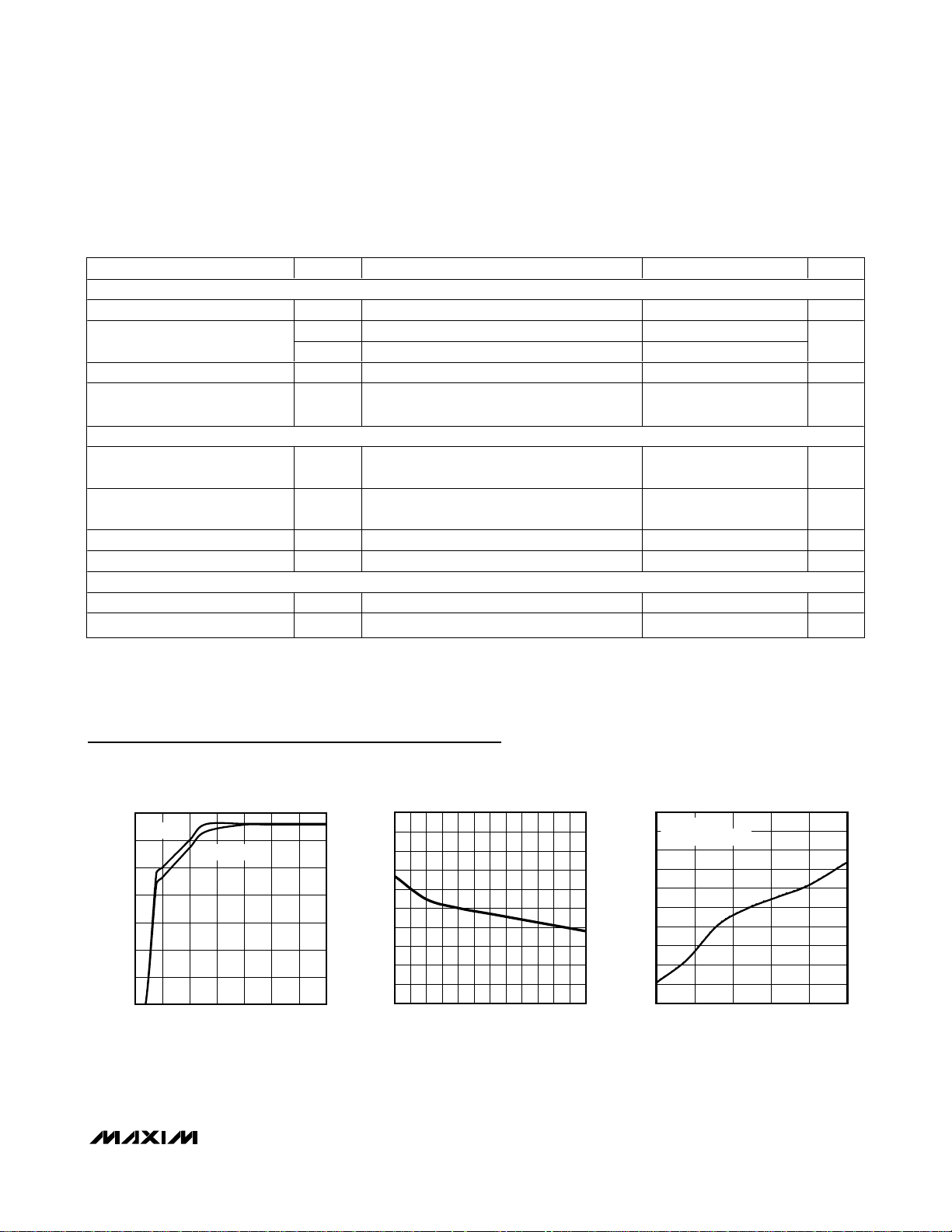
Typical Operating Characteristics
(Typical Operating Circuit, TA = +25°C, unless otherwise noted.)
0
1.0
0.5
2.0
1.5
3.0
2.5
3.5
2.0 3.0 3.52.5 4.0 4.5 5.0 5.5
OUTPUT VOLTAGE vs. INPUT VOLTAGE
MAX8887/8 toc01
INPUT VOLTAGE (V)
OUTPUT VOLTAGE (V)
I
OUT
= 0
I
OUT
= 300mA
-1.0
-0.6
-0.8
0.0
-0.2
-0.4
0.2
0.4
0.8
0.6
1.0
10050 150 200 250 300
OUTPUT VOLTAGE ACCURACY
vs. LOAD CURRENT
MAX8887/8 toc02
LOAD CURRENT (mA)
% DEVIATION (%)
0
-0.05
-0.02
-0.03
-0.04
-0.01
0.0
0.01
0.02
0.03
0.04
0.05
-40 10-15 35 60 85
OUTPUT VOLTAGE ACCURACY
vs. TEMPERATURE
MAX8887/8 toc03
TEMPERATURE (°C)
% DEVIATION
I
OUT
= 0
V
IN
= V
OUT
+ 500mV
SHUTDOWN
Shutdown Supply Current SHDN = GND, VIN = 5.5V 0.1 2 µA
SHDN Input Threshold
SHDN Input Bias Current SHDN = IN or GND 10 100 nA
OUT Discharge Resistance in
Shutdown
POK (MAX8888 ONLY)
POK Trip Level, Referred to OUT
Set Point
Operating IN Voltage Range for
Valid POK
POK Output Voltage Low V
POK Output Leakage Current V
THERMAL PROTECTION
Thermal Shutdown Temperature 170 °C
Thermal Shutdown Hysteresis 20 °C
PARAMETER SYMBOL CONDITIONS MIN TYP MAX UNITS
V
V
2.5V ≤ VIN ≤ 5.5V 1.6
IH
2.5V ≤ VIN ≤ 5.5V 0.6
IL
SHDN = GND 650 1100 Ω
V
falling
OUT
(1% typical hysteresis)
90 92.5 95 %
1.0 5.5 V
I
OL
= 1mA 0.1 V
SINK
= 5.5V, SHDN = IN 100 nA
POK
V
Page 4

MAX8887/MAX8888
Low-Dropout, 300mA Linear Regulators in SOT23
4 _______________________________________________________________________________________
Typical Operating Characteristics (continued)
(Typical Operating Circuit, TA = +25°C, unless otherwise noted.)
DROPOUT VOLTAGE vs. LOAD CURRENT
160
(mV)
140
120
100
TA = +85°C
TA = +25°C
MAX8887/8 toc04
80
DROPOUT
V
60
40
TA = -40°C
20
0
0 10050 150 200 250 300
LOAD CURRENT (mA)
GROUND-PIN CURRENT vs. LOAD CURRENT
100
VIN = 5.5V
80
60
VIN = 3.8V
40
GROUND-PIN CURRENT (μA)
20
0
0 10050 150 200 250 300
LOAD CURRENT (mA)
MAX8887/8 toc07
DROPOUT VOLTAGE vs. OUTPUT VOLTAGE
300
250
200
MAXIMUM
(mV)
150
DROPOUT
V
100
TYPICAL
50
0
2.5 2.7 2.9 3.1 3.3
V
OUT
(V)
I
OUT
GROUND-PIN CURRENT vs. TEMPERATURE
70
I
= 0
OUT
68
= V
IN
+ 500mV
OUT
TEMPERATURE (°C)
V
66
64
62
60
58
56
GROUND-PIN CURRENT (μA)
54
52
50
-40 10-15 35 60 85
= 200mA
MAX8887/8 toc05
MAX8887/8 toc08
GROUND-PIN CURRENT vs. INPUT VOLTAGE
150
125
100
I
= 300mA
LOAD
75
50
GROUND-PIN CURRENT (μA)
I
LOAD
25
0
0 1.0 2.0 3.0 4.0 5.0
INPUT VOLTAGE (V)
POWER-SUPPLY REJECTION RATIO
vs. FREQUENCY
70
60
C
= 2.2μF
OUT
= 0.01μF
C
BP
50
40
PSRR (dB)
30
20
V
= 3.30V
OUT
10
= 30mA
I
LOAD
0
0.01 0.1 1 10 100 1000
MAX8887 ONLY
FREQUENCY (kHz)
MAX8887/8 toc06
= 0
MAX8887/8 toc09
MAX8887
OUTPUT NOISE DC TO 1MHz
V
= 1.8V, VIN = 3.8V, I
OUT
LOAD
40ms/div
= 15mA
MAX8887/8 toc10
V
OUT
50μV/div
I
OUT
V
OUT
LOAD-TRANSIENT RESPONSE
MAX8887/8 toc11
V
OUT
V
IN
10μs/div
= 3.3V
= 3.8V
300mA
10mA
50mV/div
AC-COUPLED
Page 5

MAX8887/MAX8888
Low-Dropout, 300mA Linear Regulators in SOT23
_______________________________________________________________________________________ 5
Pin Description
Typical Operating Characteristics (continued)
(Typical Operating Circuit, TA = +25°C, unless otherwise noted.)
LOAD-TRANSIENT RESPONSE
V
I
OUT
V
OUT
SHDN
V
NEAR DROPOUT
10μs/div
SHUTDOWN WAVEFORM
OUT
MAX8887/8 toc12
V
OUT
V
IN
MAX8887/8 toc14
= 3.3V
= 3.4V
300mA
10mA
50mV/div
AC-COUPLED
2V/div
LINE-TRANSIENT RESPONSE
V
IN
V
OUT
100μs/div
POK WAVEFORM
V
= 3.3V, R
V
IN
V
OUT
OUT
I
LOAD
V
LOAD
MAX8887/8 toc13
= 3.3V
OUT
= 100mA
MAX8887/8 toc15
= 100Ω
4.5V
4V
20mV/div
AC-COUPLED
2V/div
2V/div
V
OUT
= 3.3V, R
LOAD
= 10Ω
20μs/div
1V/div
DC-COUPLED
V
POK
20ms/div
MAX8887 MAX8888 NAME FUNCTION
11IN
Regulator Input. Supply voltage can range from 2.5V to 5.5V. Bypass with 2.2µF
capacitor to GND (see the Capacitor Selection and Regulator Stability section).
2 2 GND Ground
33SHDN
Active-Low Shutdown Input. A logic low reduces the supply current to below 0.1µA.
In shutdown, POK and OUT are driven low. Connect to IN for normal operation.
Open-Drain Active-Low POK Output. POK remains low while the output voltage (V
—4POK
below the reset threshold. Connect a 100kΩ pullup resistor to OUT to obtain a logic level
output. POK is driven low in shutdown. If not used, leave this pin unconnected.
4 — BP Reference Bypass. Bypass with a low-leakage 0.01µF ceramic capacitor.
5 5 OUT
Regulator Output. Sources up to 300mA guaranteed. Bypass with 2.2µF (<0.2Ω typical
ESR) ceramic capacitor to GND.
2V/div
) is
OUT
Page 6

Detailed Description
The MAX8887/MAX8888 are low-dropout, low-quiescent-current linear regulators designed primarily for
battery-powered applications. The devices supply
loads up to 300mA and are available in several fixed
output voltages in the 1.5V to 3.3V range. The
MAX8887 is optimized for low-noise operation, while
the MAX8888 includes an open-drain POK output flag.
As illustrated in Figure 1, the MAX8888 consists of a
1.25V reference, error amplifier, P-channel pass transistor, and internal feedback voltage divider.
Internal P-Channel Pass Transistor
The MAX8887/MAX8888 feature a 0.5Ω P-channel
MOSFET pass transistor. Unlike similar designs using
PNP pass transistors, P-channel MOSFETs require no
base drive, which reduces quiescent current. PNPbased regulators also waste considerable current in
dropout when the pass transistor saturates and use
high base drive currents under large loads. The
MAX8887/MAX8888 do not suffer from these problems
and consume only 55µA of quiescent current under
heavy loads as well as in dropout.
Output Voltage Selection
The MAX8887/MAX8888 are supplied with various factory-set output voltages ranging from 1.5V to 3.3V. The
part number’s two-digit suffix identifies the nominal output voltage. For example, the MAX8887EZK33 has a
preset output voltage of 3.3V (see the Ordering Infor-
mation).
Shutdown
Drive SHDN low to enter shutdown. During shutdown,
the output is disconnected from the input and supply
current drops to 0.1µA. When in shutdown, POK and
OUT are driven low. SHDN can be pulled as high as
6V, regardless of the input and output voltages.
Power-OK Output
The power-OK output (POK) pulls low when OUT is less
than 93% of the nominal regulation voltage. Once OUT
exceeds 93% of the nominal voltage, POK goes high
impedance. POK is an open-drain N-channel output.
To obtain a logic level output, connect a pullup resistor
from POK to OUT. A 100kΩ resistor works well for most
applications. POK can be used as a power-on-reset
(POR) signal to a microcontroller (µC) or to drive other
logic. Adding a capacitor from POK to ground creates
POK delay. When the MAX8887 is shut down, POK is
held low independent of the output voltage. If unused,
leave POK grounded or unconnected.
Current Limit
The MAX8887/MAX8888 monitor and control the pass
transistor’s gate voltage, limiting the output current to
0.8A (typ). This current limit is reduced to 500mA (typ)
when the output voltage is below 93% of the nominal
value to provide foldback current limiting.
Thermal Overload Protection
Thermal overload protection limits total power dissipation in the MAX8887/MAX8888. When the junction temperature exceeds T
J
=+170°C, a thermal sensor turns
off the pass transistor, allowing the device to cool. The
thermal sensor turns the pass transistor on again after
the junction temperature cools by 20°C, resulting in a
pulsed output during continuous thermal overload conditions. Thermal overload protection protects the
MAX8887/MAX8888 in the event of fault conditions. For
continuous operation, do not exceed the absolute maximum junction-temperature rating of T
J
=+150°C.
Operating Region and Power Dissipation
The MAX8887/MAX8888’s maximum power dissipation
depends on the thermal resistance of the IC package
and circuit board. The temperature difference between
the die junction and ambient air, and the rate of air flow.
The power dissipated in the device is P = I
OUT
✕
(VIN-
V
OUT
). The maximum allowed power dissipation is
727mW or:
P
MAX
= (T
J(MAX)
- TA) / (θJC+ θCA)
where T
J(MAX)-TA
is the temperature difference
between the MAX8887/MAX8888 die junction and the
surrounding air; θ
JC
is the thermal resistance from the
junction to the case; and θ
CA
is the thermal resistance
from the case through PC board, copper traces, and
other materials to the surrounding air.
Refer to Figure 2 for the MAX8887/MAX888 valid operating region.
Noise Reduction
For the MAX8887 only, an external 0.01µF bypass
capacitor at BP creates a lowpass filter for noise reduction. The MAX8887 exhibits 42µV
RMS
of output voltage
noise with C
BP
= 0.01µF and C
OUT
= 2.2µF (see the
Typical Operating Characteristics).
Applications Information
Capacitor Selection and Regulator
Stability
Connect a 2.2µF ceramic capacitor between IN and
ground and a 2.2µF ceramic capacitor between OUT
and ground. The input capacitor (C
IN
) lowers the
source impedance of the input supply. Reduce noise
and improve load-transient response, stability, and
power-supply rejection by using a larger ceramic output capacitor such as 4.7µF.
The output capacitor’s (C
OUT
) equivalent series resis-
tance (ESR) affects stability and output noise. Use out-
MAX8887/MAX8888
Low-Dropout, 300mA Linear Regulators in SOT23
6 _______________________________________________________________________________________
Page 7

put capacitors with an ESR of 0.1Ω or less to ensure stability and optimum transient response. Surface-mount
ceramic capacitors have very low ESR and are commonly available in values up to 10µF. Connect C
IN
and
C
OUT
as close to the MAX8887/MAX8888 as possible to
minimize the impact of PC board trace inductance.
Noise, PSRR, and Transient Response
The MAX8887/MAX8888 are designed to operate with
low dropout voltages and low quiescent currents in battery-powered systems while still maintaining excellent
noise, transient response, and AC rejection. See the
Typical Operating Characteristics for a plot of powersupply rejection ratio (PSRR) versus frequency. When
operating from noisy sources, improved supply-noise
rejection and transient response can be achieved by
increasing the values of the input and output bypass
capacitors and through passive filtering techniques.
Input-Output (Dropout) Voltage
A regulator’s minimum input-to-output voltage differential (dropout voltage) determines the lowest usable supply voltage at which the output is regulated. In
battery-powered systems, this determines the useful
end-of-life battery voltage. The MAX8887/MAX8888 use
a P-channel MOSFET pass transistor. Its dropout voltage is a function of drain-to-source on-resistance
(R
DS(ON)
) multiplied by the load current (see the
Typical Operating Characteristics).
V
DROPOUT
= VIN- V
OUT
= R
DS(ON)
✕
I
OUT
Chip Information
TRANSISTOR COUNT: 620
PROCESS: BiCMOS
MAX8887/MAX8888
Low-Dropout, 300mA Linear Regulators in SOT23
_______________________________________________________________________________________ 7
Figure 1. Functional Diagram
Figure 2. Power Operating Regions: Maximum Output Current
vs. Input Voltage
IN
SHDN
SHUTDOWN
LOGIC
MAX8888
1.25V
REF
GND
THERMAL
SENSOR
= +3.3V
OUT
V
OUT
) (V)
P
TA = +85°C
T
= +2.85V
OUT
V
OUT
POK
= +70°C
A
= +1.8V
OUT
V
ERROR
AMP
95%
REF
MOS DRIVER
WITH I
LIMIT
POK
MAXIMUM OUTPUT CURRENT
(POWER DISSIPATION LIMIT)
400
MAXIMUM RECOMMENDED OUTPUT CURRENT
300
200
100
MAXIMUM OUTPUT CURRENT (mA)
0
0 1.0 2.0 3.00.5 1.5 2.5 3.5 4.0
vs. INPUT VOLTAGE
(VIN - V
Page 8

MAX8887/MAX8888
Low-Dropout, 300mA Linear Regulators in SOT23
8 _______________________________________________________________________________________
Package Information
(The package drawing(s) in this data sheet may not reflect the most current specifications. For the latest package outline information
go to www.maxim-ic.com/packages
.)
THIN SOT23.EPS
Page 9

Low-Dropout, 300mA Linear Regulators in SOT23
Maxim cannot assume responsibility for use of any circuitry other than circuitry entirely embodied in a Maxim product. No circuit patent licenses are
implied. Maxim reserves the right to change the circuitry and specifications without notice at any time.
9 _____________________Maxim Integrated Products, 120 San Gabriel Drive, Sunnyvale, CA 94086 408-737-7600
© 2006 Maxim Integrated Products is a registered trademark of Maxim Integrated Products.
MAX8887/MAX8888
Package Information (continued)
(The package drawing(s) in this data sheet may not reflect the most current specifications. For the latest package outline information
go to www.maxim-ic.com/packages
.)
Revision History
Pages changed at Rev 3: 1, 8, 9
 Loading...