

Page 1
General Description
The MAX8869 low-dropout linear regulator operates
from a +2.7V to +5.5V input and delivers a guaranteed
1A load current with a low 200mV dropout. The highaccuracy (±1%) output voltage is preset at +5V, +3.3V,
+2.5V, +1.8V, or +1.0V or is adjustable from +0.8V to
+5V with an external resistor-divider.
The MAX8869 uses MicroCap™ technology and
requires only a small 1µF output capacitor for guaranteed stability. An internal PMOS pass transistor allows
low 500µA supply current, making this regulator useful
for networking and telecom hardware as well as battery-operated equipment. Other features include softstart, low-power shutdown, short-circuit protection, and
thermal shutdown protection.
The MAX8869 is available in a 1.5W, 16-pin TSSOP
package, which is 30% smaller than a SOT223 and only
1.1mm high.
________________________Applications
Telecom Hardware
Network Equipment
Mobile Phone Base Stations
Personal Computers
Notebook Computers
Features
♦ Guaranteed 1A Output Current
♦ Stable with C
OUT
= 1µF
♦ Low 200mV Dropout at 1A
♦ ±1% Output Voltage Accuracy
Preset at +5V, +3.3V, +2.5V, +1.8V, or +1.0V
and Adjustable from +0.8V to +5.0V
♦ 54dB PSRR at 100kHz
♦ Adjustable Soft-Start
♦ 3ms Reset Output
♦ Foldback Output Current Limit
♦ Thermal Overload Protection
♦ High-Power 16-Pin TSSOP Package (1.5W)
30% Smaller than SOT223 (only 1.1mm high)
MAX8869
1A, MicroCap, Low-Dropout,
Linear Regulator
________________________________________________________________ Maxim Integrated Products 1
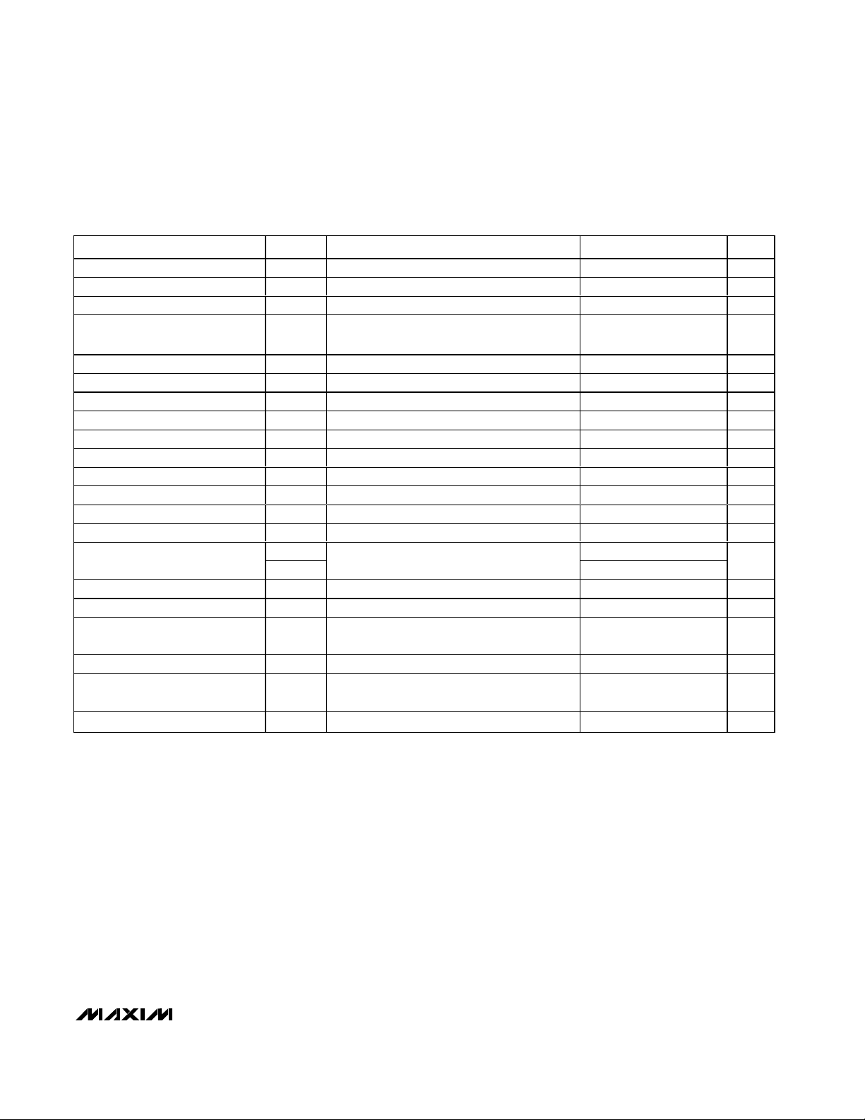
16
15
14
13
12
11
10
9
1
2
3
4
5
6
7
8
N.C. N.C.
OUT
OUT
OUT
OUT
SET
GND
N.C.
TOP VIEW
MAX8869
TSSOP-EP
IN
IN
RST
IN
IN
SHDN
SS
Pin Configuration
IN
IN
IN
IN
SHDN
SS
OUT
OUT
OUT
OUT
RST
SET
GND
ON
OFF
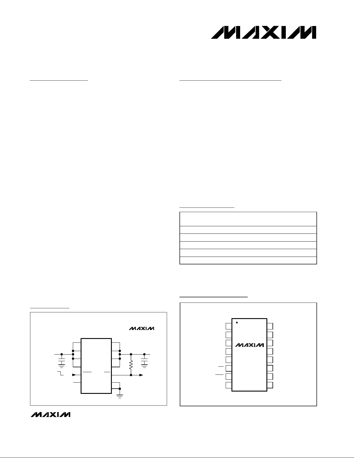
1µF
1µF
IN
+2.7V TO +5.5V
OUT
UP TO 1A
RESET
OUTPUT
MAX8869
Typical Operating Circuit
19-1692; Rev 0; 8/00
For free samples and the latest literature, visit www.maxim-ic.com or phone 1-800-998-8800.
For small orders, phone 1-800-835-8769.
Ordering Information
MicroCap is a trademark of Maxim Integrated Products.
PART
TEMP.
RANGE
PINPACKAGE
V
OUT
*
(V)
MAX8869EUE50
+5.0
MAX8869EUE33
+3.3
MAX8869EUE25
+2.5
MAX8869EUE18
+1.8
MAX8869EUE10
+1.0
*Or adjustable from +0.8V to +5.0V. Contact factory for other
preset output voltages.
**EP = Exposed pad.
-40°C to +85°C 16 TSSOP-EP**
-40°C to +85°C 16 TSSOP-EP
-40°C to +85°C 16 TSSOP-EP
-40°C to +85°C 16 TSSOP-EP
-40°C to +85°C 16 TSSOP-EP
Page 2
MAX8869
1A, MicroCap, Low-Dropout,
Linear Regulator
2 _______________________________________________________________________________________
ABSOLUTE MAXIMUM RATINGS
ELECTRICAL CHARACTERISTICS
(VIN= +2.7V or V
OUT(NOM)
+ 0.5V (whichever is greater), SHDN = IN, SS = open, SET = GND, C
OUT
= 1µF, TA= 0°C to +85°C,
unless otherwise noted. Typical values are at T
A
= +25°C.)
Stresses beyond those listed under “Absolute Maximum Ratings” may cause permanent damage to the device. These are stress ratings only, and functional
operation of the device at these or any other conditions beyond those indicated in the operational sections of the specifications is not implied. Exposure to
absolute maximum rating conditions for extended periods may affect device reliability.
IN, SHDN, RST, SS to GND ......................................-0.3V to +6V
OUT, SET to GND ........................................-0.3V to (V
IN
+ 0.3V)
Output Short-Circuit Duration ........................................Indefinite
Continuous Power Dissipation (T
A
= +70°C)
16-Pin TSSOP-EP (derate 19mW/°C above +70°C).........1.5W
Operating Temperature Range ...........................-40°C to +85°C
Junction Temperature......................................................+150°C
Storage Temperature Range ...............................-65°C to 150°C
Lead Temperature (soldering, 10s) .................................+300°C
PARAMETER
SYMBOL
CONDITIONS
MIN
TYP
MAX
UNITS
Input Voltage Range V
IN
2.7 5.5 V
Input Undervoltage Lockout Typical hysteresis = 50mV
V
Output Voltage Accuracy I
OUT
= 1mA, TA = +85°C-11%
SET Regulation Voltage
(Adjustable Mode)
I
OUT
= 150mA, TA = +85°C
808 mV
Line Regulation
VIN = V
OUT
+ 0.5V to +5.5V, I
OUT
= 10mA 0.1
%/V
Load Regulation
I
OUT
= 1mA to 1A 0.8 1.5
%/A
Ad j ustab l e O utp ut V ol tag e Range
0.8 5 V
Maximum Output Current I
OUT
Continuous 1
A
RMS
Short-Circuit Current Limit I
LIM
V
OUT
= 0 1.0 1.9 A
In-Regulation Current Limit I
LIM
V
SET
= 0.76V 2.0 4.0 A
SET Dual Mode Threshold 40 80 120 mV
SET Input Bias Current I
SET
V
SET
= +0.9V 50 300 nA
I
OUT
= 100µA 0.5 2.0
Ground Current I
GND
I
OUT
= 1A 2.5
mA
I
OUT
= 1mA, +2.7V < VIN < +5.5V 0.2
Dropout Voltage
(Note 1)
I
OUT
= 1A, V
OUT
= +3.3V (Note 2)
350
mV
Output Voltage Noise f = 10Hz to 1M Hz, C
OU T
= 1µF, I
OU T
= 150mA
µV
RMS
Power-Supply Rejection Ratio
f = 100kHz, C
OUT
= 1µF54dB
Shutdown Supply Current I
OFF
SHDN = GND, VIN = +5.5V, V
OUT
= 0 0.1 10 µA
V
IH
1.6
SHDN Input Threshold
V
IL
+2.7V < V
IN
< +5.5V
0.6
V
SHDN Input Bias Current SHDN = GND or IN 0 0.1 µA
Soft-Start Charge Current I
SS
VSS = 0 6 µA
RST Output Low Voltage I
SINK
= 1mA 0.1 V
IN Operating Voltage Range for
RST Valid
I
SINK
= 10µA 1.0 5.5 V
RST Leakage V
RST
= +5.5V
1µA
RST Trip Level Referred to
Nominal V
OUT
Falling edge, typical hysteresis = 10mV 89 92 95
% OUT
RST Release Delay Rising edge 1 3 5.5 ms
Thermal Shutdown Threshold
Typical thermal hysteresis = +20°C
o
C
Dual Mode is a trademark of Maxim Integrated Products.
∆V
LNR
∆V
LDR
PSRR
T
SHDN
2.35 2.45 2.55
792 800
200
150
0.01
170
Page 3
MAX8869
1A, MicroCap, Low-Dropout,
Linear Regulator
_______________________________________________________________________________________ 3
ELECTRICAL CHARACTERISTICS
(VIN= +2.7V or V
OUT(NOM)
+ 0.5V (whichever is greater), SHDN = IN, SS = open, SET = GND, C
OUT
= 1µF, TA= -40°C to +85°C,
unless otherwise noted.) (Note 3)
Note 1: Dropout voltage is (V
IN
- V
OUT
) when V
OUT
falls to 100mV below the value of V
OUT
measured when VIN= V
OUT(NOM)
+0.5V.
Since the minimum input voltage is 2.7V, this specification is only meaningful when V
OUT
≥ 2.7V.
Note 2: The output voltage is externally set using a resistive voltage-divider from OUT to SET.
Note 3: Specifications to -40°C are guaranteed by design, not production tested.
PARAMETER
SYMBOL
CONDITIONS
MIN
MAX
UNITS
Input Voltage Range V
IN
2.7 5.5 V
Input Undervoltage Lockout Typical hysteresis = 50mV 2.3 2.6 V
Output Voltage Accuracy I
OUT
= 1mA, TA = +85°C-11%
SET Regulation Voltage
(Adjustable Mode)
I
OUT
= 150mA, TA = +85°C
808 mV
Load Regulation
I
OUT
= 1mA to 1A 2.0
%/A
Ad j ustab l e O utp ut V ol tag e Rang e 0.8 5 V
Maximum Output Current I
OUT
Continuous 1
A
RMS
Short-Circuit Current Limit I
LIM
V
OUT
= 0 1.0 A
In-Regulation Current Limit I
LIM
V
SET
= +0.76V 2.0 A
SET Dual Mode Threshold 40 120 mV
SET Input Bias Current I
SET
V
SET
= +0.9V 300 nA
Ground Current I
GND
I
OUT
= 100µA 2.0 mA
Dropout Voltage (Note 1) I
OUT
= 1A, V
OUT
= +3.3V (Note 2) 350 mV
Shutdown Supply Current I
OFF
SHDN = GND, VIN = +5.5V, V
OUT
= 0 10 µA
V
IH
1.7
SHDN Input Threshold
V
IL
+2.7V < V
IN
< +5.5V
0.6
V
SHDN Input Bias Current SHDN = GND or IN 0.1 µA
RST Output Low Voltage I
SINK
= 1mA 0.1 V
IN Operating Voltage Range for
RST Valid
I
SINK
= 10µA 1.0 5.5 V
RST Leakage V
RST
= +5.5V 1 µA
RST Trip Level Referred to
Nominal V
OUT
Falling edge, typical hysteresis = 10mV 88 95
% OUT
RST Release Delay Rising edge 1 6 ms
∆V
LDR
792
Page 4

MAX8869
1A, MicroCap, Low-Dropout,
Linear Regulator
4 _______________________________________________________________________________________
Typical Operating Characteristics
(VIN= +5V, V
OUT
= +2.5V, SHDN = IN, SS = open, C
OUT
= 1µF, TA= +25°C, unless otherwise noted.)
0
-1.0
-0.5
-2.0
-1.5
-2.5
-3.0
0 1.0 1.50.5 2.0 2.5 3.0
OUTPUT VOLTAGE DEVIATION
vs. OUTPUT CURRENT
MAX8869-01
OUTPUT CURRENT (A)
OUTPUT VOLTAGE DEVIATION (%)
VIN = +5V
VIN = +3V
I
OUT
= 250mA
-1.5
-1.0
-0.5
0
0.5
1.0
1.5
-40 -15 10 35 60 85
OUTPUT VOLTAGE DEVIATION
vs. TEMPERATURE
MAX8869-02
TEMPERATURE (°C)
OUTPUT VOLTAGE DEVIATION (%)
0
1.0
0.5
2.0
1.5
3.0
2.5
3.5
023145
GROUND CURRENT
vs. INPUT VOLTAGE
MAX8869-03
INPUT VOLTAGE (V)
GROUND CURRENT (mA)
I
OUT
= 0.5A
I
OUT
= 1A
I
OUT
= 0
0
1.0
0.5
2.0
1.5
3.0
2.5
3.5
0 400200 600 800 1000
GROUND CURRENT
vs. OUTPUT CURRENT
MAX8869-04
OUTPUT CURRENT (mA)
GROUND CURRENT (mA)
VIN = +3V
VIN = +5V
0
0.5
1.5
1.0
2.0
2.5
-40 10-15 35 60 85
GROUND CURRENT
vs. TEMPERATURE
MAX8869-05
TEMPERATURE (°C)
GROUND CURRENT (mA)
I
OUT
= 250mA
I
OUT
= 0
VIN = +3VVIN = +5V
0
100
50
250
200
150
400
350
300
450
0 500250 750 1000 1250 1500
DROPOUT VOLTAGE
vs. OUTPUT CURRENT
MAX8869-06
OUTPUT CURRENT (mA)
DROPOUT VOLTAGE (mV)
V
OUT
= +3.3V
0
100
50
200
150
250
300
2.5 3.53.0 4.0 4.5 5.0
DROPOUT VOLTAGE
vs. INPUT VOLTAGE
MAX8869-07
INPUT VOLTAGE (V)
DROPOUT VOLTAGE (mV)
I
OUT
= 500mA
IN DROPOUT, V
OUT
≅ V
IN
0
20
10
40
30
60
50
0.01 10.1 10 100 1000
PSRR vs. FREQUENCY
MAX8869-08
FREQUENCY (kHz)
PSRR (dB)
I
OUT
= 300mA
10
0.01
0.01
10
1000
OUTPUT NOISE SPECTRAL DENSITY
vs. FREQUENCY
0.1
1
MAX8869-09
FREQUENCY (kHz)
NOISE (
µ
V/
√
Hz)
0.1
1
100
I
OUT
= 250mA
Page 5

MAX8869
1A, MicroCap, Low-Dropout,
Linear Regulator
_______________________________________________________________________________________ 5
0
0.001 10.10.01
OUTPUT NOISE
vs. OUTPUT CURRENT
60
20
140
100
180
80
40
160
120
MAX8869-10
OUTPUT CURRENT (A)
OUTPUT NOISE (µV
RMS
)
200µs/div
LINE-TRANSIENT RESPONSE
MAX8869-11
V
IN
V
OUT
5V
3.6V
10mV/div
AC-COUPLED
I
OUT
= 250mA
20µs/div
LOAD-TRANSIENT RESPONSE
MAX8869-12
I
OUT
V
OUT
1A
100mA
50mV/div
AC-COUPLED
20µs/div
LOAD-TRANSIENT RESPONSE
MAX8869-13
I
OUT
V
OUT
3A
10mA
200mV/div
AC-COUPLED
4ms/div
1MHz BANDWIDTH
OUTPUT NOISE
MAX8869-14
100µV/div
I
OUT
= 100µA
40µs/div
SHUTDOWN RESPONSE
MAX8869-15
5V/div
V
OUT
V
SHDN
2V/div
10ms/div
SOFT-START RESPONSE
MAX8869-16
5V/div
CSS = 100nF
I
IN
2V/div
V
OUT
1A/div
V
SHDN
1ms/div
RESET OUTPUT RESPONSE
MAX8869-17
5V/div
V
IN
V
OUT
2V/div
RST
2V/div
RST
OUTPUT
DELAY
Typical Operating Characteristics (continued)
(VIN= +5V, V
OUT
= +2.5V, SHDN = IN, SS = open, C
OUT
= 1µF, TA= +25°C, unless otherwise noted.)
Page 6

MAX8869
Detailed Description
The MAX8869 features Dual Mode operation, allowing a
fixed output of +5V, +3.3V, +2.5V, +1.8V, or +1.0V, or
adjustable output from +0.8V to +5.0V. The regulators
are guaranteed to supply 1A of continuous output current with only 1µF of output capacitance.
As shown in the functional diagram (Figure 1), the
device has a 0.8V reference, error amplifier, MOSFET
driver, P-channel pass transistor, internal feedback
voltage-divider, soft-start function, reset timer, and Dual
Mode and low V
OUT
comparators.
The 0.8V reference is connected to the error amplifier’s
inverting input. The error amplifier compares this reference with the selected feedback voltage and amplifies
the difference. The MOSFET driver reads the error signal and applies the appropriate drive to the P-channel
transistor. If the feedback voltage is high, the pass transistor’s gate is pulled up, allowing less current to pass
to the output. The low V
OUT
comparator senses when
the feedback voltage has dropped 8% below its
expected level, causing RST to go low.
The output voltage is fed back through either an internal resistor-divider connected to OUT or an external
resistor network connected to SET. The Dual Mode
comparator examines V
SET
and selects the feedback
path. If V
SET
is below 80mV, the internal feedback path
is used and the output voltage is regulated to the factory-preset voltage. Otherwise, the output voltage is set
with the external resistor-divider.
Internal P-Channel Pass Transistor
The MAX8869 features a 1A P-channel MOSFET pass
transistor. Unlike similar designs using PNP pass transistors, P-channel MOSFETs require no base drive,
which reduces quiescent current. PNP-based regulators also waste considerable current in dropout when
the pass transistor saturates and use high base-drive
currents under large loads. The MAX8869 does not suffer from these problems and consumes only 500µA of
quiescent current even in dropout.
1A, MicroCap, Low-Dropout,
Linear Regulator
6 _______________________________________________________________________________________
Pin Description
PIN NAME FUNCTION
1, 9, 16 N.C. No Connection. Not internally connected.
2, 3, 4, 5 IN
Regulator Input. Connect to power source (+2.7V to +5.5V). Bypass with 1µF or greater
capacitor to GND (see Capacitor Selection and Regulator Stability). Connect all IN pins
together for proper operation.
6 RST
Reset O utp ut. O p en- d r ai n outp ut i s l ow w hen V
OU T
i s 8% b el ow i ts nom i nal va l ue. RST r em ai ns
l ow w hi l e the outp ut vol tag e ( V
OUT
) i s b el ow the r eset thr eshol d and for at l east 3m s after V
OUT
r i ses to w i thi n r eg ul ati on. C onnect a 100kΩ p ul l up r esi stor to O U T to ob tai n an outp ut vol tag e.
7 SHDN
Active-Low Shutdown Input. A logic low reduces the supply current to 0.1µA. Connect SHDN
to IN for normal operation. In shutdown, RST is low and the soft-start capacitor discharges.
8SS
Soft-Start Control Pin. Connect a soft-start capacitor from SS to GND (see Soft-Start Capacitor
Selection). Leave SS open to disable soft-start.
10 GND
Ground. This pin and the exposed pad also function as a heatsink. Solder both to a large pad
or to the circuit-board ground plane to maximize power dissipation.
11 SET
Voltage-Setting Input. Connect SET to GND for factory-preset output voltage. Connect SET to
an external resistor-divider for adjustable output operation.
12, 13, 14, 15
OUT
Regulator Output. Bypass with a 1µF or greater low-ESR capacitor to GND (see Capacitor
Selection and Regulator Stability). Connect all OUT pins together for proper operation.
Page 7

Output Voltage Selection
The MAX8869 features Dual Mode operation. Connect
SET to GND (Figure 2) for preset voltage mode (see
Ordering Information). In adjustable mode, set the output between +0.8V to +5.0V through two external resistors connected as a voltage-divider to SET (Figure 3).
The output voltage is set by the following equation:
V
OUT
= V
SET
(1 + R1 / R2)
where V
SET
= +0.8V. To simplify resistor selection:
R1 = R2 (V
OUT
/ V
SET
- 1)
Since the input bias current at SET is nominally 50nA,
large resistance values can be used for R1 and R2 to
minimize power consumption without losing efficiency.
Up to 80kΩ is acceptable for R2.
In preset voltage mode, the impedance between SET
and ground should be less than 10kΩ. Otherwise, spu-
rious conditions could cause the voltage at SET to
exceed the 80mV Dual Mode threshold.
Shutdown
A logic low on SHDN disables the MAX8869. In shutdown, the pass transistor, control circuitry, reference,
and all biases are turned off, reducing supply current to
typically 0.1µA. Connect SHDN to IN for normal operation. In shutdown, RST is low and the soft-start capacitor is discharged.
RST
Comparator
The MAX8869 features a low V
OUT
indicator that
asserts when the output voltage falls out of regulation.
The open-drain RST goes low when OUT falls 8%
MAX8869
1A, MicroCap, Low-Dropout,
Linear Regulator
_______________________________________________________________________________________ 7
Figure 1. Functional Diagram
Figure 2. Typical Operating Circuit with Preset Output Voltage
MOSFET DRIVER
WITH FOLDBACK
CURRENT LIMIT
SHUTDOWN
LOGIC
0.8V
REFERENCE
SS
GND
SHDN
IN
OUT
RST
SET
V
SS
6µA
736mV
THERMAL
SENSOR
OUT
DELAY TIMER
IN
3ms
SHUTDOWN
ERROR AMP
DUAL MODE
COMPARATOR
80mV
92% V
OUT
DETECTOR
V
SS
PMOS
NMOS
R1
R2
MAX8869
MAX8869
IN
OFF
SS
IN
IN
IN
SHDN
SS
C
IN
1µF
ON
C
OUT
OUT
OUT
OUT
RST
SET
GND
C
1µF
OUT
OUTIN
RESET
OUTPUT
Page 8

MAX8869
below its nominal output voltage. RST remains low for
3ms after OUT has returned to its nominal value. A
100kΩ pullup resistor from RST to a suitable logic supply voltage (typically OUT) provides a logic control signal. RST can be used as a power-on-reset signal to a
microcontroller (µC) or can drive an external LED for
indicating a power failure. RST is low during shutdown.
RST remains valid for an input voltage as low as 1V.
Soft-Start
As shown in Figure 4, a capacitor on SS allows a gradual buildup of the MAX8869 output, reducing the initial
in-rush current peaks at startup. When SHDN is driven
low, the soft-start capacitor is discharged. When SHDN
is driven high or power is applied to the device, a constant 6µA current charges the soft-start capacitor. The
resulting linear ramp voltage on SS increases the current-limit comparator threshold, limiting the P-channel
gate drive (see Soft-Start Capacitor Selection). Leave
SS floating to disable the soft-start feature.
Current Limiting
The MAX8869 features a 4A current limit when the output voltage is in regulation. When the output voltage
drops by 8% below its nominal, the current limit folds
back to 1.7A. The output can be shorted to ground for
an indefinite period of time without damaging the
device. Avoid continuous output current of more than
1A to prevent damage.
Both the in-regulation and short-circuit current limits can
be reduced from their nominal values by reducing the
voltage at the soft-start pin (SS) below 1.25V. The current limits scale proportionately with the voltage by I
LIM
= I
LIM_NOM
✕
(V
SS
/ 1.25). Since the SS pin sources a
nominal 6µA current, the current limit can be set by
tying a resistor (RSS) between SS and GND, so that I
LIM
= I
LIM_NOM
✕
(I
SS
✕
RSS/ 1.25) where ISS= 6µA . With
RSSin place, soft-start can still be achieved by placing
a capacitor (CSS) in parallel with RSS. The output current
now ramps up asymptotically to the reduced current
limit rather than the nominal one, increasing the softstart time. The time required for the current limit to reach
90% of its steady-state value is given by tSS= 2.3
RSSCSS.
Thermal Overload Protection
Thermal overload protection limits total power dissipation in the MAX8869. When the junction temperature
exceeds TJ= +170°C, the thermal sensor turns off the
pass transistor, allowing the IC to cool. The thermal sensor turns the pass transistor on once the IC’s junction
temperature drops approximately 20°C. Continuous
short-circuit conditions will consequently result in a
pulsed output.
Thermal overload protection is designed to safeguard
the MAX8869 in the event of fault conditions. For continuous operation, do not exceed the absolute maximum junction temperature rating of TJ= +150°C.
Operating Region and Power Dissipation
Maximum power dissipation of the MAX8869 depends
on the thermal resistance of the case and circuit board,
the temperature difference between the die junction
and ambient air, and the rate of air flow. The power dissipation across the device is P = I
OUT(VIN
- V
OUT
). The
resulting maximum power dissipation is:
P
MAX
= [(T
J(MAX)
- TA) / (θJC+ θCA)]
where (T
J(MAX)
- TA) is the temperature difference
between the maximum allowed die junction (150°C)
and the surrounding air; θJC(junction to case) is the
1A, MicroCap, Low-Dropout,
Linear Regulator
8 _______________________________________________________________________________________
Figure 3. Typical Operating Circuit with Adjustable Output
Voltage
IN
IN
IN
IN
SHDN
SS
GND
OUT
OUT
OUT
OUT
RST
SET
ON
OFF
C
OUT
1µF
C
IN
1µF
OUTIN
RESET
OUTPUT
MAX8869
R1
R2
Figure 4. Typical Operating Circuit with Soft-Start and CurrentLimit Reduction
IN
IN
IN
IN
SHDN
SS
OUT
OUT
OUT
OUT
RST
SET
GND
ON
OFF
C
OUT
1µF
C
IN
1µF
OUTIN
RESET
OUTPUT
MAX8869
C
SS
R
SS
Page 9

thermal resistance of the package chosen, and θCAis
the thermal resistance from the case through the PC
board, copper traces, and other materials to the surrounding air. Figure 5 shows the allowable power dissipation for typical PC boards at +25°C, +50°C, and
+70°C ambient temperatures.
The MAX8869 TSSOP-EP package features an
exposed thermal pad on its underside. This pad lowers
the package’s thermal resistance by providing a direct
thermal heat path from the die to the PC board.
Additionally, the ground pin (GND) also channels heat.
Connect the exposed thermal pad and GND to circuit
ground by using a large pad (1in2minimum recommended) or multiple vias to the ground plane.
Applications Information
Capacitor Selection and
Regulator Stability
Capacitors are required at the MAX8869 input and output. Connect 1µF or greater capacitors between IN and
GND (CIN) and OUT and GND (C
OUT
). Due to the
MAX8869’s relatively high bandwidth, use only surfacemount ceramic capacitors that have low equivalent
series resistance (ESR) and high self-resonant frequency (SRF). Make the input and output traces at least
2.5mm wide (the width of the four parallel pins), and
connect CINand C
OUT
within 6mm of the IC to minimize the impact of PC board trace inductance. The
width of the ground trace should be maximized underneath the IC to ensure a good connection between pin
10 (GND) and the ground side of the capacitors.
The output capacitor’s ESR and SRF can affect stability
and output noise. Use capacitors with greater than 5MHz
SRF and ESR of 60mΩ or less to ensure stability and
optimum transient response. This is particularly true in
applications with very low output voltage (<2V) and high
output current (>0.5A).
Since some capacitor dielectrics may vary over bias
voltage and temperature, consult the capacitor manufacturer specifications to ensure that the capacitors
meet these requirements over all voltage and temperature conditions used.
Soft-Start Capacitor Selection
A capacitor (CSS) connected from SS to GND causes
the MAX8869 output current to slowly rise during startup, reducing stress on the input supply. The rise time to
full current limit (tSS) is determined by:
tSS= 2.08 ✕10
-4
✕
C
SS
where CSSis in nF. Typical capacitor values between
10nF to 100nF, with a 5V rating, are sufficient.
Because this ramp is applied to the current-limit comparator, the actual time for the output voltage to ramp
up depends on the load current and output capacitor.
Leave SS open to disable soft-start.
Input-Output (Dropout) Voltage
A regulator’s minimum input-to-output voltage differential (dropout voltage) determines the lowest usable supply voltage. In battery-powered systems, this
determines the useful end-of-life battery voltage. Since
a 0.2Ω P-channel MOSFET is used as the pass device,
dropout voltage is the product of R
DS(ON
) and load
current (see Electrical Characteristics and Dropout
Voltage vs. Output Current in Typical Operating
Characteristics). The MAX8869 operating current
remains low in dropout.
Noise, PSRR, and Transient Response
The MAX8869 is designed to achieve low dropout voltage and low quiescent current in battery-powered systems while still maintaining good noise, transient
response, and AC rejection (see PSRR vs. Frequency
in the Typical Operating Characteristics). When operating from very noisy sources, supply noise rejection and
transient response can be improved by increasing the
values of the input and output capacitors and employing passive postfiltering. MAX8869 output noise is typically 150µV
RMS.
(see the Output Noise plot in the
Typical Operating Characteristics).
MAX8869
1A, MicroCap, Low-Dropout,
Linear Regulator
_______________________________________________________________________________________ 9
Figure 5. Power Operating Region: Maximum Output Current
vs. Input-Output Differential Voltage
0
0.6
0.4
0.2
0.8
1.0
1.2
103245
INPUT-OUTPUT DIFFERENTIAL VOLTAGE
MAXIMUM OUTPUT CURRENT (A)
MAXIMUM CONTINUOUS CURRENT
TYPICAL SUPPLY VOLTAGE LIMIT
TA = +70°C
TA = +50°C
TA = +25°C
TJ = +150°C
TYPICAL DROPOUT
VOLTAGE LIMIT
Chip Information
TRANSISTOR COUNT: 1088
Page 10

MAX8869
1A, MicroCap, Low-Dropout,
Linear Regulator
Package Information
TSSOP.EPS
Note: The MAX8869EUE has an exposed thermal pad on the bottom side of the package.
Maxim cannot assume responsibility for use of any circuitry other than circuitry entirely embodied in a Maxim product. No circuit patent licenses are
implied. Maxim reserves the right to change the circuitry and specifications without notice at any time.
10 ____________________Maxim Integrated Products, 120 San Gabriel Drive, Sunnyvale, CA 94086 408-737-7600
© 2000 Maxim Integrated Products Printed USA is a registered trademark of Maxim Integrated Products.
 Loading...