Maxim MAX8867EUK29-T, MAX8867EUK30-T, MAX8867C-D50, MAX8867C-D29, MAX8867C-D30 Datasheet
...
For free samples & the latest literature: http://www.maxim-ic.com, or phone 1-800-998-8800.
For small orders, phone 408-737-7600 ext. 3468.
_______________General Description
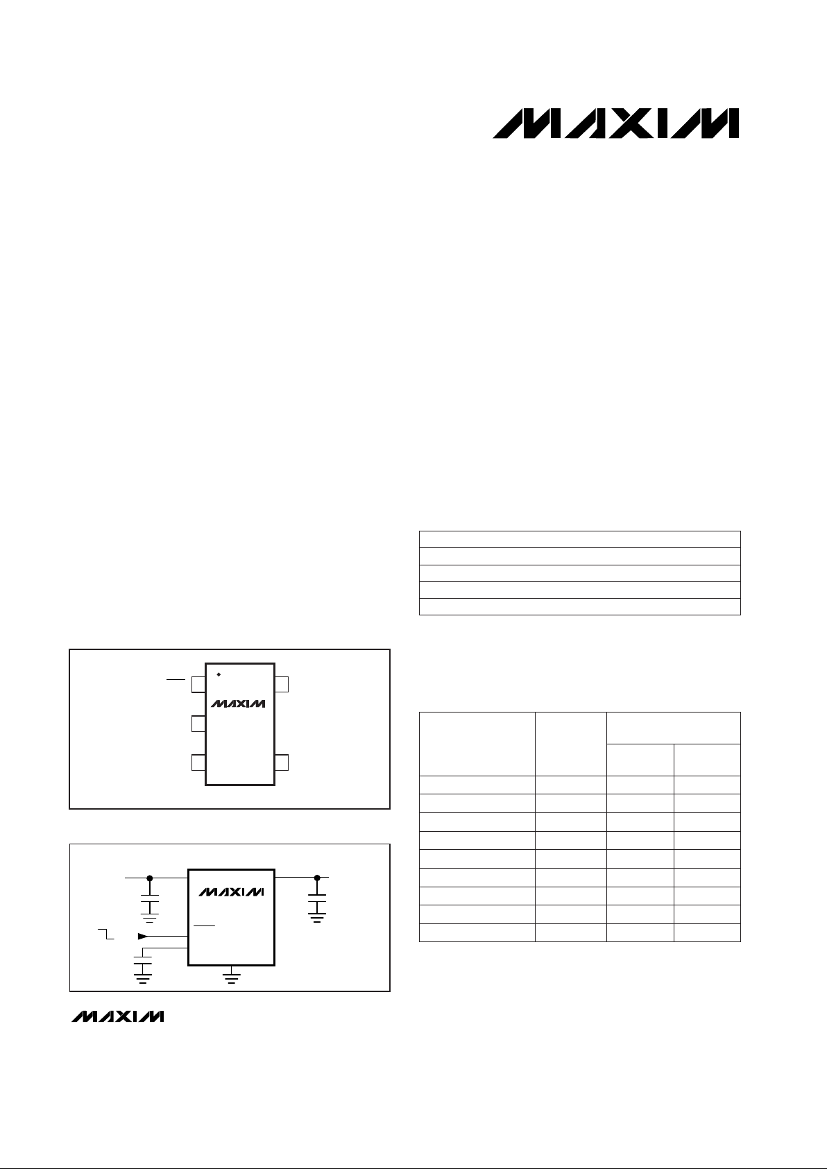
The MAX8867/MAX8868 low-noise, low-dropout linear
regulators operate from a 2.5V to 6.5V input and deliver
up to 150mA. Typical output noise for these devices is
just 30µV
RMS
, and typical dropout is only 165mV at
150mA. The output voltage is preset to voltages in the
range of 2.5V to 5.0V, in 100mV increments. The
MAX8867 and MAX8868 are pin-compatible with the
MAX8863 and MAX8864, except for the BP pin.
Designed with an internal P-channel MOSFET pass
transistor, the MAX8867/MAX8868 maintain a low
100µA supply current, independent of the load current
and dropout voltage. Other features include a 10nA
logic-controlled shutdown mode, short-circuit and thermal-shutdown protection, and reverse battery protection. The MAX8868 also includes an auto-discharge
function, which actively discharges the output voltage
to ground when the device is placed in shutdown. Both
devices come in a miniature 5-pin SOT23 package.
________________________Applications
Cellular Telephones Modems
Cordless Telephones Hand-Held Instruments
PCS Telephones Palmtop Computers
PCMCIA Cards Electronic Planners
____________________________Features
♦ Low Output Noise: 30µV
RMS
♦ Low 55mV Dropout at 50mA Output
(165mV at 150mA output)
♦ Low 85µA No-Load Supply Current
♦ Low 100µA Operating Supply Current
(even in dropout)
♦ Thermal-Overload and Short-Circuit Protection
♦ Reverse Battery Protection
♦ Output Current Limit
♦ Preset Output Voltages (±1.4% accuracy)
♦ 10nA Logic-Controlled Shutdown
MAX8867/MAX8868
Low-Noise, Low-Dropout,
150mA Linear Regulators in SOT23
________________________________________________________________
Maxim Integrated Products
1
GND
OUTIN
15BPSHDN
MAX8867
MAX8868
SOT23-5
TOP VIEW
2
34
__________________Pin Configuration
19-1302; Rev 1; 3/98
PART**
MAX8867C/Dxy
MAX8867EUKxy-T
MAX8868C/Dxy
0°C to +70°C
-40°C to +85°C
0°C to +70°C
TEMP. RANGE PIN-PACKAGE
Dice*
5 SOT23-5
Dice*
______________Ordering Information
___Expanded Ordering Information
*
Dice are tested at TA= +25°C.
**
xy is the output voltage code (see Expanded Ordering
Information table).
***
Other xy between 2.5V and 5.0V are available in 100mV incre-
ments. Contact factory for other versions. Minimum order
quantity is 25,000 units.
MAX8868EUKxy-T -40°C to +85°C 5 SOT23-5
PRESET
OUTPUT
VOLTAGE
(V)
MAX886_EUK25 2.50
OUTPUT
VOLTAGE (xy)
CODE
ACAY
SOT TOP MARK
ACBF
MAX8867 MAX8868
MAX886_EUK28 2.80 ACAZ ACBG
MAX886_EUK29 2.84 ACBA ACBH
MAX886_EUK30 3.00 ACBB ACBI
MAX886_EUK32 3.15 ACBC ACBJ
MAX886_EUK33 3.30 ACBD ACBK
MAX886_EUK36 3.60 ACCZ ACDA
Other xy*** x.y0 — —
MAX886_EUK50 5.00 ACBE ACBL
MAX8867
MAX8868
INPUT
2.5V TO 6.5V
IN OUT
SHDN
C
BP
0.01µF
C
OUT
1µF
C
IN
1µF
OFF
ON
BP
GND
OUTPUT
PRESET
2.5V TO 5.0V
150mA
__________Typical Operating Circuit

MAX8867/MAX8868
Low-Noise, Low-Dropout,
150mA Linear Regulators in SOT23
2 _______________________________________________________________________________________
ABSOLUTE MAXIMUM RATINGS
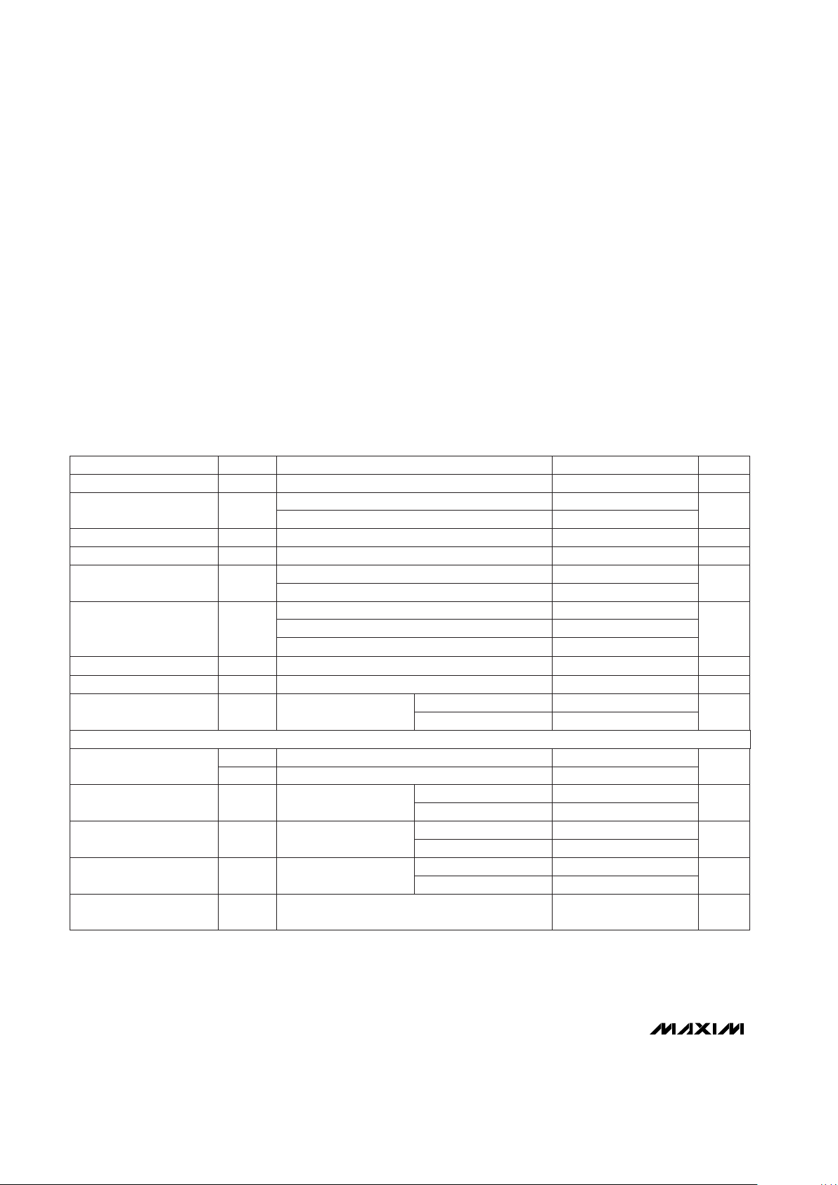
ELECTRICAL CHARACTERISTICS
(VIN= V
OUT(NOMINAL)
+ 0.5V, TA= -40°C to +85°C, unless otherwise noted. Typical values are at TA= +25°C.) (Note 1)
Stresses beyond those listed under “Absolute Maximum Ratings” may cause permanent damage to the device. These are stress ratings only, and functional
operation of the device at these or any other conditions beyond those indicated in the operational sections of the specifications is not implied. Exposure to
absolute maximum rating conditions for extended periods may affect device reliability.
IN to GND....................................................................-7V to +7V
Output Short-Circuit Duration ............................................Infinite
SHDN to GND..............................................................-7V to +7V
SHDN to IN...............................................................-7V to +0.3V
OUT, BP to GND..........................................-0.3V to (V
IN
+ 0.3V)
Continuous Power Dissipation (T
A
= +70°C)
SOT23-5 (derate 7.1mW/°C above +70°C)...................571mW
Operating Temperature Range ...........................-40°C to +85°C
Junction Temperature......................................................+150°C
θ
JB
..................................................................................140°C/W
Storage Temperature Range.............................-65°C to +160°C
Lead Temperature (soldering, 10sec).............................+300°C
C
OUT
= 10µF
C
OUT
= 100µF
VIN= 2.5V to 5.5V
I
OUT
= 0mA, TA= +25°C
2.0
f = 10Hz to 100kHz,
C
BP
= 0.01µF
TA= +25°C 0.01 1
TA= +85°C
I
OUT
= 0mA to 120mA, C
OUT
= 1µF
No load
I
OUT
= 150mA
V
OUT
= 0V
I
OUT
= 150mA
VIN= 2.5V to 5.5V
CONDITIONS
TA= +25°C
µA
V
0.01 100
V
IH
0.4
SHDN Input Threshold
I
Q, SHDN
0.2
Shutdown Supply Current
TA= +25°C
TA= +85°C
V
SHDN
= V
IN
nAI
SHDN
0.5
SHDN Input Bias Current
V
IL
300MAX8868 only
Shutdown Discharge
Resistance
Ω
mA150Maximum Output Current
-1.4 1.4
V2.5 6.5V
IN
Input Voltage (Note 2)
µV
RMS
20
e
n
30
Output Voltage Noise
%/mA0.01 0.04∆V
LDR
Load Regulation
mA160 390I
LIM
Current Limit
I
OUT
= 1mA
85 180
I
OUT
= 50mA
Ground Pin Current µA
100
I
Q
1.1
165
UNITSMIN TYP MAXSYMBOLPARAMETER
Dropout Voltage (Note 2) mV
55 120
30 150
TA= -40°C to +85°C
CBP= 0.1µF,
C
OUT
= 1µF, no load
µs
300
Shutdown Exit Delay
(Note 3)
VIN= (V
OUT
+ 0.1V) to 6.5V, I
OUT
= 1mA %/V-0.15 0 0.15∆V
LNR
Line Regulation
I
OUT
= 0mA to 120mA
%
-3 2
Output Voltage Accuracy
SHUTDOWN

MAX8867/MAX8868
Low-Noise, Low-Dropout,
150mA Linear Regulators in SOT23
_______________________________________________________________________________________ 3
ELECTRICAL CHARACTERISTICS (continued)
(VIN= V
OUT(NOMINAL)
+ 0.5V, TA= -40°C to +85°C, unless otherwise noted. Typical values are at TA= +25°C.) (Note 1)
Note 1: Limits are 100% production tested at T
A
= +25°C. Limits over the operating temperature range are guaranteed through
correlation using Statistical Quality Control (SQC) Methods.
Note 2: The dropout voltage is defined as V
IN
- V
OUT
, when V
OUT
is 100mV below the value of V
OUT
for VIN= V
OUT
+ 0.5V.
Note 3: Time needed for V
OUT
to reach 95% of final value.
CONDITIONS
°C155T
SHDN
Thermal Shutdown
Temperature
UNITSMIN TYP MAXSYMBOLPARAMETER
°C15∆T
SHDN
Thermal Shutdown
Hysteresis
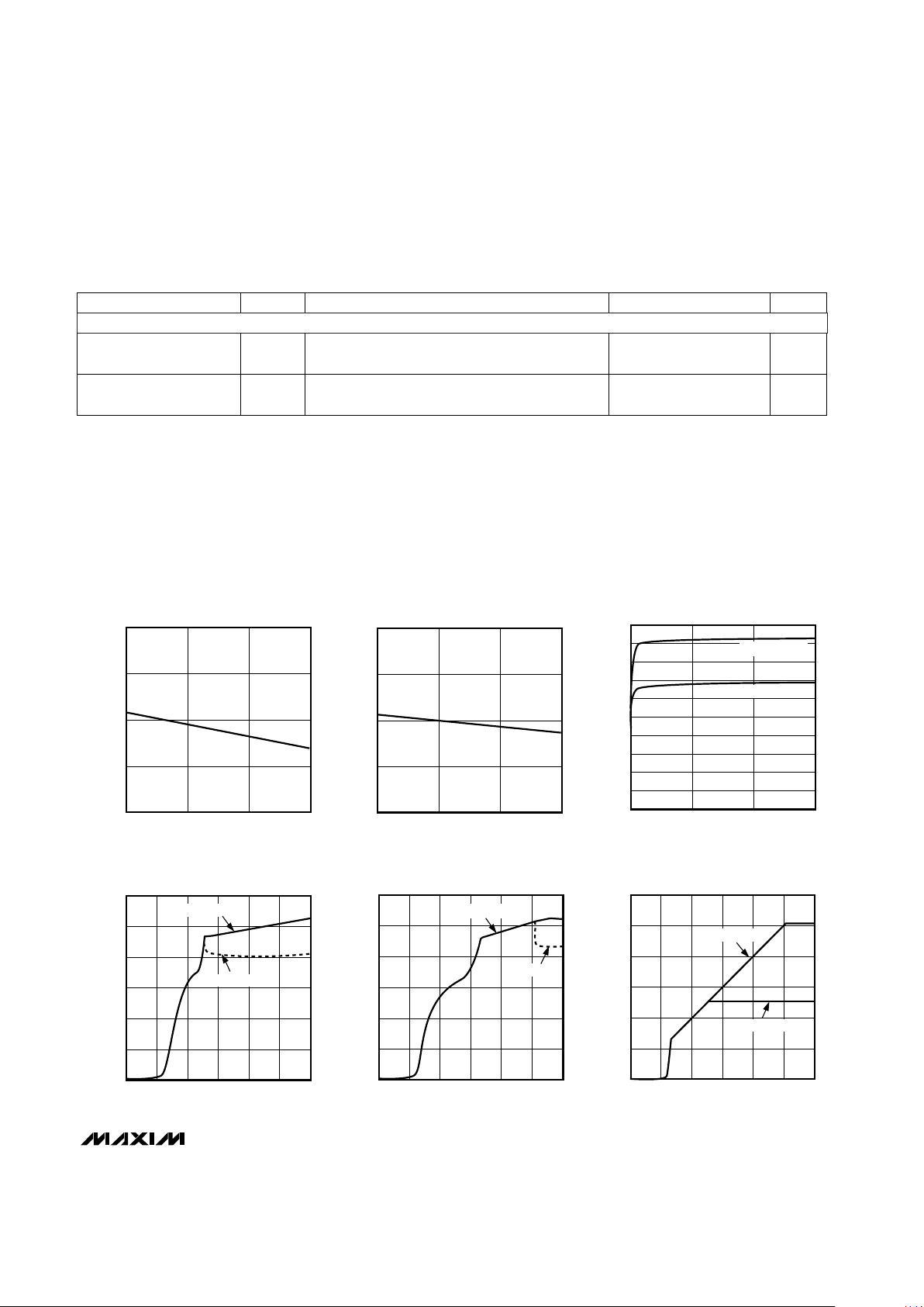
__________________________________________Typical Operating Characteristics
(VIN= V
OUT(NOMINAL)
+ 0.5V, CIN= 1µF, C
OUT
= 1µF, CBP= 0.01µF, TA= +25°C, unless otherwise noted.)
2.40
2.45
2.50
2.55
2.60
0 50 100 150
MAX886_EUK25
OUTPUT VOLTAGE vs. LOAD CURRENT
MAX8867/8-01
LOAD CURRENT (mA)
OUTPUT VOLTAGE (V)
4.8
4.9
5.0
5.1
5.2
0 50 100 150
MAX886_EUK50
OUTPUT VOLTAGE vs. LOAD CURRENT
MAX8867/8-02
LOAD CURRENT (mA)
OUTPUT VOLTAGE (V)
60
70
65
85
80
75
100
95
90
110
105
0 50 100 150
GROUND PIN CURRENT
vs. LOAD CURRENT
MAX8867/8-03
LOAD CURRENT (mA)
GROUND PIN CURRENT (µA)
MAX886_EUK50
MAX886_EUK25
THERMAL PROTECTION
0
20
60
40
80
100
120
0 21 3 54 6
MAX886_EUK25
GROUND PIN CURRENT vs. INPUT VOLTAGE
MAX8867/8-04
INPUT VOLTAGE (V)
GROUND PIN CURRENT (µA)
I
LOAD
= 50mA
NO LOAD
0
20
60
40
80
100
120
0 21 3 54 6
MAX886_EUK50
GROUND PIN CURRENT vs. INPUT VOLTAGE
MAX8867/8-05
INPUT VOLTAGE (V)
GROUND PIN CURRENT (µA)
I
LOAD
= 50mA
NO LOAD
0
1
3
2
4
5
6
0 21 3 54 6
OUTPUT VOLTAGE vs. INPUT VOLTAGE
MAX8867/8-06
INPUT VOLTAGE (V)
OUTPUT VOLTAGE (V)
MAX886_EUK50
MAX886_EUK25
 Loading...