

Datasheet MAX8860EUA28, MAX8860EUA27, MAX8860EUA25, MAX8860EUA18, MAX8860EUA30 Datasheet (Maxim)
...
For free samples & the latest literature: http://www.maxim-ic.com, or phone 1-800-998-8800.
For small orders, phone 1-800-835-8769.
General Description
The MAX8860 low-noise, low-dropout linear regulator
operates from a +2.5V to +6.5V input and is guaranteed to deliver 300mA. Typical output noise for this
device is 60µV
RMS
, and typical dropout is 105mV at
200mA. In addition to the six available preset output
voltages (+1.8V, +2.5V, +2.77V, +2.82V, +3.0V, and
+3.3V), the Dual Mode™ feature allows the device to
be configured as an adjustable output regulator from
+1.25V to +6.5V.
Designed with an internal P-channel MOSFET pass transistor, the MAX8860 has a low 120µA supply current. An
output fault-detection circuit indicates loss of regulation.
Other features include a 10nA, logic-controlled shutdown mode, short-circuit and thermal-shutdown protection, and reverse battery protection. The MAX8860 is
available in a miniature 8-pin µMAX package.
Applications
Wireless Handsets
DSP Core Power
PCMCIA Cards
Hand-Held Instruments
Palmtop Computers
Electronic Planners
Features
♦ High Output Current (300mA)
♦ Low Output Voltage Noise: 60µV
RMS
♦ Low 105mV Dropout at 200mA Output
♦ Low 120µA No-Load Supply Current
♦ Thermal-Overload and Short-Circuit Protection
♦ Reverse Battery Protection
♦ 10nA Logic-Controlled Shutdown
♦ FAULT
Indicator
♦ Small, Space-Saving µMAX Package
(1.1mm max height)
♦ Small 2.2µF Output Capacitor
Saves Space and Cost
MAX8860
Low-Dropout, 300mA
Linear Regulator in µMAX
________________________________________________________________ Maxim Integrated Products 1
1
2
3
4
8
7
6
5
FAULT
SHDN
CC
SETOUT
GND
IN
OUT
MAX8860
µMAX
TOP VIEW
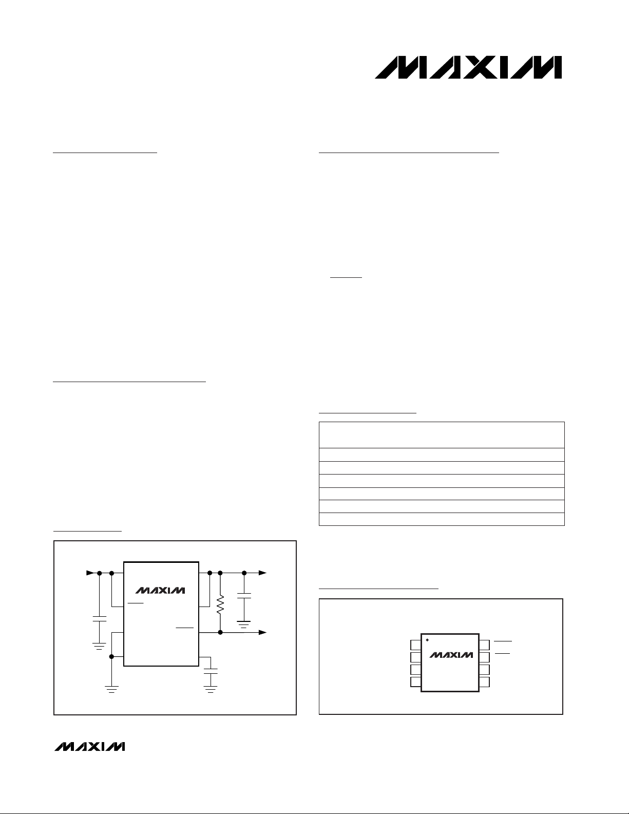
Typical Operating Circuit
19-1422; Rev 1; 12/99
MAX8860EUA18
MAX8860EUA28 -40°C to +85°C
-40°C to +85°C 8 µMAX
8 µMAX
Pin Configuration
Ordering Information
Dual Mode is a trademark of Maxim Integrated Products.
MAX8860EUA33 -40°C to +85°C 8 µMAX
PART TEMP. RANGE
PIN-
PACKAGE
+1.80
+2.82
+3.30
V
OUT
(V)
+2.77MAX8860EUA27 -40°C to +85°C 8 µMAX
+2.50MAX8860EUA25 -40°C to +85°C 8 µMAX
MAX8860EUA30 -40°C to +85°C +3.008 µMAX
C2
2.2µF
OUTPUT
UP TO
300mA
FAULTDETECT
OUTPUT
INPUT
+2.5V TO
+6.5V
C1
2.2µF
IN
MAX8860
SHDN
SET
GND
OUT
OUT
FAULT
CC
R1
100k
C3
33nF
MAX8860
Low-Dropout, 300mA
Linear Regulator in µMAX
2 _______________________________________________________________________________________
ABSOLUTE MAXIMUM RATINGS
ELECTRICAL CHARACTERISTICS
(VIN= +3.6V, CCC= 33nF, TA= -40°C to +85°C, unless otherwise noted. Typical values are at TA= +25°C.) (Note 1)
Stresses beyond those listed under “Absolute Maximum Ratings” may cause permanent damage to the device. These are stress ratings only, and functional
operation of the device at these or any other conditions beyond those indicated in the operational sections of the specifications is not implied. Exposure to
absolute maximum rating conditions for extended periods may affect device reliability.
IN, SHDN to GND .......................................................-7V to +7V
SHDN to IN ...............................................................-7V to +0.3V
SET, CC, FAULT to GND ..........................................-0.3V to +7V
OUT to GND .............................................. -0.3V to (V
IN
+ 0.3V)
FAULT Sink Current ...........................................................20mA
Continuous Output Current ..............................................330mA
Output Short-Circuit Duration ....................................Continuous
Continuous Power Dissipation (T
A
= +70°C)
8-Pin µMAX (derate 4.1mW/°C above +70°C) ............330mW
Thermal Resistance (θ
JA
)
8-Pin µMAX ............................................................+244°C/W
Operating Temperature Range
MAX8860EUA_ _ ...........................................-40°C to +85°C
Junction Temperature......................................................+150°C
Storage Temperature Range ............................-65°C to +150°C
Lead Temperature (soldering, 10sec) ............................+300°C
I
OUT
= 100µA to 300mA
VIN= +2.5V to +6.5V, SET = OUT, I
OUT
= 1mA
I
OUT
= 300mA
I
OUT
= 200mA
I
OUT
= 1mA
DC average current rating
V
OUT
= 0, SHDN = GND
SET = GND
CONDITIONS
%/mA
0.0006
Load Regulation
0.0001
%/V-0.1 0.01 0.1Line Regulation
mV
155
Dropout Voltage (Note 4) 105 220
0.6
µA
0.05
Shutdown Supply Current
0.01 1
µA
165
Supply Current
120 270
3.24 3.3 3.35
V2.5 6.5Input Voltage (Note 2)
mA330 770Output Current Limit
mA300Maximum Output Current
1.230 1.248 1.267
UNITSMIN TYP MAXPARAMETER
V1.25 6.5
Adjustable Output Voltage
Range (Note 3)
TA= +25°C
MAX8860EUA33
TA= -40°C to +85°C 3.21 3.38
TA= +25°C
MAX8860EUA30
TA= -40°C to +85°C 2.92 3.08
2.95 3.00 3.05
TA= +25°C
MAX8860EUA28
TA= -40°C to +85°C 2.75 2.90
2.78 2.82 2.87
I
OUT
= 0
I
OUT
= 300mA
TA= +25°C
TA= +85°C
SET = OUT
SET = GND
SET Threshold Voltage V
SET = OUT, VIN= +2.5V to +6.5V,
I
OUT
= 1mA
1.220 1.275
TA= +25°C
TA= -40°C to +85°C
100µA < I
OUT
< 300mA,
VIN= V
OUT
+1V,
SET = GND
TA= +25°C
MAX8860EUA25
TA= +25°C
MAX8860EUA27
TA= -40°C to +85°C
TA= -40°C to +85°C
2.70 2.84
2.43 2.57
2.73 2.77 2.81
2.46 2.50 2.54
TA= +25°C
VOutput Voltage
MAX8860EUA18
TA= -40°C to +85°C 1.755 1.845
1.77 1.80 1.83
MAX8860
Low-Dropout, 300mA
Linear Regulator in µMAX
_______________________________________________________________________________________ 3
ELECTRICAL CHARACTERISTICS (continued)
(VIN= +3.6V, CCC= 33nF, TA= -40°C to +85°C, unless otherwise noted. Typical values are at TA= +25°C.) (Note 1)
Note 1: Specifications to -40°C are guaranteed by design and not production tested.
Note 2: Guaranteed by line-regulation test.
Note 3: Adjustable mode only.
Note 4: The dropout voltage is defined as V
IN
- V
OUT
when V
OUT
is 100mV below the value of V
OUT
for VIN= V
OUT
+2V. Since the
minimum input voltage is 2.5V, this is applicable only for voltages of 2.5V or higher.
Note 5: The FAULT detection voltage is the difference from input to output voltage. Maintain the input above this level to ensure
good line and load regulation.
C
OUT
= 10µF, V
OUT
to 90% of final value
VIN= +2.5V, I
SINK
= 2mA
SHDN = GND or IN
V
SET
= +1.3V
CONDITIONS
µs120Start-Up Time
°C20Thermal Shutdown Hysteresis
°C170Thermal Shutdown Temperature
nA
0.01 100
0.01 100
V0.25
FAULT Output Low Voltage
nA
0.5
SHDN Input Bias Current
0.01 2.5
nA
0.5
SET Input Leakage Current (Note 3)
UNITSMIN TYP MAXPARAMETER
TA= +25°C
TA= +85°C
60
65
TA= +25°C
TA= +85°C
SET = GND, I
OUT
= 200mA mV130 280
FAULT Detection Voltage (Note 5)
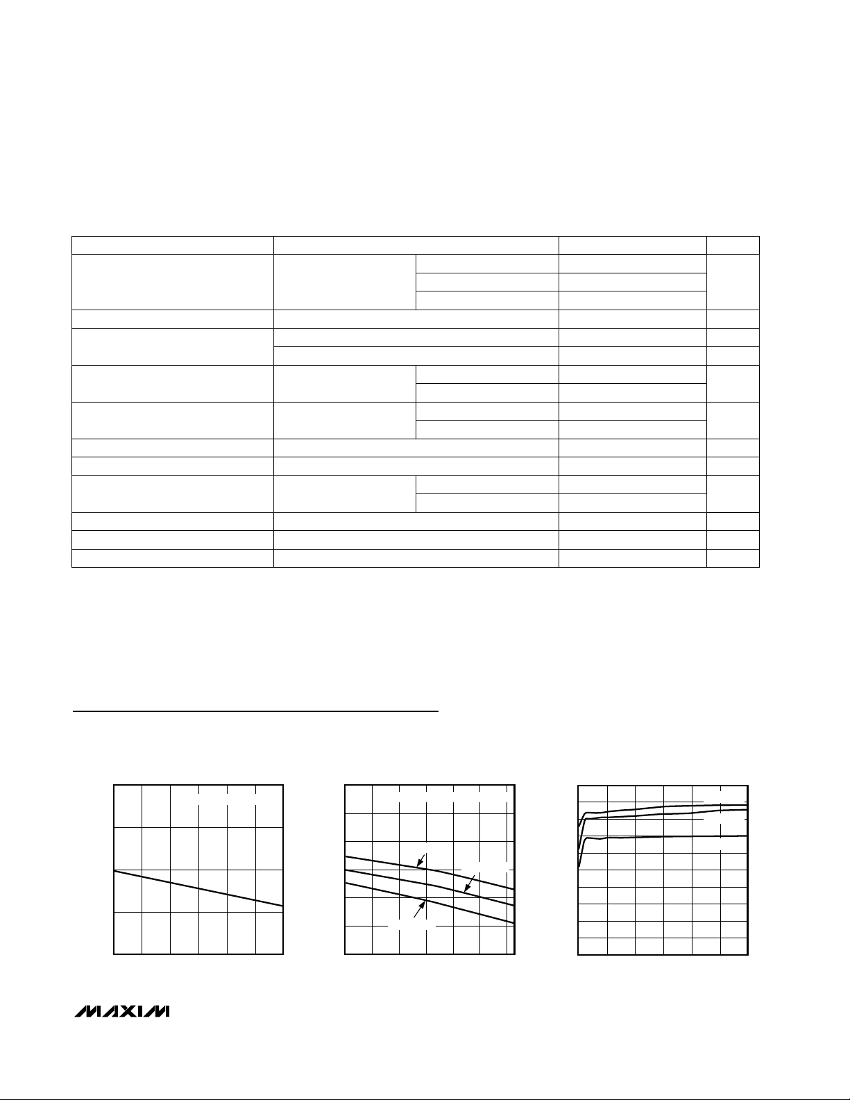
Typical Operating Characteristics
(VIN= V
OUT
+ 0.5V, CIN= C
OUT
= 2.2µF, CCC= 33nF, TA= +25°C, unless otherwise noted.)
-0.4
-0.2
0
0.2
0.4
NORMALIZED OUTPUT VOLTAGE
vs. LOAD CURRENT
MAX8860 toc01
LOAD CURRENT (mA)
OUTPUT VOLTAGE (%)
0 150 20050 100 250 300
V
OUT
NORMALIZED AT I
OUT
= 0
-0.3
-0.1
-0.2
0
0.2
0.1
0.3
NORMALIZED OUTPUT VOLTAGE
vs. TEMPERATURE
MAX8860 toc02
TEMPERATURE (°C)
OUTPUT VOLTAGE (%)
-40 20 40-20 0 60 80
I
OUT
= 0
I
OUT
= 100mA
I
OUT
= 200mA
V
OUT
NORMALIZED AT +25°C, I
OUT
= 0
0
40
120
100
80
60
20
160
140
200
180
0 10050 150 200 250 300
SUPPLY CURRENT vs. LOAD CURRENT
MAX8860 toc03
LOAD CURRENT (mA)
SUPPLY CURRENT (µA)
TA = +85°C
TA = +25°C
TA = -40°C
V
FAULT
= +3.6V
0.5
FAULT Output Off-Leakage Current
TA= +25°C
TA= +85°C
VIL, 2.5V ≤ VIN≤ 5.5V
VIH, 2.5V ≤ VIN≤ 5.5V
V0.4
V2.0
SHDN Input Threshold
C
OUT
= 2.2µF
C
OUT
= 10µF
I
OUT
= 10mA,
10Hz < f < 100kHz
C
OUT
= 100µF
10Hz < f < 100kHz, C
OUT
= 10µF
µV
RMS
190
55
Output Voltage Noise
nV√Hz
Output Voltage Noise Density

MAX8860
Low-Dropout, 300mA
Linear Regulator in µMAX
4 _______________________________________________________________________________________
Typical Operating Characteristics (continued)
(VIN= V
OUT
+ 0.5V, CIN= C
OUT
= 2.2µF, CCC= 33nF, TA= +25°C, unless otherwise noted.)
0
60
40
20
100
80
180
160
140
120
200
0123456
NO LOAD SUPPLY CURRENT
vs. INPUT VOLTAGE
MAX8860 toc04
INPUT VOLTAGE (V)
SUPPLY CURRENT (µA)
TA = +85°C
TA = +25°C
TA = -40°C
20
60
40
120
100
80
160
0
140
180
0 10050 150 200 250 300
DROPOUT VOLTAGE vs. LOAD CURRENT
MAX8860 toc05
LOAD CURRENT (mA)
DROPOUT VOLTAGE (mV)
TA = +85°C
TA = +25°C
TA = -40°C
0
50
150
100
200
250
0 10050 150 200 250 300
FAULT DETECT THRESHOLD
vs. LOAD CURRENT
MAX8860 toc06
LOAD CURRENT (mA)
FAULT DETECT THRESHOLD (mV)
FAULT = HIGH
FAULT = LOW
-70
-50
-60
-30
-40
-10
-20
0
0.01 10.1 10 100 1000
POWER-SUPPLY REJECTION RATIO
vs. FREQUENCY
MAX8860 toc07
FREQUENCY (kHz)
PSRR (dB)
200mA
I
LOAD
0
LOAD-TRANSIENT RESPONSE
MAX8860 toc10
400µs/div
V
OUT
20mV/div
VIN = V
OUT
+ 200mV
0.1 101 100 1000
OUTPUT NOISE SPECTRAL DENSITY
MAX8860 toc08
FREQUENCY (kHz)
NOISE (µV/√Hz)
0.01
0.1
1.0
10
C
OUT
= 2.2µF
C
OUT
= 10µF
I
LOAD
= 10mA
V
OUT
500µV/div
OUTPUT NOISE
(10Hz TO 1MHz)
MAX8860 toc09
1ms/div
I
LOAD
= 200mA
+4.3V
LINE-TRANSIENT RESPONSE
MAX8860 toc12
500µs/div
V
OUT
2mV/div
V
IN
+3.3V
I
LOAD
= 200mA

MAX8860
Low-Dropout, 300mA
Linear Regulator in µMAX
_______________________________________________________________________________________ 5
Typical Operating Characteristics (continued)
(VIN= V
OUT
+ 0.5V, CIN= C
OUT
= 2.2µF, CCC= 33nF, TA= +25°C, unless otherwise noted.)
NAME
FUNCTION
1, 4 OUT Regulator Output. Bypass with 2.2µF, low-ESR capacitor to GND for stable operation.
PIN
Pin Description
4V
2V
0
4V
3V
2V
1V
0
POWER-UP RESPONSE
MAX8860 toc13
5ms/div
FAULT
V
OUT
V
IN
4V
2V
0
4V
3V
2V
1V
0
POWER-DOWN RESPONSE
MAX8860 toc14
2ms/div
V
OUT
V
IN
FAULT
4V
2V
0
3V
2V
1V
0
SHUTDOWN/POWER-UP
MAX8860 toc15
400µs/div
V
OUT
SHDN
2 IN Supply Input. Connect to power source (+2.5V to +6.5V). Bypass with 2.2µF capacitor to GND.
3 GND Ground
5 SET
Output Voltage Set. Connect to GND for internally set threshold. Connect to resistor-divider for adjustable
output voltages. See Output Voltage Selection section for more information.
6 CC Compensation Capacitor. Connect a 0.033µF capacitor from CC to GND.
7
SHDN Shutdown Input. Connect to IN for normal operation. Drive SHDN low to turn off the regulator.
8
FAULT
Fault Output. A high-impedance, open-drain output. When the MAX8860 is out of regulation, FAULT goes
low. In shutdown, the FAULT pin is high impedance. Connect to GND if unused.
Detailed Description
The MAX8860 is a low-dropout, low-quiescent-current
linear regulator designed primarily for battery-powered
applications. It supplies an adjustable +1.25V to
+6.5V output voltage or a fixed-voltage output of +1.8V
(MAX8860EUA18), +2.5V (MAX8860EUA25), +2.77V
(MAX8860EUA27), +2.82V (MAX8860EUA28), +3.0V
(MAX8860EUA30), or +3.3V (MAX8860EUA33) for load
currents up to 300mA. The devices with 2.77V and
2.82V nominal outputs are designed to guarantee minimum output voltages of 2.70V and 2.75V, respectively.
The device consists of a +1.25V reference, error amplifier, MOSFET driver, P-channel pass transistor, Dual
Mode comparator, fault detector, and internal-feedback
voltage divider (Figure 1).
The 1.25V bandgap reference is connected to the error
amplifier’s inverting input. The error amplifier compares
this reference to the selected feedback voltage and
amplifies the difference. The MOSFET driver reads the
error signal and applies the appropriate drive to the Pchannel pass transistor. If the feedback voltage is lower
than the reference voltage, the pass-transistor gate is
pulled lower, allowing more current to pass and
increasing the output voltage. If the feedback voltage
is higher than the reference voltage, the pass-transistor
gate is driven higher, allowing less current to pass to
the output. The output voltage is fed back through
either an internal resistor voltage divider connected to
OUT, or an external resistor network connected to SET.
The Dual Mode comparator examines V
SET
and selects
the feedback path. If V
SET
is below 60mV, internal
feedback is used and the output voltage is regulated to
the preset output voltage. Additional blocks include an
output current limiter, reverse battery protection, a thermal sensor, a fault detector, and shutdown logic.

MAX8860
Low-Dropout, 300mA
Linear Regulator in µMAX
6 _______________________________________________________________________________________
Internal P-Channel Pass Transistor
The MAX8860 features a 0.5Ω typical P-channel
MOSFET pass transistor. This provides several advantages over similar designs using PNP pass transistors,
including longer battery life. PNP-based regulators
waste considerable amounts of current in dropout when
the pass transistor saturates. They also use high basedrive currents under large loads. The P-channel
MOSFET requires no base-drive current, which reduces
quiescent current considerably. The MAX8860 consumes less than 165µA of quiescent current whether in
dropout, light-load, or heavy-load applications (see
Typical Operating Characteristics).
Output Voltage Selection
The MAX8860 features Dual Mode operation: it operates
in either a preset voltage mode or an adjustable mode.
In preset voltage mode, internal, trimmed feedback
resistors set the output voltage to an adjustable +1.25V
to +6.5V output voltage or a fixed-voltage output of
+1.8V (MAX8860EUA18), +2.5V (MAX8860EUA25),
+2.77V (MAX8860EUA27), +2.82V (MAX8860EUA28),
+3.V (MAX8860EUA30), or +3.3V (MAX8860EUA33).
Select this mode by connecting SET to ground. In
adjustable mode, select an output between 1.25V and
6.5V using two external resistors connected as a voltage
divider to SET (Figure 2). Calculate the output voltage
with the following equation:
where V
SET
= 1.25V. To simplify resistor selection, use
the following equation:
R1 R2
V
V
1
OUT
SET
=−
VV
R
R
OUT SET
=+
1
1
2
SHUTDOWN
LOGIC
ERROR
AMP
1.25V
REF
P
OUT
CC
SET
FAULT
DUAL-MODE
COMPARATOR
60mV
GND
IN
SHDN
MAX8860
THERMAL
SENSOR
FAULT
DETECT
REVERSE
BATTERY
PROTECTION
MOS DRIVER
WITH I
LIMIT
Figure 1. Functional Diagram
Figure 2. Adjustable Output Using External Feedback
Resistors
MAX8860
OUT
SET
FAULT
GND
IN
SHDN
CC
C
OUT
2.2µF
C
IN
2.2µF
33nF
BATTERY
OUTPUT
VOLTAGE
R1
R2
100k

MAX8860
Low-Dropout, 300mA
Linear Regulator in µMAX
_______________________________________________________________________________________ 7
Choose R2 = 100kΩ to optimize power consumption,
accuracy, and high-frequency power-supply rejection.
Ensure that the total current through the external resistive feedback and load resistors is not less than 10µA.
Since the V
SET
tolerance is typically less than ±20mV,
set the output using fixed resistors instead of trim pots.
In preset voltage mode, connect SET to GND. Keep
impedances between SET and ground to less than
100kΩ. Otherwise, spurious conditions can cause V
SET
to exceed the 60mV Dual Mode threshold.
Shutdown
Drive SHDN low to place the MAX8860 in shutdown
mode. In shutdown mode, the pass transistor, control
circuit, reference, and all biases are turned off, reducing the supply current to typically 10nA. Connect SHDN
to IN for normal operation.
Current Limit
The MAX8860 includes short-circuit protection. It includes
a current limiter that controls the pass transistor’s gate
voltage to limit the output current to about 770mA. For
design purposes, the minimum current limit is 330mA.
Thermal-Overload Protection
Thermal-overload protection limits total power dissipation in the MAX8860. When the junction temperature
(TJ) exceeds +170°C, the thermal sensor sends a signal to the shutdown logic, turning off the pass transistor
and allowing the IC to cool. The pass transistor turns on
again after the IC’s junction temperature typically cools
by 20°C, resulting in a pulsed output during continuous
thermal-overload conditions.
Thermal-overload protection is designed to protect the
MAX8860 against fault conditions. Stressing the device
with high-load currents and high input-output differential voltages (which result in die temperatures above
+125°C) may cause a momentary overshoot (2% to 8%
for 200ms) when the load is completely removed.
Remedy this by raising the minimum load current from
0 (+125°C) to 100µA (+150°C). This is accomplished
with an external load resistor. For continuous operation,
do not exceed the absolute maximum junction temperature rating of +150°C.
Operating Region and
Power Dissipation
Maximum power dissipation of the MAX8860 depends
on the thermal resistance of the case and circuit board,
the temperature difference between the die junction
and ambient air, and the rate of air flow. The power dissipated by the device is:
P = I
OUT(VIN
- V
OUT
)
The maximum power dissipation is:
P
MAX
= (T
JMAX
- TA) / θ
JA
where: T
JMAX
= +150°C
TAis the ambient temperature
θJA= 244°C/W
The MAX8860’s pins perform the dual function of providing an electrical connection as well as channeling heat
away from the die. Use wide circuit-board traces and
large, solid copper polygons to improve power dissipation. Using multiple vias to buried ground planes further
enhances thermal conductivity.
Reverse Battery Protection
The MAX8860 has a unique protection scheme that limits the reverse supply current to less than 1mA when
either V
IN
or V
S HDN
falls below GND. The circuitry
monitors the polarity of these two pins, disconnecting
the internal circuitry and parasitic diodes when the
applied voltage is reversed. This feature prevents the
device from overheating and damaging an improperly
installed battery.
Integrator Circuitry
The MAX8860 uses an external 33nF compensation
capacitor for minimizing load- and line-regulation errors
and for lowering output noise. When the output voltage
shifts due to varying load current or input voltage, the
integrator capacitor voltage is raised or lowered to
compensate for the systematic offset at the error amplifier. Compensation is limited to ±5% to minimize transient overshoot when the device goes out of dropout,
current limit, or thermal shutdown.
Fault-Detection Circuitry
When the output voltage goes out of regulation—such
as during dropout, current limit, or thermal shutdown—
FAULT goes low. In addition, the fault-detection circuitry
detects when the input-to-output voltage differential is
insufficient to ensure good load and line regulation at
the output. When the input-to-output voltage differential
is less than 130mV for a load current of 200mA, FAULT
also goes low. The differential threshold is designed to
be always higher than and track with the dropout voltage, and to scale proportionally with load current (see
Fault Detect Threshold vs. Load Current graph in the
Typical Operating Characteristics).
The FAULT pin is an open-drain N-channel MOSFET. To
create a voltage level output, connect a pull-up resistor
from FAULT to OUT. To minimize current consumption,
make this resistor as large as practical. A 100kΩ resistor
works well for most applications.

MAX8860
Low-Dropout, 300mA
Linear Regulator in µMAX
Maxim cannot assume responsibility for use of any circuitry other than circuitry entirely embodied in a Maxim product. No circuit patent licenses are
implied. Maxim reserves the right to change the circuitry and specifications without notice at any time.
8 _____________________Maxim Integrated Products, 120 San Gabriel Drive, Sunnyvale, CA 94086 408-737-7600
© 1999 Maxim Integrated Products Printed USA is a registered trademark of Maxim Integrated Products.
VIN> +5.5V Minimum Load
Current Requirements
When operating the MAX8860 with an input voltage
above +5.5V, a minimum load current of 20µA is
required to maintain regulation in preset voltage mode.
When setting the output with external resistors, ensure
that the minimum current through the external feedback
resistors and load is at least 30µA. This applies only
when the input voltage exceeds +5.5V. For input voltages less than +5.5V, the MAX8860 maintains regulation and stability without external loading.
Applications Information
Capacitor Selection and
Regulator Stability
Typically, use a 2.2µF capacitor on the input and a
2.2µF capacitor on the output of the MAX8860.
Capacitor type is not critical, as long as it has an ESR
less than 0.5Ω. Larger capacitor values and lower ESR
provide better supply-noise rejection and transient
response. Use higher-value capacitors (10µF) if large,
fast input or load transients are anticipated or if the
device is located several inches from the power source.
For stable operation over the full temperature range,
with load currents up to 300mA, a minimum outputcapacitor value of 2.2µF is recommended. There is no
upper limit to capacitor size. The circuit used to generate the typical operating characteristics data used
2.2µF, X7R, 16V (1206) ceramic capacitors. These
capacitors typically have an ESR of 50mΩ.
Power-Supply Rejection and Operation
from Sources Other than Batteries
The MAX8860 is designed to deliver low dropout voltage and low quiescent current in battery-powered systems. Power-supply rejection is 67dB at low frequencies
and rolls off above 100kHz. At high frequencies, the output capacitor is the major contributor to the rejection of
power-supply noise (see the Power-Supply Rejection
Ratio vs. Frequency graph in the Typical Operating
Characteristics).
When operating from sources other than batteries,
improve supply-noise rejection and transient response
by increasing the values of the input and output capacitors, and by using passive filtering techniques (see the
supply and load-transient responses in the Typical
Operating Characteristics).
Load-Transient Considerations
The MAX8860 load-transient response graph (see
Typical Operating Characteristics) shows the output
response due to changing load current. Reduce overshoot by increasing the output capacitor’s value and
decreasing its ESR.
Input-Output (Dropout) Voltage
A regulator’s minimum input-output voltage differential
(or dropout voltage) determines the lowest usable supply
voltage. In battery-powered systems, this determines the
useful end-of-life battery voltage. Because the MAX8860
uses a P-channel MOSFET pass transistor, its dropout
voltage is a function of R
DS(ON)
(typically 0.5Ω) multi-
plied by the load current (see Electrical Characteristics).
Chip Information
TRANSISTOR COUNT: 148
 Loading...