

Page 1
General Description
The MAX882/MAX883/MAX884 linear regulators maxi-
mize battery life by combining ultra-low supply currents
and low dropout voltages. They feature 200mA output
current capability at up to +125°C junction temperature
and come in a 1.5W SOIC package. The 1.5W package
(compared to 0.47W for standard SOIC packages)
allows a wider operating range for the input voltage and
output current. The MAX882/MAX883/MAX884 use a Pchannel MOSFET pass transistor to maintain a low 11µA
(15µA max) supply current from no-load to the full
200mA output. Unlike earlier bipolar regulators, there are
no PNP base current losses that increase with output
current. In dropout, the MOSFET does not suffer from
excessive base currents that occur when PNP transistors
go into saturation. Typical dropout voltages are 220mV
at 5V and 200mA, or 320mV at 3.3V and 200mA.
The MAX882 features a 7µA standby mode that disables
the output but keeps the reference, low-battery comparator, and biasing circuitry alive. The MAX883/MAX884 feature a shutdown (OFF) mode that turns off all circuitry,
reducing supply current to less than 1µA. All three
devices include a low-battery-detection comparator, foldback current limiting, reverse-current protection, and
thermal-overload protection.
The output is preset at 3.3V for the MAX882/MAX884
and 5V for the MAX883. In addition, all devices employ
Dual Mode™ operation, allowing user-adjustable outputs
from 1.25V to 11V using external resistors. The input voltage supply range is 2.7V to 11.5V.
For low-dropout linear regulators with output currents up
to 500mA, refer to the MAX603/MAX604 data sheet.
Applications
Pagers and Cellular Phones
3.3V and 5V Regulators
1.25V to 11V Adjustable Regulators
High-Efficiency Linear Regulators
Battery-Powered Devices
Portable Instruments
Solar-Powered Instruments
Features
♦ Foldback Current Limiting
♦ High-Power (1.5W) 8-Pin SO Package
♦ Dual Mode Operation: Fixed or Adjustable
Output from 1.25V to 11V
♦ Large Input Range (2.7V to 11.5V)
♦ Internal 1.1Ω P-Channel Pass Transistor
Draws No Base Current
♦ Low 220mV Dropout Voltage at 200mA
Output Current
♦ 11µA (typ) Quiescent Current
♦ 1µA (max) Shutdown Mode or 7µA (typ)
Standby Mode
♦ Low-Battery Detection Comparator
♦ Reverse-Current Protection
♦ Thermal-Overload Protection
MAX882/MAX883/MAX884
5V/3.3V or Adjustable, Low-Dropout,
Low IQ, 200mA Linear Regulators
________________________________________________________________ Maxim Integrated Products 1
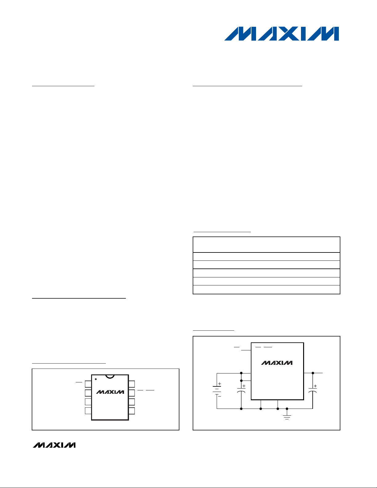
Pin Configuration
Typical Operating Circuit
19-0275; Rev 2; 11/00
Ordering Information continued at end of data sheet.
*Dice are tested at T
J
= +25°C, DC parameters only.
Dual Mode is a trademark of Maxim Integrated Products.
MAX882
MAX883
MAX884
C
IN
O.1µF
C
OUT
2.2µF
OUTPUT
VOLTAGE
INPUT
VOLTAGE
BATTERY
LBI
OFF (STBY)
( ) ARE FOR MAX882.
IN
OUT
GNDSET
ON/OFF
For free samples and the latest literature, visit www.maxim-ic.com or phone 1-800-998-8800.
For small orders, phone 1-800-835-8769.
Ordering Information
PART
TEMP RANGE
PIN-
PACKAGE
PKG
CODE
MAX882CPA 0°C to +70°C 8 PDIP P8-2
MAX882CSA 0°C to +70°C 8 SO S8-6F
MAX882C/D 0°C to +70°C Dice* —
MAX882EPA
8 PDIP P8-2
MAX882ESA
8 SO S8-6F
-40°C to +85°C
-40°C to +85°C
TOP VIEW
1
LBO
2
SET
GND
( ) ARE FOR MAX882.
OUT
MAX882
3
MAX883
MAX884
4
DIP/SO
8
7
6
5
LBI
OFF (STBY)
GND
IN
Page 2
MAX882/MAX883/MAX884
5V/3.3V or Adjustable, Low-Dropout,
Low IQ, 200mA Linear Regulators
2 _______________________________________________________________________________________
ABSOLUTE MAXIMUM RATINGS
ELECTRICAL CHARACTERISTICS
(VIN= 6V (MAX883) or VIN= 4.3V (MAX882/MAX884), C
OUT
= 2.2µF, STBY or OFF = VIN, SET = GND, LBI = VIN, TJ= -40°C to
+85°C, unless otherwise noted. Typical values are at T
J
= +25°C.) (Note 1)
Stresses beyond those listed under “Absolute Maximum Ratings” may cause permanent damage to the device. These are stress ratings only, and functional
operation of the device at these or any other conditions beyond those indicated in the operational sections of the specifications is not implied. Exposure to
absolute maximum rating conditions for extended periods may affect device reliability.
Supply Voltage (IN or OUT to GND).......................-0.3V to +12V
Output Short-Circuit Duration ...............................................1min
Continuous Output Current ...............................................300mA
LBO Output Current............................................................50mA
LBO Output Voltage and LBI,
SET, STBY, OFF Input Voltages ............-0.3V to the greater of
(IN + 0.3V) or (OUT + 0.3V)
Continuous Power Dissipation (T
J
= +70°C)
Plastic DIP (derate 9.09mW/°C above +70°C) ............727mW
High-Power SO (derate 18.75mW/°C above +70°C) .......1.5W
CERDIP (derate 8.00mW/°C above +70°C).................640mW
Operating Temperature Ranges
MAX88_C_A........................................................0°C to +70°C
MAX88_E_A .....................................................-40°C to +85°C
Junction Temperature .....................................................+150°C
Storage Temperature Range .............................-65°C to +160°C
Lead Temperature (soldering, 10s) .................................+300°C
PARAMETER
SYMBOL
CONDITIONS
MIN
TYP
MAX
UNITS
MAX88_C_A 2.7
MAX88_E_A 2.9
Input Voltage Range V
IN
SET = OUT, RL =
1kΩ
MAX88_MJA 3.0
V
0°C ≤ TJ ≤ +85°C
MAX883,
-40°C ≤ TJ ≤ +85°C
0°C ≤ T
J
≤ +85°C
Output Voltage (Note 2) V
OUT
MAX882/MAX884,
-40°C ≤ TJ ≤ +85°C
V
MAX883C_A/E_A 60 100
I
OUT
= 1mA to
200mA
MAX883MJA 150
Load Regulation ∆V
LDR
I
OUT
= 1mA to
150mA
MAX882, MAX884 30 100
mV
Line Regulation ∆V
LNR
10 40 mV
I
OUT
= 100mA
220
MAX883
I
OUT
= 200mA
440
I
OUT
= 100mA
320
Dropout Voltage (Note 3) ∆V
DO
MAX882/MAX884
I
OUT
= 200mA
640
mV
MAX88_C_A/E_A 11 15
SET = OUT, VIN =
6V
MAX88_MJA 30
MAX88_C_A/E_A 15 25
Quiescent Current I
Q
VIN = 11.5V
MAX88_MJA 40
µA
11.5
11.5
11.5
I
= 100µA - 250m A,
OU T
4.75 5.00 5.25
6.0V ≤ VIN ≤ 11.5V
4.3V ≤ VIN ≤ 11.5V
(V
I
= 100µA - 250m A,
OU T
I
= 100µA - 200m A,
OU T
I
= 100µA - 200m A,
OU T
OUT
= 10mA
+ 0.5V) < VIN < 11.5V, I
OUT
4.65 5.35
3.15 3.30 3.45
3.07 3.53
110
220
160
320
Page 3
MAX882/MAX883/MAX884
5V/3.3V or Adjustable, Low-Dropout,
Low IQ, 200mA Linear Regulators
_______________________________________________________________________________________ 3
ELECTRICAL CHARACTERISTICS (continued)
(VIN= 6V (MAX883) or VIN= 4.3V (MAX882/MAX884), C
OUT
= 2.2µF, STBY or OFF = VIN, SET = GND, LBI = VIN, TJ= -40°C to
+85°C, unless otherwise noted. Typical values are at T
J
= +25°C.) (Note 1)
PARAMETER
CONDITIONS
UNITS
MAX882C_A/E_A 7 15
STBY = 0, VIN =
6V, SET = OUT
MAX882MJA 30
MAX882C_A/E_A 10 25
STBY Quiescent Current (Note 4)
I
Q STBY
STBY = 0, VIN =
MAX882MJA 40
µA
MAX88_C_A
1
MAX88_E_A 5
OFF Quiescent Current I
Q OFF
OFF = 0, RL = 1kΩ,
V
IN
= 11.5V
MAX883/MAX884
MAX88_MJA 10
µA
MAX88_C_A 1
MAX88_E_A 3Minimum Load Current
)
VIN = 11.5V, SET =
OUT
MAX88_MJA 10
µA
V
OUT
< 0.8V
Foldback Current Limit (Note 5) ILIM
V
OUT
> 0.8V and VIN - V
OUT
> 0.7V
mA
Thermal Shutdown Temperature
T
SD
°C
Thermal Shutdown Hysteresis ∆T
SD
10 °C
V
OUT
= 4.5V MAX883_A 6 20
Reverse-Current-Protection
(Note 6)
∆V
RTH
V
OUT
= 3.0V
MAX882_A,
MAX884_A
620
mV
MAX882: VIN = 0, STBY = 0, V
OUT
= 3.0V 7
Reverse Leakage Current I
RVL
MAX883/MAX884: VIN = 0, OFF = 0, V
OUT
= 3.0V
µA
Startup Overshoot V
OSH
RL = 1kΩ, C
OUT
= 2.2µF
% of
V
OUT
Time Required to Exit OFF or
STBY Modes
T
START
VIN = 9V, RL = 33Ω, OFF from 0 to VIN, 0%
to 95% of V
OUT
µs
For internal feedback 65 30
Dual Mode SET Threshold
For external feedback
65
mV
0°C ≤ TJ ≤ +85°C
SET Reference Voltage V
SET
SET = OUT, RL =
1kΩ
-40°C ≤ T
J
≤ +85°C
V
SET Input Leakage Current I
SET
V
SET
= 1.5V or 0
nA
0°C ≤ TJ ≤ +85°C
LBI Threshold Voltage V
LBI
LBI signal falling
-40°C ≤ T
J
≤ +85°C
V
LBI Hysteresis ∆V
LBI
7mV
LBI Input Leakage Current I
LBI
V
LBI
= 1.5V
nA
LBO Output Low Voltage V
LBOL
I
LBO
sink = 1.2mA, V
LBI
= 1V, 3V < VIN <
11.5V, SET = OUT
90 250 mV
LBO Output Leakage Current
V
LBI
= VIN, V
LBO
= V
IN
0.1 µA
MAX88_C_A
1
MAX88_E_A 3OUT Leakage Current
VIN = 11.5V, V
OUT
= 2V, SET = OUT
MAX88_MJA 10
µA
SYMBOL
MIN TYP MAX
11.5V, SET = OUT
I
OUT(MIN
V
SET TH
I
BLO LKG
I
OUT LKG
150
1.16 1.20 1.24
1.12 1.28
1.15 1.20 1.25
1.11 1.29
0.01
170
430
+160
0.01
200
±0.01 ±50
±0.01 ±50
0.01
0.01
Page 4
MAX882/MAX883/MAX884
5V/3.3V or Adjustable, Low-Dropout,
Low IQ, 200mA Linear Regulators
4 _______________________________________________________________________________________
Note 1:Electrical specifications are measured by pulse testing and are guaranteed for a junction temperature (TJ) within the operat-
ing temperature range, unless otherwise noted. Specifications to -40°C are guaranteed by design and not production tested.
Note 2:(V
IN
- V
OUT
) is limited to keep the product (I
OUT
x (VIN- V
OUT
)) from exceeding the package power dissipation limits. See
Figure 5. Therefore, the combination of high output current and high supply voltage is not tested.
Note 3:Dropout Voltage is (V
IN
- V
OUT
) when V
OUT
falls to 100mV below its nominal value at VIN= (V
OUT
+ 2V). For example, the
MAX883 is tested by measuring the V
OUT
at VIN= 7V, then VINis lowered until V
OUT
falls 100mV below the measured value.
The difference (VIN- V
OUT
) is then measured and defined as ∆VDO.
Note 4:Since standby mode inhibits the output but keeps all biasing circuitry alive, the Standby Quiescent Current is similar to the
normal operating quiescent current.
Note 5:Foldback Current Limit was characterized by pulse testing to remain below the maximum junction temperature (not
production tested).
Note 6:The Reverse-Current Protection Threshold is the output/input differential voltage (V
OUT
- VIN) at which reverse-current
protection switchover occurs and the pass transistor is turned off. See the section Reverse-Current Protection in the Detailed
Description.
Note 7:Noise is tested using a bandpass amplifier with two poles at 10Hz and two poles at 10kHz.
ELECTRICAL CHARACTERISTICS (continued)
(VIN= 6V (MAX883) or VIN= 4.3V (MAX882/MAX884), C
OUT
= 2.2µF, STBY or OFF = VIN, SET = GND, LBI = VIN, TJ= -40°C to
+85°C, unless otherwise noted. Typical values are at T
J
= +25°C.) (Note 1)
PARAMETER
CONDITIONS
UNITS
STBY Threshold Voltage V
STBY
STBY signal falling, MAX882_A
V
STBY Hysteresis
MAX882_A 7 mV
STBY Input Leakage Current I
STBY
V
STBY
= VIN or 0, MAX882_A
nA
V
IL OFF
In off mode, MAX883_A, MAX884_A 0.4
In on mode, SET = OUT, VIN < 6V,
MAX883_A, MAX884_A
2.0
OFF Threshold Voltage
In on mode, SET = OUT, 6V < VIN < 11.5V,
MAX883_A, MAX884_A
3.0
V
OFF Input Leakage Current I
OFF
V
OFF
= VIN or 0
nA
Output Noise e
n
10Hz to 10kHz, SET = OUT, RL = 1kΩ,
C
OUT
= 2.2µF (Note 7)
µV
RMS
SYMBOL
∆V
STBY
V
IH OFF
MIN TYP MAX
1.15 1.20 1.25
±0.01 ±50
±0.01 ±50
250
Page 5
MAX882/MAX883/MAX884
5V/3.3V or Adjustable, Low-Dropout,
Low IQ, 200mA Linear Regulators
_______________________________________________________________________________________ 5
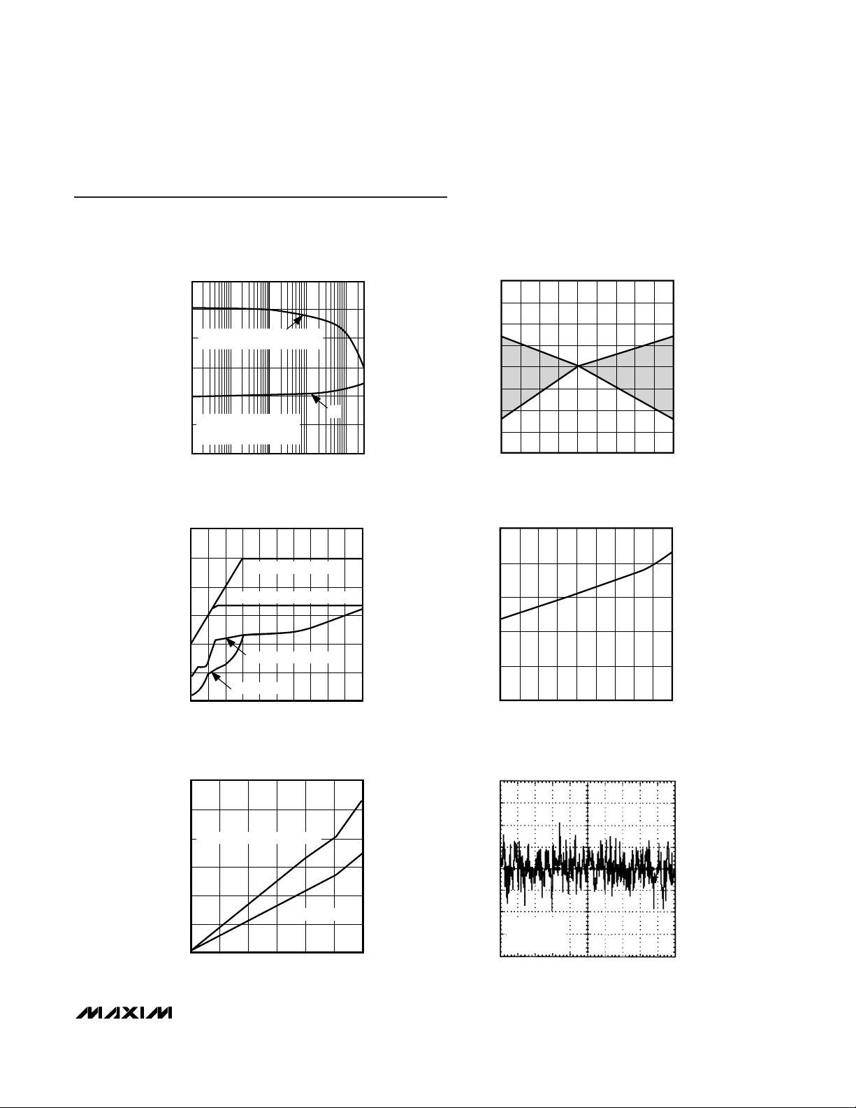
Typical Operating Characteristics
(VIN= 7V for MAX883, VIN = 5.3V for MAX882/MAX884, OFF or STBY = VIN, SET = GND, LBI = VIN, LBO = OPEN, CIN= C
OUT
= 2.2µF,
R
L
= 1kΩ, TA = +25°C, unless otherwise noted.)
95
101
100
99
98
97
96
0.01 0.1 1 10010 250
OUTPUT VOLTAGE AND QUIESCENT
CURRENT vs. LOAD CURRENT
MAX882/4-01
LOAD CURRENT (mA)
NORMALIZED OUTPUT VOLTAGE (%)
V
OUT
= 5V (MAX883)
V
OUT
= 3.3V (MAX882/MAX884)
OUTPUT VOLTAGE
NORMALIZED TO OUTPUT
VOLTAGE AT 1mA
0
5
10
15
20
25
30
QUIESCENT CURRENT (µA)
I
Q
0
2
3
4
5
6
4
6
8
10
12
14
16
OUTPUT VOLTAGE AND QUIESCENT
CURRENT vs. SUPPLY VOLTAGE
MAX882/4-03
SUPPLY VOLTAGE (V)
OUTPUT VOLTAGE (V)
QUIESCENT CURRENT (µA)
2 3 4 5 6 7 8 9 10 11 12
V
OUT
= 5V (MAX883)
V
OUT
= 3.3V (MAX882/MAX884)
IQ (MAX882/MAX884)
IQ (MAX883)
1
0
0.1
0.2
0.3
0.4
0.5
0.6
DROPOUT VOLTAGE
vs. LOAD CURRENT
MAX882/4-05
LOAD CURRENT (mA)
DROPOUT VOLTAGE (V)
0 50 100 150 200 250 300
V
OUT
= 3.3V (MAX882/MAX884)
V
OUT
= 5V (MAX883)
0
15
12
9
6
3
QUIESCENT CURRENT
vs. TEMPERATURE
MAX882/4-04
TEMPERATURE (°C)
QUIESCENT CURRENT (µA)
-55 -35 -15 5 25 45 65 85 105 125
10Hz to 10kHz OUTPUT NOISE
10ms/div
OUTPUT NOISE (1mV/div)
MAX883
V
OUT
= 5V
MAX882/4-06
96
97
98
99
100
101
102
103
104
OUTPUT VOLTAGE
vs. TEMPERATURE
MAX882/4-04a
TEMPERATURE (°C)
NORMALIZED OUTPUT VOLTAGE (%)
-55 -35 -15 5 25 45 65 85 105 125
Page 6

MAX882/MAX883/MAX884
5V/3.3V or Adjustable, Low-Dropout,
Low IQ, 200mA Linear Regulators
6 _______________________________________________________________________________________
LINE-TRANSIENT RESPONSE
500µs/div
MAX883: V
OUT
= 5V, CIN = 0µF, tR = 15µs, tF = 13µs
A: V
IN
= 8V (HIGH) / VIN = 7V (LOW)
B: OUTPUT VOLTAGE (100mV/div)
B
A
LOAD-TRANSIENT RESPONSE
1ms/div
MAX883: V
OUT
= 5V, tR = 24µs, tF = 44µs
A: OUTPUT VOLTAGE (100mV/div)
B: I
OUT
= 250mA (HIGH) / I
OUT
= 50mA (LOW)
B
A
OVERSHOOT AND TIME
EXITING SHUTDOWN MODE
RL = 100Ω
500µs/div
A: OFF PIN VOLTAGE (1V/div):
RISE TIME = 9µs
B: MAX883 OUTPUT VOLTAGE (1V/div):
DELAY = 135µs, RISE TIME = 67µs,
OVERSHOOT = 0%
0V
5V
A
B
0
1
2
3
4
5
0.1 1 10 50
LBO LOW VOLTAGE
vs. SINK CURRENT
MAX882/4-10
SINK CURRENT (mA)
LBO LOW VOLTAGE (V)
MAX882/MAX884
MAX883
Typical Operating Characteristics (continued)
(VIN= 7V for MAX883, VIN= 5.3V for MAX882/MAX884, OFF or STBY = VIN, SET = GND, LBI = VIN, LBO = OPEN, CIN= C
OUT
= 2.2µF,
R
L
= 1kΩ, TA = +25°C, unless otherwise noted.)
Page 7

MAX882/MAX883/MAX884
5V/3.3V or Adjustable, Low-Dropout,
Low IQ, 200mA Linear Regulators
_______________________________________________________________________________________ 7
_______________Detailed Description
The MAX882/MAX883/MAX884 are micropower, lowdropout linear regulators designed primarily for batterypowered applications. They feature Dual Mode operation,
allowing a fixed output of 5V for the MAX883 and 3.3V for
the MAX882/MAX884, or an adjustable output from 1.25V
to 11V. These devices supply up to 200mA while requiring
less than 15µA quiescent current. As illustrated in Figure
1, they consist of a 1.20V reference, error amplifier, MOSFET driver, P-channel pass transistor, dual-mode comparator, and feedback voltage-divider.
The 1.20V reference is connected to the error amplifier’s
inverting input. The error amplifier compares this reference with the selected feedback voltage and amplifies
the difference. The MOSFET driver reads the error signal
and applies the appropriate drive to the P-channel pass
transistor. If the feedback voltage is lower than the reference, the pass transistor’s gate is pulled lower, allowing
more current to pass and increasing the output voltage. If
the feedback voltage is too high, the pass transistor gate
is pulled up, allowing less current to pass to the output.
The output voltage is fed back through either an internal resistor voltage-divider connected to the OUT pin,
or an external resistor network connected to the SET
pin. The dual-mode comparator examines the SET pin
voltage and selects the feedback path used. If the SET
pin is below 65mV, internal feedback is used and the
output voltage is regulated to 5V for the MAX883 or
3.3V for the MAX882/MAX884. Additional blocks
include a foldback current limiter, reverse-current protection, a thermal sensor, shutdown or standby logic,
and a low-battery-detection comparator.
Internal P-Channel Pass Transistor
The MAX882/MAX883/MAX884 feature a 200mA Pchannel MOSFET pass transistor. This provides several
advantages over similar designs using PNP pass transistors, including longer battery life.
The P-channel MOSFET requires no base drive, which
reduces quiescent current considerably. PNP-based regulators waste large amounts of current in dropout when
the pass transistor saturates. They also use high basedrive currents under large loads. The MAX882/MAX883/
MAX884 do not suffer from these problems and consume
only 11µA of quiescent current during light loads, heavy
loads, and dropout.
Output Voltage Selection
The MAX882/MAX883/MAX884 feature Dual Mode
operation. In preset voltage mode, the MAX883’s output is set to 5V and the MAX882/MAX884’s output is set
to 3.3V, using internal trimmed feedback resistors.
Select this mode by connecting SET to ground.
In preset voltage mode, impedances between SET and
ground should be less than 100kΩ. Otherwise, spurious
conditions could cause the voltage at SET to exceed
the 65mV dual-mode threshold.
Pin Description
LBO
SET
GND
OUT
LBI
OFF
STBY
IN
1 1
Low-Battery Output is an open-drain output that goes low when LBI is less than 1.2V. Connect to
IN or OUT through a pull-up resistor. LBO is undefined during shutdown mode
(MAX883/MAX884).
2 2
Feedback for setting the output voltage. Connect to GND to set the output voltage to the preselected 3.3V or 5V. Connect to an external resistor network for adjustable-output operation.
3, 6 3, 6
Ground pins—also function as heatsinks in the SO package. All GND pins must be soldered to
the PC board for proper power dissipation. Connect to large copper pads or planes to
channel heat from the IC.
4 4
Regulator Output. Fixed or adjustable from 1.25V to 11.0V. Sources up to 200mA. Bypass with a
2.2µF capacitor.
8 8 Low-Battery comparator Input. Tie to IN when not used.
— 7
Shutdown. Active-low logic input. In OFF mode, supply current is reduced below 1µA and
V
OUT
= 0.
7 —
Standby. Active-low comparator input. Connect to GND to disable the output or to IN for normal
operation. A resistor network (from IN) can be used to set a standby mode threshold.
5 5 Regulator Input. Supply voltage can range from 2.7V to 11.5V.
NAME
PIN
FUNCTION
MAX883/
MAX884
MAX882
Page 8

MAX882/MAX883/MAX884
5V/3.3V or Adjustable, Low-Dropout,
Low IQ, 200mA Linear Regulators
8 _______________________________________________________________________________________
In adjustable mode, the user selects an output voltage
in the 1.25V to 11V range by connecting two external
resistors, used as a voltage-divider, to the SET pin
(Figure 2).
The output voltage is set by the following equation:
where V
SET
= 1.20V.
To simplify resistor selection:
Since the input bias current at SET is nominally zero,
large resistance values can be used for R1 and R2 to
minimize power consumption without losing accuracy.
Up to 1.5MΩ is acceptable for R2. Since the V
SET
tolerance is less than ±40mV, the output can be set using
fixed resistors instead of trim pots.
Standby Mode (MAX882)
The MAX882 has a standby feature that disconnects
the input from the output when STBY is brought low, but
keeps all other circuitry awake. In this mode, V
OUT
drops to 0, and the internal biasing circuitry (including
the low-battery comparator) remains on. The maximum
quiescent current during standby is 15µA. STBY is a
comparator input with the other input internally tied to
the reference voltage. Use a resistor network as shown
in Figure 3 to set a standby-mode threshold voltage for
undervoltage lockout. Connect STBY to IN for normal
operation.
OFF Mode (MAX883/MAX884)
A low-logic input on the OFF pin shuts down the
MAX883/MAX884. In this mode, the pass transistor,
control circuit, reference, and all biases are turned off,
and the supply current is reduced to less than 1µA.
LBO is undefined in OFF mode. Connect OFF to IN for
normal operation.
R1 R2
V
V
1
OUT
SET
=−
⎛
⎝
⎜
⎞
⎠
⎟
VV
R
R
OUT SET
=+
⎛
⎝
⎜
⎞
⎠
⎟
1
1
2
Figure 1. MAX882/MAX883/MAX884 Functional Diagram
P
OUT
SET
R1
R2
65mV
ERROR AMP
OFF
(STBY)
GND
LBO
LBI
N
IN
MOSFET DRIVER
WITH FOLDBACK
CURRENT LIMIT
REVERSECURRENT
PROTECTION
SHUTDOWN
LOGIC
1.20V
REFERENCE
THERMAL
SENSOR
( ) ARE FOR MAX882.
DUAL-MODE
COMPARATOR
LOW-BATTERY
COMPARATOR
Page 9

MAX882/MAX883/MAX884
5V/3.3V or Adjustable, Low-Dropout,
Low IQ, 200mA Linear Regulators
_______________________________________________________________________________________ 9
Foldback Current Limiting
The MAX882/MAX883/MAX884 also include a foldback
current limiter. It monitors and controls the pass transistor’s gate voltage, estimating the output current and
limiting it to 430mA for output voltages above 0.8V and
(VIN- V
OUT
) > 0.7V. If the output voltage drops below
0.8V, implying a short-circuit condition, the output current is limited to 170mA. The output can be shorted to
ground for 1min without damaging the device if the
package can dissipate (VINx 170mA) without exceeding TJ= +150°C. When the output is greater than 0.8V
and (VIN- V
OUT
) < 0.7V (dropout operation), no current
limiting is allowed, to provide maximum load drive.
Thermal Overload Protection
Thermal overload protection limits total power dissipation in the MAX882/MAX883/MAX884. When the junction temperature exceeds TJ= +160°C, the thermal
sensor sends a signal to the shutdown logic, turning off
the pass transistor and allowing the IC to cool. The
thermal sensor turns the pass transistor on again after
the IC’s junction temperature cools by 10°C, resulting in
a pulsed output during thermal overload conditions.
Thermal overload protection is designed to protect the
MAX882/MAX883/MAX884 if fault conditions occur. It is
not intended to be used as an operating mode.
Prolonged operation in thermal-shutdown mode may
reduce the IC’s reliability. For continual operation, do
not exceed the absolute maximum junction temperature
rating of TJ= +150°C.
Power Dissipation and Operating Region
Maximum power dissipation of the MAX882/MAX883/
MAX884 depends on the thermal resistance of the case
and PC board, the temperature difference between the
die junction and ambient air, and the rate of
air flow. The power dissipation across the device is
P = I
OUT(VIN
- V
OUT
). The resulting power dissipation
is as follows:
where (TJ - TA) is the temperature difference between
the MAX882/MAX883/MAX884 die junction and the surrounding air, θJB(or θJC) is the thermal resistance of
the package chosen, and θBAis the thermal resistance
through the PC board, copper traces, and other materials to the surrounding air.
The 8-pin small-outline package for the MAX882/
MAX883/MAX884 features a special lead frame with a
lower thermal resistance and higher allowable power
dissipation. This package’s thermal resistance package
is θJB= 53°C/W, compared with θJB= 110°C/W for an
8-pin plastic DIP package and θJB= 125°C/W for an 8pin ceramic DIP package.
P
(T T )
()
JA
JB BA
=
−
+θθ
Figure 2. Adjustable Output Using External Feedback
Resistors
Figure 3. Setting an Undervoltage Lockout Threshold Using
STBY
MAX882
MAX883
MAX884
C
IN
O.1µF
C
OUT
2.2µF
OUTPUT
VOLTAGE
INPUT
VOLTAGE
LBI
OFF
(STBY)
( ) ARE FOR MAX882.
IN
R1
R2
R1 + R2
R2
V
OUT
= V
SET
, V
SET
= 1.20V
LOAD
OUT
GND
SET
C
OUT
2.2µF
OUTPUT
VOLTAGE
STBY
R1+ R2
R2
IN
LBI
STBY
, V
STBY
MAX882
GND
= 1.20V
INPUT
VOLTAGE
R1
C
IN
STBY TRIP
R2
= V
O.1µF
V
OUT
SET
Page 10

MAX882/MAX883/MAX884
5V/3.3V or Adjustable, Low-Dropout,
Low IQ, 200mA Linear Regulators
10 ______________________________________________________________________________________
The GND pins of the MAX882/MAX883/MAX884 SOIC
package perform the dual function of providing an electrical connection to ground and channeling heat away. Connect all GND pins to ground using a large pad or ground
plane. Where this is impossible, place a copper plane on an
adjacent layer. For a given power dissipation, the pad
should exceed the associated dimensions in Figure 4.
Figure 4 assumes the IC is in an 8-pin small-outline package that has a maximum junction temperature of +125°C
and is soldered directly to the pad; it also has a +25°C
ambient air temperature and no other heat sources. Use
larger pad sizes for other packages, lower junction temperatures, higher ambient temperatures, or conditions
where the IC is not soldered directly to the heat-sinking
ground pad. When operating C- and E-grade parts up to a
TJof +125°C, expect performance similar to M-grade
specifications. For TJ between +125°C and +150°C, the
output voltage may drift more.
The MAX882/MAX883/MAX884 can regulate currents up
to 250mA and operate with input voltages up to 11.5V, but
not simultaneously. High output currents can only be sustained when input-output differential voltages are small, as
shown in Figure 5. Maximum power dissipation depends
on packaging, temperature, and air flow. The maximum
output current is as follows:
where P is derived from Figure 4.
I
P(T T )
(V V )100 C
OUT(MAX)
JA
IN OUT
=
−
−°
1.0
0.9
1.6
1.5
1.4
1.3
1.2
1.1
0.1cm
2
0.0155in
2
1cm
2
0.155in
2
10cm
2
1.55in
2
100cm
2
15.5in
2
MAX882/4-fig04
COPPER GROUND PAD AREA
POWER DISSIPATION (W)
MAX883, V
OUT
= 5V
8-PIN SO PACKAGE
77.4cm
2
,
SINGLE-SIDED BOARD
1oz COPPER
GLASS EPOXY,
T
J
= +125°C,
T
A
= +25°C, STILL AIR
Figure 4. Typical Maximum Power Dissipation vs. Ground Pad
Area
Figure 5a. Safe Operating Regions: MAX882/MAX884 Maximum
Output Current vs. Supply Voltage
Figure 5b. Safe Operating Regions: MAX883 Maximum Output
Current vs. Supply Voltage
250
MAXIMUM CURRENT
200
150
PLASTIC DIP
100
50
MAXIMUM OUTPUT CURRENT (mA)
0
CERAMIC DIP
OPERATING
REGION AT
TA = +25°C
T
= +125°C
TYPICAL DROPOUT VOLTAGE LIMIT
J
5432768109111312
SUPPLY VOLTAGE (V)
MAXIMUM POWER
DISSIPATION LIMIT
HIGH-
POWER
SOIC
MAX882/4-05a
MAXIMUM SUPPLY VOLTAGE LIMIT
250
MAXIMUM CURRENT
200
150
100
50
MAXIMUM OUTPUT CURRENT (mA)
0
PLASTIC DIP
OPERATING
REGION AT
TA = +25°C
TJ = +125°C
TYPICAL DROPOUT VOLTAGE LIMIT
54768109111312
SUPPLY VOLTAGE (V)
MAXIMUM POWER
DISSIPATION LIMIT
CERAMIC DIP
HIGH-
POWER
SOIC
MAX882/4-05b
MAXIMUM SUPPLY VOLTAGE LIMIT
Page 11

MAX882/MAX883/MAX884
5V/3.3V or Adjustable, Low-Dropout,
Low IQ, 200mA Linear Regulators
______________________________________________________________________________________ 11
Reverse-Current Protection
The MAX882/MAX883/MAX884 have a unique protection
scheme that limits reverse currents when the input voltage falls below the output. It monitors the voltages on IN
and OUT and switches the IC’s substrate and power bus
to the more positive of the two. The control circuitry is
then able to remain functioning and turn the pass transistor off, limiting reverse currents back through to the input
of the device. In this mode, typical current into OUT to
GND is 15µA at V
OUT
= 3.3V and 50µA at V
OUT
= 5V.
Reverse-current protection activates when the voltage
on IN falls 6mV (or 20mV max) below the voltage on
OUT. Before this happens, currents as high as several
milliamperes can flow back through the device.
Low-Battery-Detection Comparator
The MAX882/MAX883/MAX884 provide a low-battery comparator that compares the voltage on the LBI pin to the
1.20V internal reference. LBO, an open-drain output, goes
low when LBI is below 1.20V. Hysteresis of 7mV has been
added to the low-battery comparator to provide noise
immunity during switching. LBO remains functional in standby mode for the MAX882, but is undefined in OFF mode for
the MAX883 and MAX884. Tie LBI to IN when not used.
Use a resistor-divider network as shown in Figure 6 to set
the low-battery trip voltage. Current into the LBI input is
±50nA (max), so R2 can be as large as 1MΩ. Add extra
noise immunity by connecting a small capacitor from LBI
to GND. Additional hysteresis can be added by connecting a high-value resistor from LBI to LBO.
Applications Information
The MAX882/MAX883/MAX884 are series linear regulators designed primarily for battery-powered systems.
Figure 7 shows a typical application.
Standby Mode vs. OFF Mode
STBY is a comparator input that allows the user to set
the standby-mode threshold voltage, while OFF is a
logic-level input. When in standby mode, the output is
disconnected from the input, but the biasing circuitry
(including the low-battery comparator) is kept alive,
causing the device to draw approximately 7µA.
Standby mode is useful in applications where a lowbattery comparator function is still needed in shutdown.
A logic low at the OFF pin turns off all biasing circuitry,
including the LBI/LBO comparator, and reduces supply
current to less than 1µA. OFF mode is useful for maximizing battery life. There is little difference in the time it
takes to exit standby mode or OFF mode.
Output Capacitor Selection
and Regulator Stability
An output filter capacitor is required at the MAX882/
MAX883/MAX884 OUT pin. The minimum output
capacitance required for stability is 2.2µF.
MAX882
MAX883
MAX884
C
IN
O.1µF
C
OUT
2.2µF
OUTPUT
VOLTAGE
BATTERY
LBOLBI
OFF (STBY)
( ) ARE FOR MAX882.
IN
POWERFAIL
INDICATION
R3
R1 + R2
R2
V
LBI TRIP
= V
LBI
, V
LBI
= 1.20V
OUT
GND
SET
R1
R2
Figure 6. Using the Low-Battery Comparator to Monitor Battery
Voltage
Figure 7. Typical 3.3V or 5V Linear Regulator Circuit
OFF (STBY)ON/OFF
INPUT
VOLTAGE
BATTERY
* OPTIONAL REVERSE BATTERY PROTECTION
*
C
IN
O.1µF
( ) ARE FOR MAX882.
IN
LBI
SET
MAX882
MAX883
MAX884
GND
OUT
OUTPUT
VOLTAGE
C
OUT
2.2µF
Page 12

MAX882/MAX883/MAX884
5V/3.3V or Adjustable, Low-Dropout,
Low IQ, 200mA Linear Regulators
12 ______________________________________________________________________________________
The filter capacitor’s size depends primarily on the
desired power-up time and load-transient responses.
Load-transient response is improved by using larger
output capacitors.
The output capacitor’s equivalent series resistance
(ESR) will not affect stability as long as the minimum
capacitance requirement is observed. The type of
capacitor selected is not critical, but it must remain
above the minimum value over the full operating temperature range.
Input Bypass Capacitor
Normally, use 0.1µF to 10µF capacitors on the MAX882/
MAX883/MAX884 input. The best value depends primarily on the power-up slew rate of VIN, and on load
and line transients. Larger input capacitor values provide better supply-noise rejection and line-transient
response, as well as improved performance, when the
supply has a high AC impedance. The type of input
bypass capacitor used is not critical.
Noise
The MAX882/MAX883/MAX884 exhibit up to 4mV
p-p
of
noise during normal operation. This is negligible in
most applications. When using the MAX882/MAX883/
MAX884 for applications that include analog-to-digital
converters (ADCs) with resolutions greater than 12 bits,
consider the ADC’s power-supply rejection specifications. See the output noise plot in the Typical Operating
Characteristics section.
PSRR and Operation from
Sources Other than Batteries
The MAX882/MAX883/MAX884 are designed to
achieve low dropout voltages and low quiescent currents in battery-powered systems. However, to gain
these benefits, the devices must trade away powersupply noise rejection, as well as swift response to supply variations and load transients. For a 1mA load
current, power-supply rejection ranges from 60dB
down to 20dB at 2kHz. At higher frequencies, the circuit depends primarily on the characteristics of the output capacitor, and the PSRR increases (Figure 8).
0
60
50
40
30
20
10
10
1
10210310410
5
10
6
MAX882/4-8b
FREQUENCY (Hz)
PSRR (dB)
A: C
OUT
= 1µF
B: C
OUT
= 10µF
C: C
OUT
= 100µF
A
B
C
MAX883
∆VIN = 1V
P-P
CIN = 0µF
I
OUT
= 100mA
Figure 8b. Power-Supply Rejection Ratio vs. Ripple Frequency
for Various Output Capacitances
Figure 8a. Power-Supply Rejection Ratio vs. Ripple Frequency
for Light and Heavy Loads
80
70
60
50
40
PSRR (dB)
30
MAX884
20
∆VIN = 1V
P-P
CIN = 0µF
10
C
= 2.2µF
OUT
0
0101102103104105106
10
I
OUT
FREQUENCY (Hz)
= 1mA
I
OUT
= 100mA
MAX882/4-8a
Page 13

MAX882/MAX883/MAX884
5V/3.3V or Adjustable, Low-Dropout,
Low IQ, 200mA Linear Regulators
______________________________________________________________________________________ 13
When operating from sources other than batteries, supply-noise rejection and transient response can be
improved by increasing the values of the input and output capacitors and employing passive filtering techniques. Do not use power supplies with ripple voltage
exceeding 200mV at 100kHz.
Overshoot and Transient Considerations
The Typical Operating Characteristics section shows
power-up, supply, and load-transient response graphs.
On the load-transient graphs, two components of the
output response can be observed: a DC shift from the
output impedance due to the different load currents,
and the transient response. Typical transients for step
changes in the load current from 50mA to 250mA are
200mV. Increasing the output capacitor’s value attenuates transient spikes.
During recovery from shutdown, overshoot is negligible
if the output voltage has been given time to decay adequately. During power-up from VIN= 0, overshoot is
typically less than 1% of V
OUT
.
Input-Output (Dropout) Voltage
A regulator’s minimum input-output voltage differential
(or dropout voltage) determines the lowest usable supply voltage. In battery-powered systems, this determines the useful end-of-life battery voltage. Because
the MAX882/MAX883/MAX884 use a P-channel MOSFET pass transistor, their dropout voltage is a function
of R
DS(ON)
multiplied by the load current (see Electrical
Characteristics). Quickly stepping up the input voltage
from the dropout voltage can result in overshoot.
Short-Term Battery Backup
Using the MAX882
Figure 9 illustrates a scheme for implementing battery
backup for 3.3V circuits using the MAX882. When the
supply voltage drops below some user-specified value
based on resistors R1 and R2, the standby function
activates, turning off the MAX882’s output. Under
these conditions, the backup battery supplies power to
the load. Reverse current protection prevents the battery from draining back through the regulator to the
input.
This application is limited to short-term battery backup
for 3.3V circuits. The current drawn by the MAX882’s
OUT pin at 3.3V during reverse-current protection is
typically 8µA. It should not be used with the MAX883
and MAX884, since the OFF pin is a logic input, and
indeterminate inputs can cause the regulator to turn on
intermittently, draining the battery.
Reverse Battery Protection
Reverse battery protection can be added by including
an inexpensive Schottky diode between the battery
input and the regulator circuit, as shown in Figure 7.
However, the dropout voltage of the regulator will be
increased by the forward voltage drop of the diode. For
example, the forward voltage of a standard 1N5817
Schottky diode is typically 0.29V at 200mA.
BACKUP
BATTERY
MAX882
C
IN
O.1µF
C
OUT
2.2µF
OUTPUT
VOLTAGE
INPUT
VOLTAGE
LBI
SET
STBY
IN
D2
R1
R2
OUT
GND
Figure 9. Short-Term Battery Backup Using the MAX882
Page 14

MAX882/MAX883/MAX884
5V/3.3V or Adjustable, Low-Dropout,
Low IQ, 200mA Linear Regulators
14 ______________________________________________________________________________________
Ordering Information (continued) ___________________Chip Topography
*Dice are tested at TJ= +25°C, DC parameters only.
SET
OUT
IN
0.085"
(2.159mm)
0.080"
(2.032mm)
OUT
LBI
OFF (MAX883/4)
STBY (MAX882)
GNDLB0
TRANSISTOR COUNT: 151
NO DIRECT SUBSTRATE CONNECTION. THE N-SUBSTRATE IS INTERNALLY SWITCHED BETWEEN THE
MORE POSITIVE OF IN OR OUT.
PART
TEMP RANGE
PIN-
PACKAGE
PKG
CODE
MAX883CPA 0°C to +70°C 8 PDIP P8-2
MAX883CSA 0°C to +70°C 8 SO S8-6F
MAX883C/D 0°C to +70°C Dice* —
MAX883EPA
8 PDIP P8-2
MAX883ESA
8 SO S8-6F
MAX884CPA 0°C to +70°C 8 PDIP P8-2
MAX884CSA 0°C to +70°C 8 SO S8-6F
MAX884C/D 0°C to +70°C Dice* —
MAX884EPA
8 PDIP P8-2
MAX884ESA
8 SO S8-6F
Revision History
Pages changed at Rev 2: 1–4, 14, 15
-40°C to +85°C
-40°C to +85°C
-40°C to +85°C
-40°C to +85°C
Page 15

MAX882/MAX883/MAX884
5V/3.3V or Adjustable, Low-Dropout,
Low IQ, 200mA Linear Regulators
______________________________________________________________________________________ 15
PDIPN.EPS
Package Information
(The package drawing(s) in this data sheet may not reflect the most current specifications. For the latest package outline information,
go to www.maxim-ic.com/packages
.)
Page 16

Maxim cannot assume responsibility for use of any circuitry other than circuitry entirely embodied in a Maxim product. No circuit patent licenses are
implied. Maxim reserves the right to change the circuitry and specifications without notice at any time.
16 __________________Maxim Integrated Products, 120 San Gabriel Drive, Sunnyvale, CA 94086 (408) 737-7600
© 2000 Maxim Integrated Products is a registered trademark of Maxim Integrated Products, Inc.
MAX882/MAX883/MAX884
5V/3.3V or Adjustable, Low-Dropout,
Low IQ, 200mA Linear Regulators
Package Information (continued)
(The package drawing(s) in this data sheet may not reflect the most current specifications. For the latest package outline information,
go to www.maxim-ic.com/packages
.)
SOICN .EPS
PACKAGE OUTLINE, .150" SOIC
1
1
21-0041
B
REV.DOCUMENT CONTROL NO.APPROVAL
PROPRIETARY INFORMATION
TITLE:
TOP VIEW
FRONT VIEW
MAX
0.010
0.069
0.019
0.157
0.010
INCHES
0.150
0.007
E
C
DIM
0.014
0.004
B
A1
MIN
0.053A
0.19
3.80 4.00
0.25
MILLIMETERS
0.10
0.35
1.35
MIN
0.49
0.25
MAX
1.75
0.050
0.016L
0.40 1.27
0.3940.386D
D
MINDIM
D
INCHES
MAX
9.80 10.00
MILLIMETERS
MIN
MAX
16
AC
0.337 0.344 AB8.758.55 14
0.189 0.197 AA5.004.80 8
N MS012
N
SIDE VIEW
H 0.2440.228 5.80 6.20
e 0.050 BSC 1.27 BSC
C
HE
e
B
A1
A
D
0∞-8∞
L
1
VARIATIONS:
 Loading...