General Description
The MAX8821 integrates a charge pump for white
LEDs, an audio loudspeaker amplifier, and two lownoise LDOs controlled by an I
2
C control interface. The
high-efficiency, adaptive-mode inverting charge pump
drives up to six LEDs with constant current for uniform
brightness. The LED current is controlled by an I
2
C
interface and adjusts from 0.1mA to 25.6mA per LED
into 32 pseudo-logarithmic steps. Independent voltages for each LED maximize efficiency even with large
LED forward voltage (V
F
) mismatch. An internal temperature derating function reduces the current above
+40°C to protect the LEDs.
The high-efficiency mono Class D audio amplifier delivers up to 2W into a 4Ω speaker from a 5V input supply.
The amplifier features proprietary filterless Active
Emissions Limiting (AEL) technology. AEL prevents
high-frequency emissions resulting from conventional
Class D free-wheeling behavior in the presence of an
inductive load. The amplifier offers two modulation
schemes: a fixed-frequency mode (FFM) and a spreadspectrum mode (SSM) that reduce EMI-radiated emissions due to the modulation frequency. The amplifier
also has robust output protection and high power-supply rejection ratio (PSRR). Click-and-pop suppression is
active during power-up/down, enable/disable, and for
all mode changes. The amplifier’s gain is adjustable
through an I2C interface, from -3dB to +24dB in 10 3dB
steps. Differential inputs improve common-mode noise
rejection.
The LDOs in the MAX8821 are designed for low-noise
operation. Each LDO output voltage can be individually
programmed by the I
2
C interface. Both LDO1 and
LDO2 have a high 70dB PSRR rating.
The MAX8821 includes soft-start, thermal shutdown,
open-circuit, and short-circuit protections, and is available in a compact 28-pin, Thin QFN, 4mm x 4mm package (0.8mm max height).
Applications
Cell Phones and Smartphones
PDAs, Digital Cameras, Camcorders
MP3 Players, GPS Devices
Features
♦ White LED Inverting Charge Pump
Independent Adaptive Current Regulators for
Each LED
6 Low-Dropout Current Regulators
Flexible I2C Dimming Control for Each LED
Ramp-Up/Down, Current Control for Each LED
Low 70µA (typ) Quiescent Current
TADerating Function Protects LEDs
♦ Mono 2W Class D Loudspeaker Amplifier
85% Efficiency (RL= 8Ω, P
OUT
= 600mW)
Low 0.05% THD+N at 1kHz
High 65dB PSRR at 1kHz
Fully Differential Inputs
-3dB to +24dB Gain Settings in 3dB Steps
Integrated Click-and-Pop Suppression
Low Quiescent Current
♦ Dual Low-Noise LDO
45µV
RMS
Output Noise, 70dB PSRR
Flexible I2C-Controlled Output Voltages
200mA and 300mA Output Current Drive
MAX8821
White LED Charge Pump with Mono Class D
Audio Amp and Dual LDO
________________________________________________________________
Maxim Integrated Products
1
19-1014; Rev 0; 10/07
For pricing, delivery, and ordering information, please contact Maxim Direct at 1-888-629-4642,
or visit Maxim's website at www.maxim-ic.com.
Ordering Information
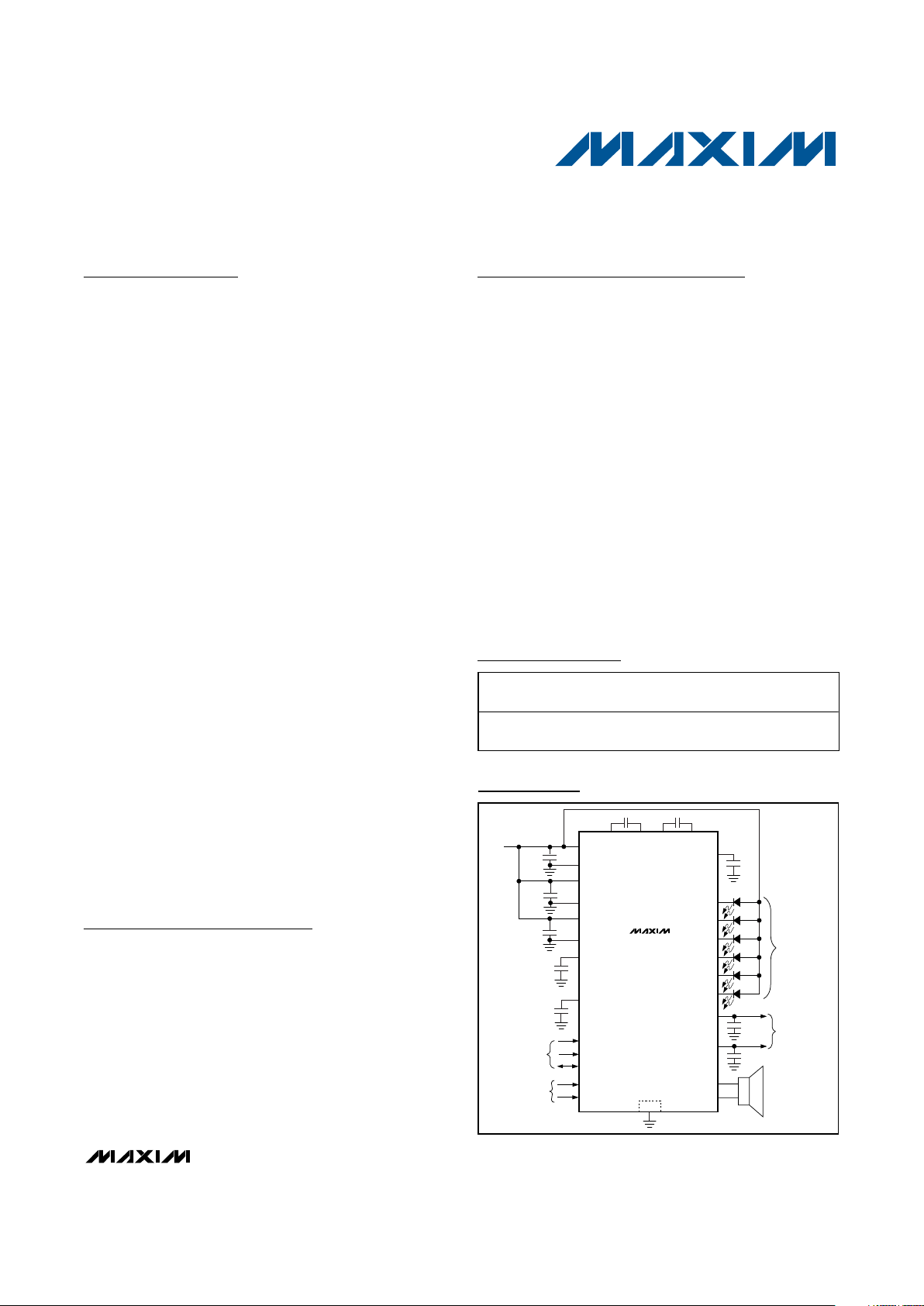
NEG
LED1
LED5
LED4
LED3
LED2
LED6
DUAL LOW
NOISE LDO
LOUDSPEAKER/
EARPIECE
SPK+
SPK-
INDIVIDUAL
0.1mA TO
25.6mA
DIMMING
PGND1
IN1
CMREF
IN3
REF
AGND
IN2
PGND2
AIN+
AIN-
V
DD
SDA
SCL
DIFFERENTIAL
AUDIO INPUT
LOGIC
CONTROL AND I
2
C
INTERFACE
EP
C1P C1N
C2P C2N
LDO1
LDO2
INPUT
2.7 TO 5.5V
MAX8821
Typical Operating Circuit
PART TEMP RANGE
PINPACKAGE
PKG
CODE
MAX8821ETI+ -40°C to +85°C
28 Thin QFN
4mm x 4mm
T2844-1
+
Denotes a lead-free package.
MAX8821
White LED Charge Pump with Mono Class D
Audio Amp and Dual LDO
2 _______________________________________________________________________________________
ABSOLUTE MAXIMUM RATINGS
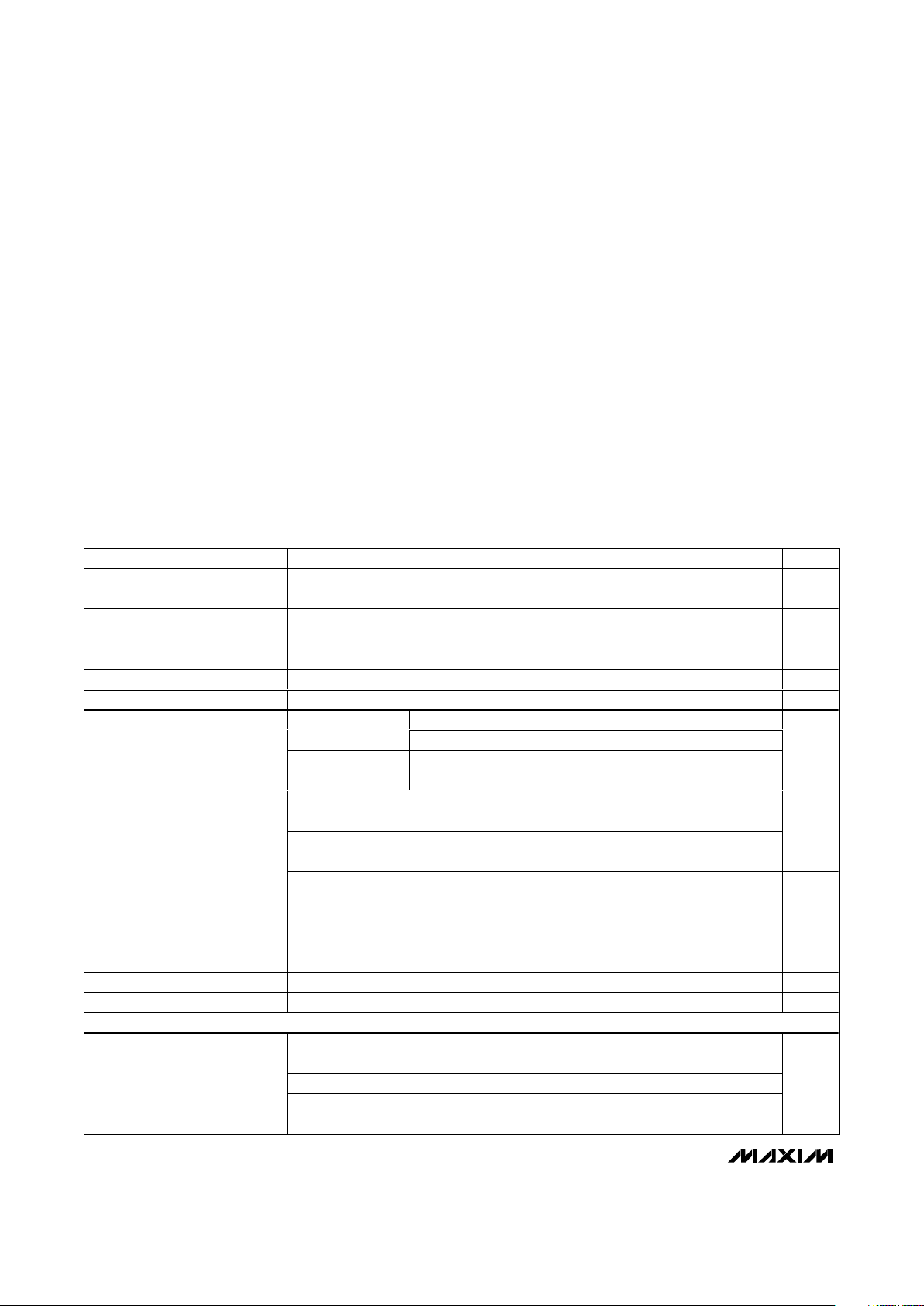
ELECTRICAL CHARACTERISTICS
(V
IN1
= V
IN2
= V
IN3
= VDD= 3.6V, V
AGND
= V
PGND1
= V
PGND2
= 0V, circuit of Figure 2, TA= -40°C to +85°C, unless otherwise noted.
Typical values are at T
A
= +25°C.) (Note 1)
Stresses beyond those listed under “Absolute Maximum Ratings” may cause permanent damage to the device. These are stress ratings only, and functional
operation of the device at these or any other conditions beyond those indicated in the operational sections of the specifications is not implied. Exposure to
absolute maximum rating conditions for extended periods may affect device reliability.
IN1, IN2, IN3, VDDto AGND..................................-0.3V to +6.0V
SCL, SDA to AGND ....................................-0.3V to (V
DD
+ 0.3V)
IN1, IN2, IN3 to NEG .............................................-0.3V to +6.0V
AGND to C2N ........................................................-0.3V to +6.0V
C1P, C2P to AGND ....................................-0.3V to (V
IN1
+ 0.3V)
LED_, C1N, C2N to NEG............................-0.3V to (V
IN1
+ 0.3V)
LDO1, LDO2, REF to AGND ......................-0.3V to (V
IN3
+ 0.3V)
CMREF, AIN+, AIN-, SPK+, SPK-
to AGND..................................................-0.3V to (V
IN2
+ 0.3V)
IN1, IN2 to IN3.......................................................-0.3V to +0.3V
PGND1, PGND2 to AGND.....................................-0.3V to +0.3V
SPK+, SPK- Short Circuit to PGND2 or IN2 ...............Continuous
Continuous Power Dissipation (T
A
= +70°C)
28-Pin, Thin QFN 4mm x 4mm
(derate 28.6mW/°C above +70°C)..............................2286mW
Junction Temperature......................................................+150°C
Storage Temperature Range .............................-65°C to +150°C
Lead Temperature (soldering, 10s) .................................+300°C
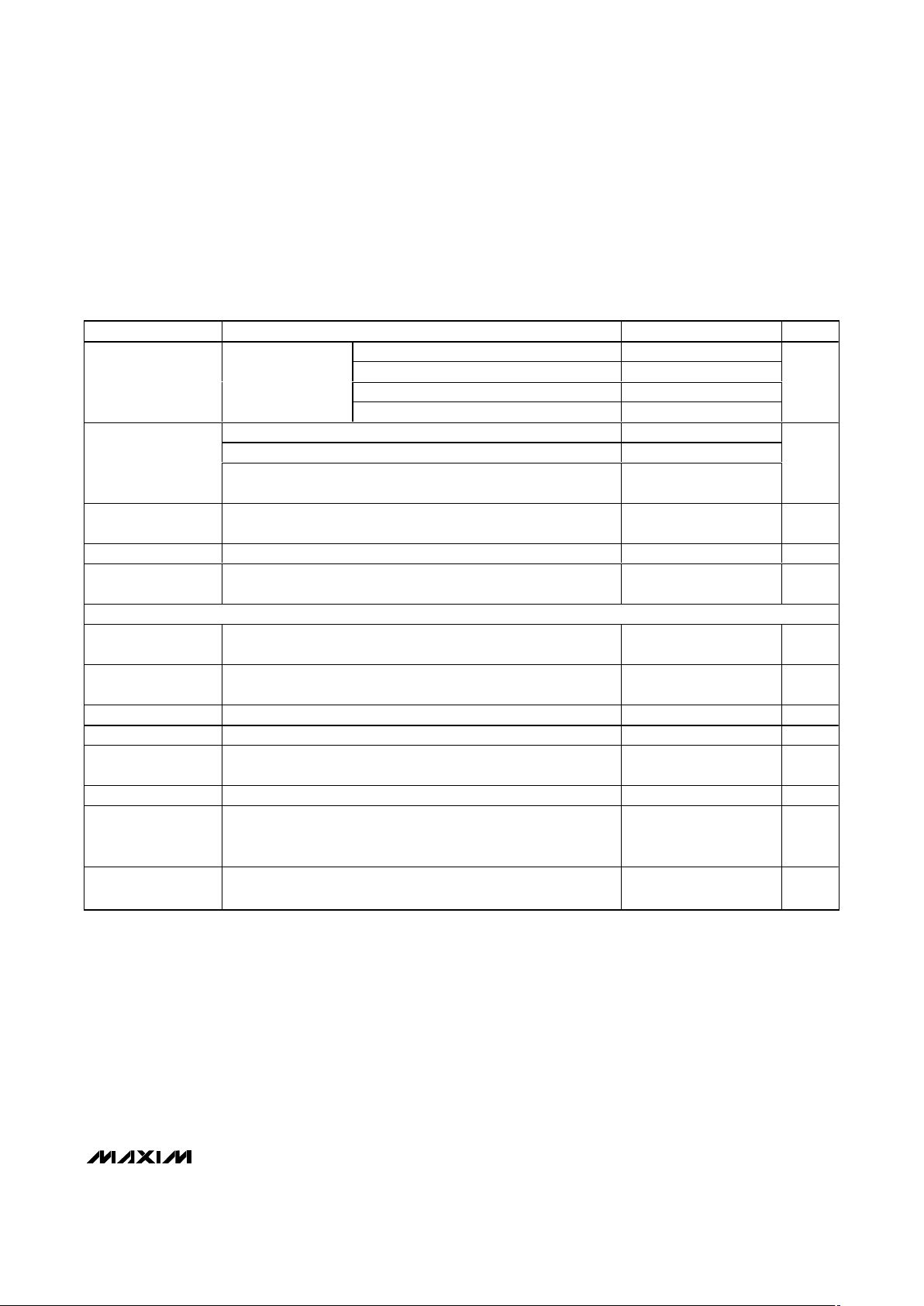
PARAMETER CONDITIONS MIN TYP MAX UNITS
V
IN1
, V
IN2
, V
IN3
Operating
Voltage
2.7 5.5 V
VDD Operating Range 1.5 5.5 V
Undervoltage Lockout (UVLO)
Threshold
V
IN3
rising 2.25 2.45 2.65 V
UVLO Hysteresis 100 mV
VDD Shutdown Threshold 0.450 0.865 1.350 V
TA = +25°C 0.1 1
VDD = AGND
T
A
= +85°C 0.1
TA = +25°C 2 10
IN1, IN2, IN3 Shutdown Supply
Current
(All Outputs Off)
V
DD
= 3.6V
T
A
= +85°C 2
µA
Charge pump inactive, 2 LEDs at 0.1mA setting, audio
amplifier disabled, LDO1 and LDO2 disabled
70 120
LED driver disabled, audio amplifier disabled, and LDO1
and LDO2 enabled
170 250
µA
Charge pump active, 1MHz switching, all LEDs at
25.6mA setting, audio amplifier disabled, LDO1 and
LDO2 disabled
1.50 4.00
No-Load Supply Current
LED driver disabled, audio amplifier enabled, LDO1 and
LDO2 disabled
6.6 20
mA
Thermal Shutdown +160 °C
Thermal-Shutdown Hysteresis 20 °C
CHARGE PUMP
SYNC = 0 1000
SYNC = 1, SW_MODE = 00 450 550 650
SYNC = 1, SW_MODE = 01 575 700 825
Switching Frequency
(f
SW
)
SYNC = 1, SW_MODE = 10
625
± 25
kHz
MAX8821
White LED Charge Pump with Mono Class D
Audio Amp and Dual LDO
_______________________________________________________________________________________ 3
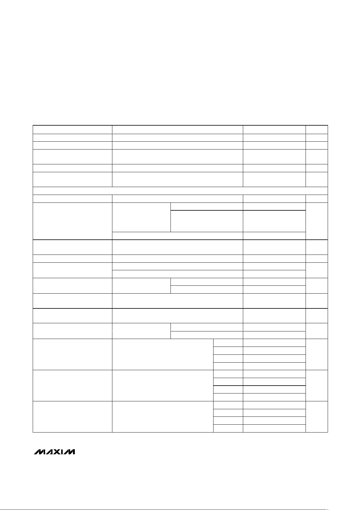
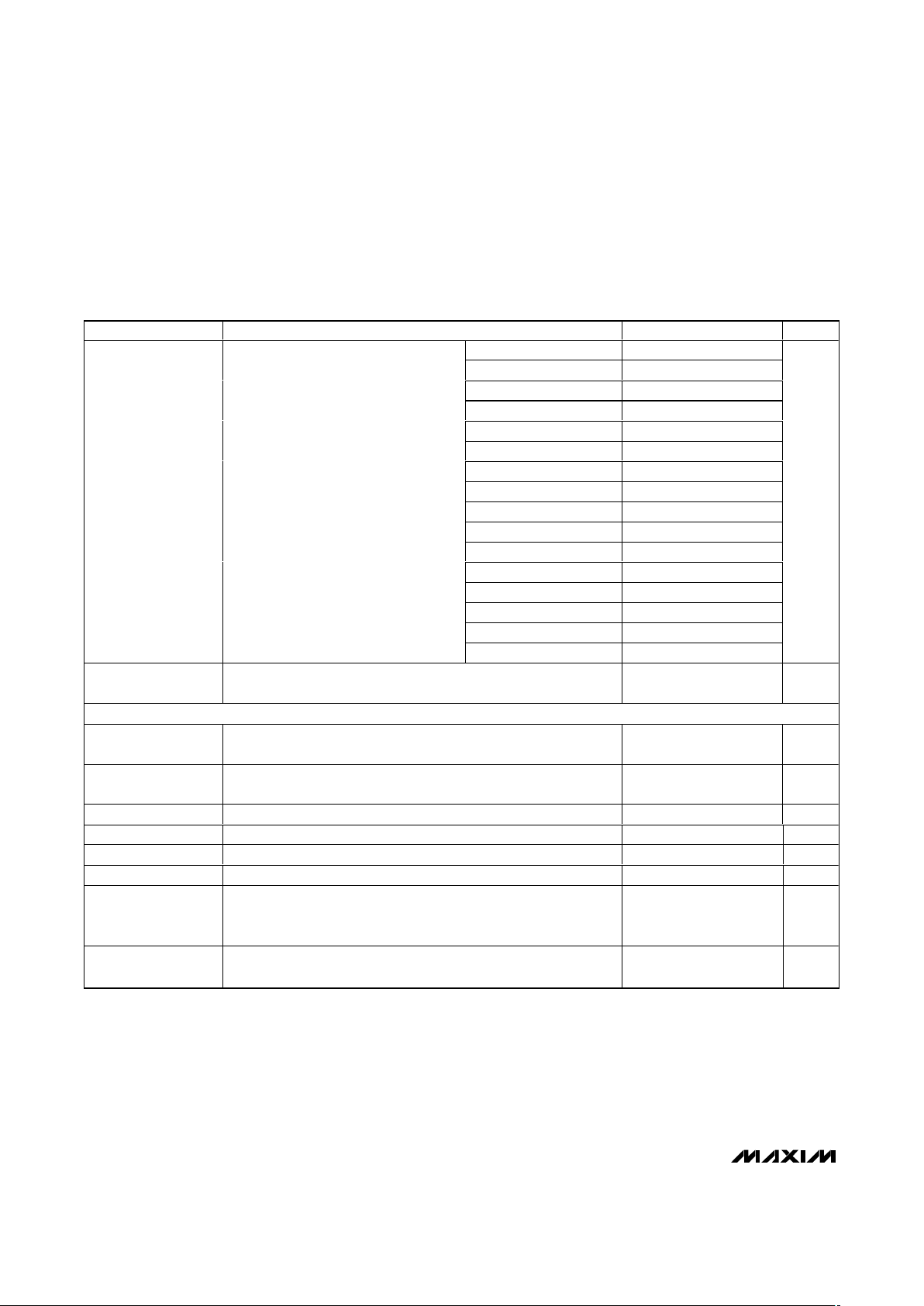
PARAMETER CONDITIONS MIN TYP MAX UNITS
Soft-Start Time 0.1 ms
Regulation Voltage (V
IN1
- V
NEG
)5V
Open-Loop NEG Output
Resistance
(0.5 x V
IN1
- V
NEG
) / I
NEG
1.75 3.5 Ω
Output Current V
IN1
= 3.2V, LED V
FMAX
= 3.9V 154 mA
NEG Discharge Resistance in
Shutdown
All LEDs disabled 10 kΩ
LED_ CURRENT REGULATORS
Current Setting Range I
LED
_ 0.1 25.6 mA
TA = +25°C -2 ±1 +2
25.6mA setting
T
A
= -40°C to derating
function start temperature
(enabled by I
2
C)
-5 +5
Current Accuracy
0.1mA setting, T
A
= +25°C -30 ±5 +30
%
Current-Derating-Function Start
Temperature
+40 °C
Current-Derating-Function Slope TA = +40°C to +85°C -1.67 %/°C
Charge pump inactive 2.3 4.6
R
DS ON
Charge pump active 5 14
Ω
Charge pump inactive 72 120
Dropout Voltage 25.6mA setting (Note 2)
Charge pump active 120 360
mV
Current Regulator
Switchover Threshold
Charge pump inactive to active,
V
LED_
falling
125 150 175 mV
Current Regulator
Switchover Hysteresis
100 mV
TA = +25°C 0.01 1
Leakage Current in Shutdown
All LEDs
disabled
T
A
= +85°C 0.1
µA
00 524
01 1048
10 2097
Off Blink Time
B7, B6 or B3, B2,
SYNC = 0,
Table 11
11 4194
ms
00 66
01 131
10 262
On Blink Time
B5, B4 or B1, B0,
SYNC = 0,
Table 11
11 524
ms
00 262
01 524
10 1048
Ramp-Up/Down Time
LED__RU: B7, B6 or B3, B2
LED__RD: B5, B4 or B1, B0
SYNC = 0,
Tables 8, 9, 10 (Note 3)
11 2097
ms
ELECTRICAL CHARACTERISTICS (continued)
(V
IN1
= V
IN2
= V
IN3
= VDD= 3.6V, V
AGND
= V
PGND1
= V
PGND2
= 0V, circuit of Figure 2, TA= -40°C to +85°C, unless otherwise noted.
Typical values are at T
A
= +25°C.) (Note 1)
MAX8821
White LED Charge Pump with Mono Class D
Audio Amp and Dual LDO
4 _______________________________________________________________________________________
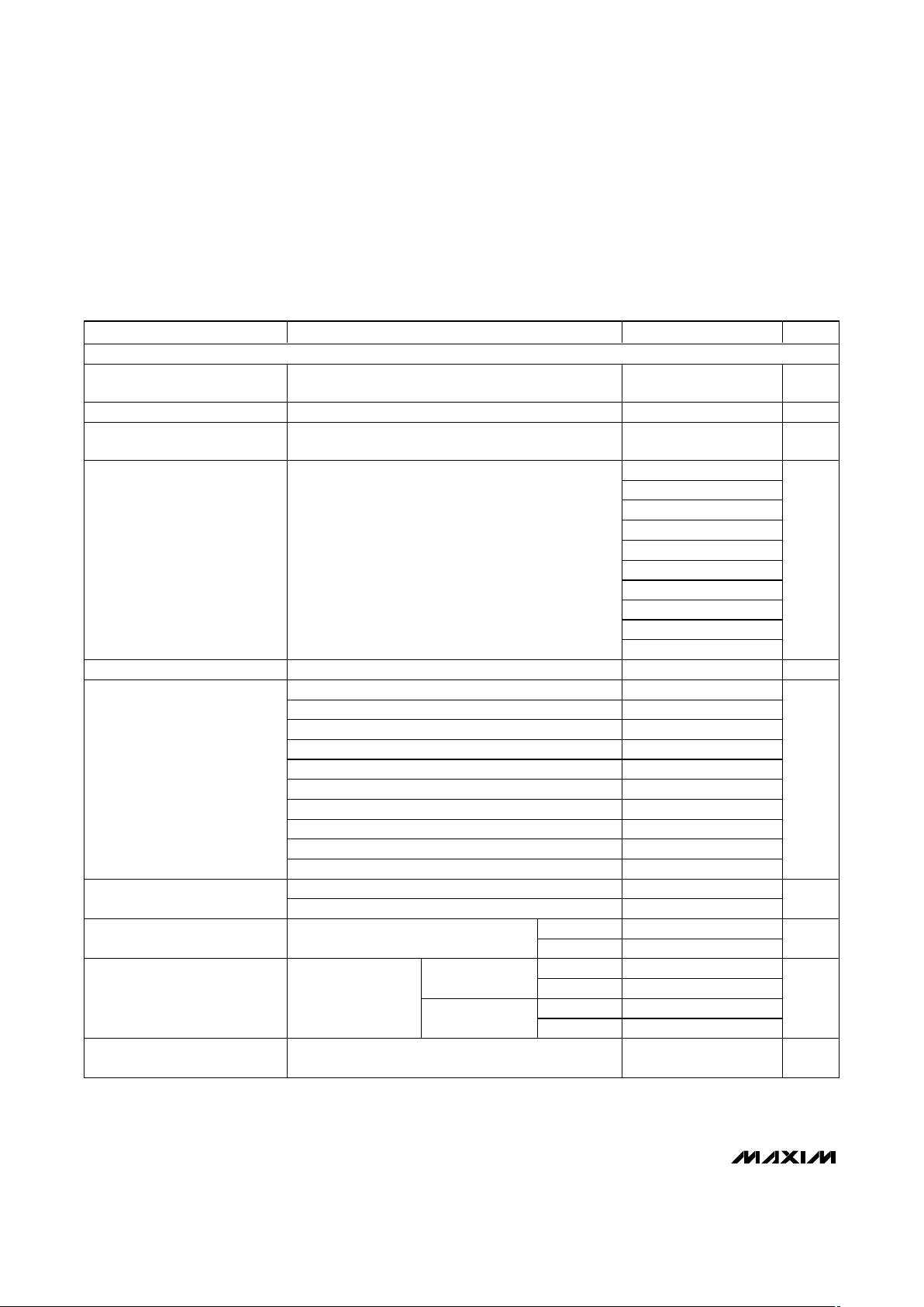
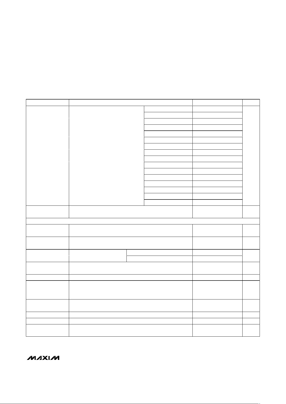
PARAMETER CONDITIONS MIN TYP MAX UNITS
AUDIO AMPLIFIER
Common-Mode Bias Voltage
0.95 x
(V
IN3
/ 2)
V
IN3
/ 2
1.05 x
(V
IN3
/ 2)
V
Output Offset Voltage V
AIN+
= V
AIN-
= V
IN3
/ 2, audio gain = 0dB ±1 mV
Common-Mode Input Voltage 0.5
V
IN3
-
1.2V
V
-3
0
3
6
9
12
15
18
21
Audio Gain Table 15, B3:B0
24
dB
Audio Gain Accuracy -3 +3 %
Audio gain = -3dB 54.4 99.0 143.5
Audio gain = 0dB 49.1 89.2 129.3
Audio gain = 3dB 43.1 78.4 113.7
Audio gain = 6dB 36.8 66.9 97.0
Audio gain = 9dB 30.5 55.5 80.5
Audio gain = 12dB 24.6 44.7 64.8
Audio gain = 15dB 19.3 35.2 51.0
Audio gain = 18dB 14.8 26.9 39.0
Audio gain = 21dB 11.1 20.2 29.3
Input Resistance
Audio gain = 24dB 8.2 15.0 22.0
kΩ
V
IN2
= V
IN3
= 3.6V 46
Common-Mode Rejection Ratio
f = 1kHz, V
IN2
= V
IN3
= 3.6V 46
dB
f = 217Hz 65
Power-Supply Rejection Ratio
V
AIN+
= V
AIN-
= V
IN3
/ 2,
100mV
P-P
at V
IN3 f = 20kHz 50
dB
RL = 8Ω 0.36 0.5
V
IN3
= 3.6V
R
L
= 4Ω 0.85
RL = 8Ω 0.8 1.1
Output Power
THD+N = 1%,
f = 1kHz
(Note 4)
V
IN3
= 5V
R
L
= 4Ω 2.0
W
Total Harmonic Distortion Plus
Noise
RL = 8Ω, f = 1kHz, P
OUT
= 0.25W,
V
IN2
= V
IN3
= 3.6V
0.05 %
ELECTRICAL CHARACTERISTICS (continued)
(V
IN1
= V
IN2
= V
IN3
= VDD= 3.6V, V
AGND
= V
PGND1
= V
PGND2
= 0V, circuit of Figure 2, TA= -40°C to +85°C, unless otherwise noted.
Typical values are at T
A
= +25°C.) (Note 1)
MAX8821
PARAMETER CONDITIONS MIN TYP MAX UNITS
Fixed-frequency mode (FFM) 91
Spread-spectrum mode (SSM) 89
FFM A weighted 93
Signal-to-Noise Ratio
R
L
= 8Ω, f = 1kHz,
P
OUT
= 0.25W,
V
IN2
= V
IN3
= 3.6V
SSM A weighted 91
dB
SW_MODE = 00 900 1100 1300
SW_MODE = 01 1150 1400 1650
Oscillator Frequency
(f
osc
)
SW_MODE = 10
1250
±50
kHz
Differential Input
Resistance
Shutdown mode only 100 kΩ
Output Current Limit SPK+, SPK- short circuited to PGND2 or to IN2 2 A
Wake-Up Delay After
Short Circuit
110 µs
LDO1
Output Voltage V
LDO1
3.6V ≤ V
IN3
≤ 5.5V,
1mA ≤ I
LDO1
≤ 300mA
1.164 1.200
1.236 V
Maximum Output
Current
300 mA
Output Current Limit V
LDO1
= 0V 400 650 1000 mA
Dropout Voltage I
LDO1
= 200mA, T
A
= +25°C (Note 5) 150 300 mV
Line Regulation
V
IN3
stepped from 3.4V to 5.5V,
I
LDO1
= 150mA
2.4 mV
Load Regulation I
LDO1
stepped from 1mA to 300mA 25 mV
Power-Supply
Rejection
ΔV
IN3
/ΔV
LDO1
10Hz to 10kHz,
I
LDO1
= 30mA
70 dB
Output Voltage Noise
(RMS)
100Hz to 100kHz,
I
LDO1
= 30mA
45 µV
RMS
ELECTRICAL CHARACTERISTICS (continued)
(V
IN1
= V
IN2
= V
IN3
= VDD= 3.6V, V
AGND
= V
PGND1
= V
PGND2
= 0V, circuit of Figure 2, TA= -40°C to +85°C, unless otherwise noted.
Typical values are at T
A
= +25°C.) (Note 1)
White LED Charge Pump with Mono Class D
Audio Amp and Dual LDO
_______________________________________________________________________________________ 5
MAX8821
White LED Charge Pump with Mono Class D
Audio Amp and Dual LDO
6 _______________________________________________________________________________________
PARAMETER CONDITIONS MIN TYP MAX UNITS
0000 1.164 1.2 1.236
0001 1.261 1.3 1.339
0010 1.455 1.5 1.545
0011 1.552 1.6 1.648
0100 1.746 1.8 1.854
0101 1.843 1.9 1.957
0110 1.940 2.0 2.060
0111 2.231 2.3 2.369
1000 2.425 2.5 2.575
1001 2.522 2.6 2.678
1010 2.619 2.7 2.781
1011 2.716 2.8 2.884
1100 2.813 2.9 2.987
1101 2.910 3.0 3.090
1110 3.007 3.1 3.193
Programmable Output
Voltage
I
LDO1
= 50mA
control bits B3:B0;
see Table 13
1111 3.104 3.2 3.296
V
Shutdown Output
Impedance
LDO1 disabled through I
2
C1kΩ
LDO2
Output Voltage V
LDO2
3.6V ≤ V
IN3
≤ 5.5V,
1mA ≤ I
LDO2
≤ 200mA
1.455 1.500
1.545 V
Maximum Output
Current
200 mA
Output Current Limit V
LDO2
= 0V 250 550 750 mA
Dropout Voltage I
LDO2
= 133mA, T
A
= +25°C (Note 5) 100 200 mV
Line Regulation V
IN3
stepped from 3.4V to 5.5V, I
LDO2
= 100mA 2.4 mV
Load Regulation I
LDO2
stepped from 1mA to 200mA 25 mV
Power-Supply
Rejection
ΔV
IN3
/ΔV
LDO2
10Hz to10kHz,
I
LDO2
= 20mA
70 dB
Output Voltage Noise
(RMS)
100Hz to100kHz,
I
LDO2
= 20mA
45 µV
RMS
ELECTRICAL CHARACTERISTICS (continued)
(V
IN1
= V
IN2
= V
IN3
= VDD= 3.6V, V
AGND
= V
PGND1
= V
PGND2
= 0V, circuit of Figure 2, TA= -40°C to +85°C, unless otherwise noted.
Typical values are at T
A
= +25°C.) (Note 1)
MAX8821
White LED Charge Pump with Mono Class D
Audio Amp and Dual LDO
_______________________________________________________________________________________ 7
PARAMETER CONDITIONS MIN TYP MAX UNITS
0000 1.455 1.5 1.545
0001 1.552 1.6 1.648
0010 1.746 1.8 1.854
0011 1.940 2.0 2.060
0100 2.134 2.2 2.266
0101 2.231 2.3 2.369
0110 2.328 2.4 2.472
0111 2.425 2.5 2.575
1000 2.522 2.6 2.678
1001 2.619 2.7 2.781
1010 2.716 2.8 2.884
1011 2.813 2.9 2.987
1100 2.910 3.0 3.090
1101 3.007 3.1 3.193
1110 3.104 3.2 3.296
Programmable Output
Voltage
I
LDO2
= 50mA
control bits
B3:B0;
see Table 14
1111 3.201 3.3 3.399
V
Shutdown Output
Impedance
LDO2 disabled through I
2
C1kΩ
I2C INTERFACE (Figure 8)
Logic Input High
Voltage
0.7 x
V
DD
V
Logic Input Low
Voltage
0.3 x
V
DD
V
TA = +25°C -1 0.01 +1
Logic Input Current VIL = 0V or VIH = V
DD
TA = +85°C 0.1
µA
SDA Output Low
Voltage
I
SDA
= 3mA 0.03 0.4 V
I2C Clock Frequency 400 kHz
Bus-Free Time
Between START and
STOP
t
BUF
1.3 µs
Hold Time Repeated
START Condition
t
HD_STA
0.6 0.1 µs
SCL Low Period t
LOW
1.3 0.2 µs
SCL High Period t
HIGH
0.6 0.2 µs
Setup Time Repeated
START Condition
t
SU_STA
0.6 0.1 µs
ELECTRICAL CHARACTERISTICS (continued)
(V
IN1
= V
IN2
= V
IN3
= VDD= 3.6V, V
AGND
= V
PGND1
= V
PGND2
= 0V, circuit of Figure 2, TA= -40°C to +85°C, unless otherwise noted.
Typical values are at T
A
= +25°C.) (Note 1)
MAX8821
White LED Charge Pump with Mono Class D
Audio Amp and Dual LDO
8 _______________________________________________________________________________________
Typical Operating Characteristics
(V
IN1
= V
IN2
= V
IN3
= VDD= 3.6V, V
AGND
= V
PGND1
= V
PGND2
= 0V, circuit of Figure 2, TA= +25°C, unless otherwise noted.)
PARAMETER CONDITIONS MIN TYP MAX UNITS
SDA Hold Time t
HD_DAT
0 -0.01 µs
SDA Setup Time t
SU_DAT
100 50 ns
Setup Time for STOP
Condition
t
SU_STO
0.6 0.1 µs
ELECTRICAL CHARACTERISTICS (continued)
(V
IN1
= V
IN2
= V
IN3
= VDD= 3.6V, V
AGND
= V
PGND1
= V
PGND2
= 0V, circuit of Figure 2, TA= -40°C to +85°C, unless otherwise noted.
Typical values are at T
A
= +25°C.) (Note 1)
Note 1: Limits are 100% production tested at T
A
= +25°C. Limits over the operating temperature range are guaranteed by design.
Note 2: Dropout voltage is defined as the LED_ to GND voltage when the current into LED_ drops 10% from the value at V
LED_
= 0.5V.
Note 3: Ramp-up time is from 0mA to full scale; ramp-down time is from full scale to 0mA.
Note 4: Output power is specified by a combination of a functional output current test and characterization analysis.
Note 5: The dropout voltage is defined as V
IN_
- V
OUT
when V
OUT
is 100mV below the nominal value of V
OUT
. The specification only
applies when V
OUT
≥ 3.0V.
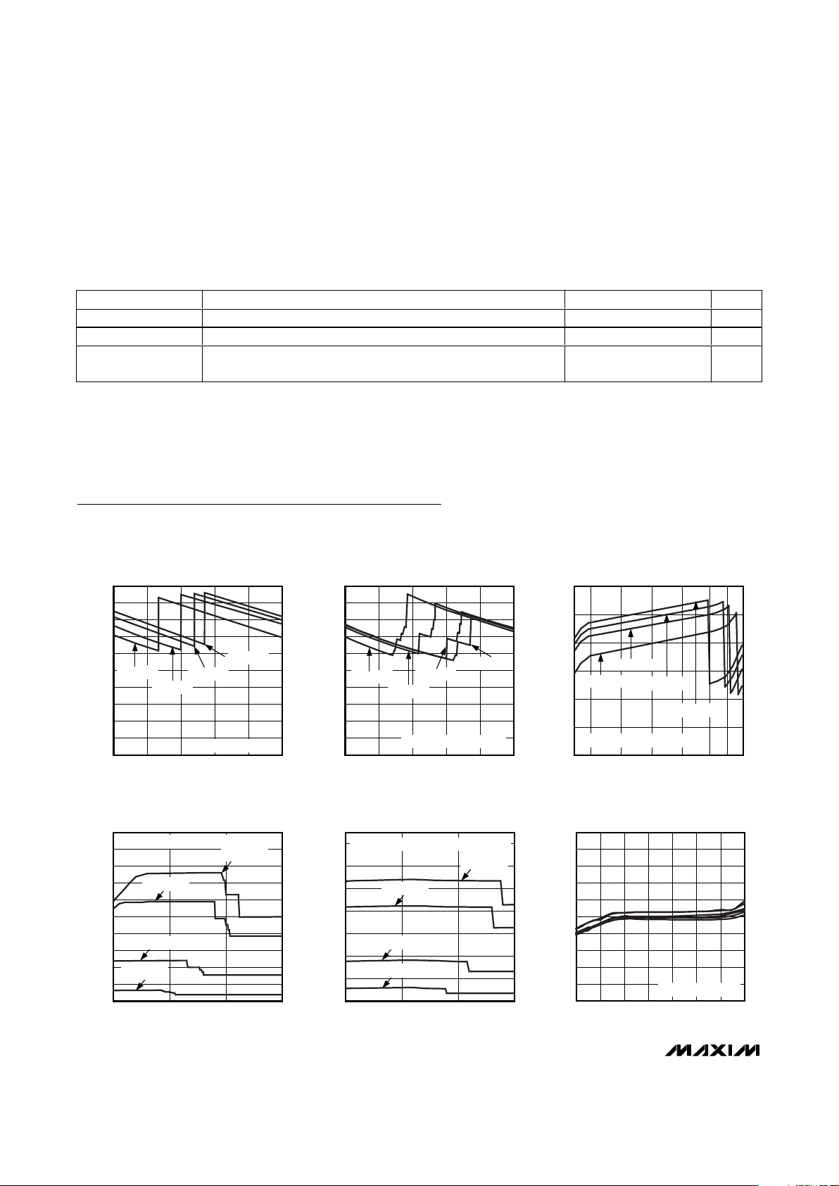
LED CHARGE PUMP
0
30
20
10
40
50
60
70
80
90
100
2.7 3.33.0 3.6 3.9 4.2
EFFICIENCY vs. SUPPLY VOLTAGE
(DRIVING SIX LEDS)
MAX8821 toc01
SUPPLY VOLTAGE (V)
EFFICIENCY (%)
1.6mA/LED
6.4mA/LED
20.8mA/LED
16mA/LED
LEDs HAVE MATCHED V
F
0
30
20
10
40
50
60
70
80
90
100
2.7 3.33.0 3.6 3.9 4.2
EFFICIENCY vs. SUPPLY VOLTAGE
(DRIVING SIX LEDS)
MAX8821 toc02
SUPPLY VOLTAGE (V)
EFFICIENCY (%)
1.6mA/LED
6.4mA/LED
20.8mA/LED
16mA/LED
LEDs HAVE MISMATCHED V
F
20.8mA/LED
40
60
50
80
70
90
100
4.2 3.7 3.63.9 3.8 3.5 3.4 3.0
EFFICIENCY vs. Li+ BATTERY VOLTAGE
DRIVING SIX LEDs
MAX8821 toc03
Li+ BATTERY VOLTAGE (V, TIME-WEIGHTED)
EFFICIENCY P
LED
/P
BATT
(%)
20.8mA/LED
16mA/LED
6.4mA/LED
1.6mA/LED
20.8mA/LEDLEDs HAVE HIGH MATCHED V
F
0
75
50
25
100
125
150
175
200
225
250
2.7 3.2
3.7
4.2
SUPPLY CURRENT
vs. SUPPLY VOLTAGE (DRIVING SIX LEDs)
MAX8821 toc04
SUPPLY VOLTAGE (V)
SUPPLY CURRENT (mA)
I
LED
= 20.8mA
I
LED
= 16mA
I
LED
= 6.4mA
I
LED
= 1.6mA
LEDs HAVE HIGH MISMATCHED V
F
SUPPLY CURRENT
vs. SUPPLY VOLTAGE (RGB MODULE)
MAX8821 toc05
SUPPLY VOLTAGE (V)
SUPPLY CURRENT (mA)
3.73.2
10
20
30
40
50
60
70
0
2.7 4.2
I
LED
= 20.8mA
I
LED
= 16mA
I
LED
= 6.4mA
I
LED
= 1.6mA
RGB MODULE: LUMEX SML-LX3632SISUGSBC
LED CURRENT MATCHING
vs. SUPPLY VOLTAGE (16mA/LED)
MAX8821 toc06
SUPPLY VOLTAGE (V)
LED CURRENT (mA)
5.14.73.9 4.33.53.1
15.6
15.7
15.8
15.9
16.0
16.1
16.2
16.3
16.4
16.5
15.5
2.7 5.5
CHARGE PUMP IN 1.5x
MAX8821
White LED Charge Pump with Mono Class D
Audio Amp and Dual LDO
_______________________________________________________________________________________
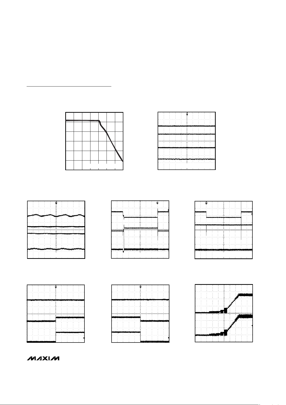
9
Typical Operating Characteristics (continued)
(V
IN1
= V
IN2
= V
IN3
= VDD= 3.6V, V
AGND
= V
PGND1
= V
PGND2
= 0V, circuit of Figure 2, TA= +25°C, unless otherwise noted.)
LED CURRENT vs. AMBIENT
TEMPERATURE
MAX8821 toc07
TEMPERATURE (°C)
LED CURRENT (mA)
806040200-20
5
10
15
20
25
30
0
-40 100
CURRENT DERATING ENABLED
400ns/div
1x MODE OPERATING
WAVEFORMS (V
IN
= 4V)
V
IN
V
NEG
200mA/div
AC-COUPLED
100mV/div
MAX8821 toc08
I
IN
I
LED
ALL LEDs ON, I
LED
= 25.6mA
2V/div
0V
0A
20mA/div
0A
400ns/div
1.5x MODE OPERATING
WAVEFORMS (V
IN
= 3V)
V
IN
V
NEG
200mA/div
AC-COUPLED
100mV/div
MAX8821 toc09
I
IN
I
LED
ALL LEDs ON, I
LED
= 25.6mA
2V/div
0A
20mA/div
0A
0V
1ms/div
LED LINE TRANSIENT WITH MODE CHANGE
(V
IN
= 3.8V TO 3.4V TO 3.8V)
V
IN
200mA/div
3.8V
MAX8821 toc10
I
IN
I
LED6
ALL LEDs AT 25.6mA SETTING
0A
20mA/div
0A
3.4V
1ms/div
LED LINE TRANSIENT WITH MODE CHANGE
(V
IN
= 4.2V TO 3.8V TO 4.2V)
V
IN
200mA/div
4.2V
MAX8821 toc11
I
IN
I
LED6
ALL LEDs AT 25.6mA SETTING
0A
20mA/div
0A
3.8V
1ms/div
LED STARTUP WAVEFORMS
(V
IN
= 4V)
V
IN
50mA/div
AC-COUPLED
50mV/div
MAX8821 toc12
I
IN
I
LED6
0A
20mA/div
0A
1ms/div
LED SHUTDOWN WAVEFORMS
(V
IN
= 4V)
V
IN
50mA/div
AC-COUPLED
MAX8821 toc13
I
IN
I
LED6
0A
20mA/div
0A
50mV/div
400ms/div
LED RAMP-UP
10mA/div
MAX8821 toc14
I
LED6
I
LED5
0A
0A
10mA/div
 Loading...