MAXIM MAX8819A, MAX8819D Technical data
General Description
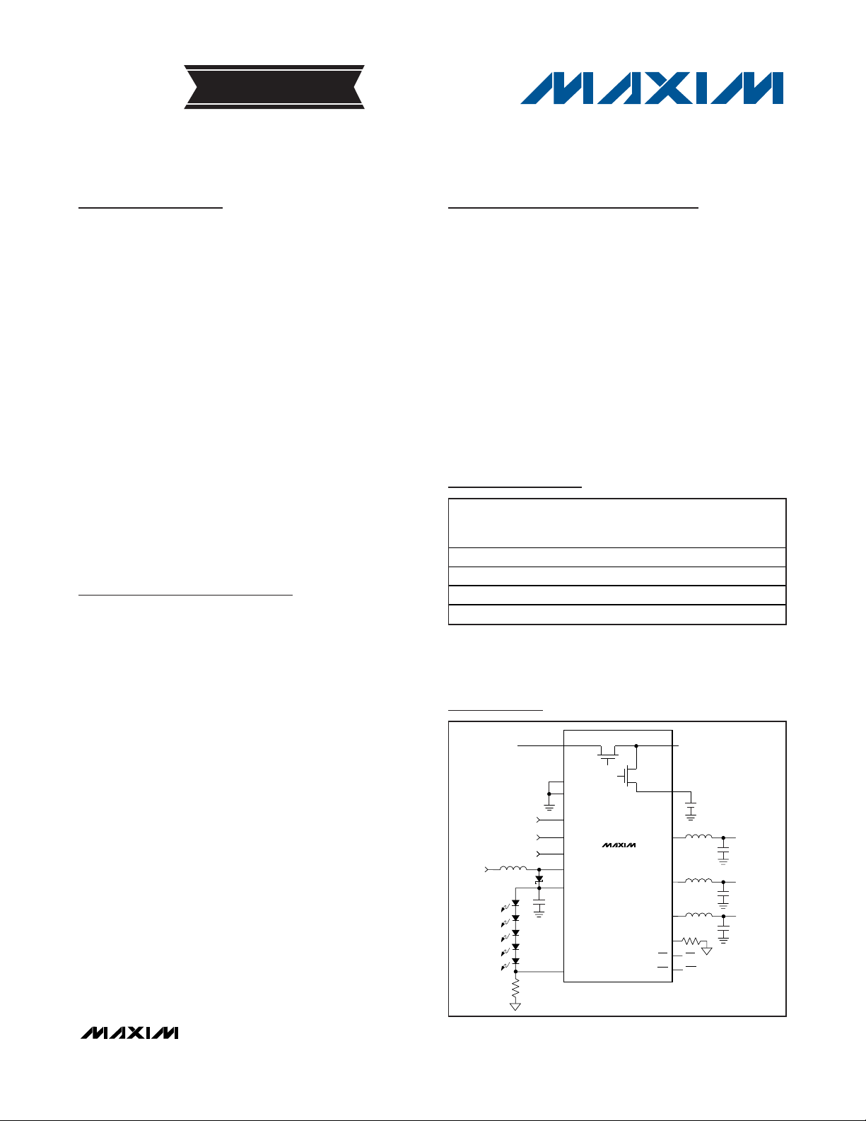
The MAX8819_ is a complete power solution for MP3
players and other handheld applications. The IC
includes a battery charger, step-down converters, and
WLED power. It features an input current-limit switch to
power the IC from an AC-to-DC adapter or USB port, a
1-cell lithium ion (Li+) or lithium polymer (Li-Poly) charger, three step-down converters, and a step-up converter
with serial step dimming for powering two to six white
LEDs. All power switches for charging and switching the
system load between battery and external power are
included on-chip. No external MOSFETs are required.
The MAX8819C/MAX8819D offer a sequenced powerup/power-down of OUT1, OUT2, and then OUT3.
Maxim’s Smart Power Selector™ makes the best use of
AC-to-DC adapter power or limited USB power. Battery
charge current and input current limit are independently set. Input power not used by the system charges the
battery. Charge current is resistor programmable and
the input current limit can be selected as 100mA,
500mA, or 1A. Automatic input selection switches the
system load from battery to external power. In addition,
on-chip thermal limiting reduces the battery charge rate
to prevent charger overheating.
Applications
MP3 Players
Portable GPS Devices
Low-Power Handheld Products
Cellular Telephones
Digital Cameras
Handheld Instrumentation
PDAs
Features
♦ Smart Power Selector
♦ Operates with No Battery Present
♦ USB/AC Adapter One-Cell Li+ Charger
♦ Three 2MHz Step-Down Converters
95% Peak Efficiency
100% Duty Cycle
±3% Output Accuracy over Load/Line/
Temperature
♦ 2 to 6 Series WLED Driver with Dimming Control
♦ RST1 Output
♦ Short-Circuit/Thermal-Overload/Input
Undervoltage/Overvoltage Protection
♦ Power-Up Sequencing (MAX8819C/MAX8819D)
♦ Total Solution Size: Less Than 90mm
2
MAX8819A–MAX8819D
PMIC with Integrated Chargers and Smart
Power Selector in a 4mm x 4mm TQFN
________________________________________________________________
Maxim Integrated Products
1
19-4166; Rev 0; 6/08
For pricing, delivery, and ordering information, please contact Maxim Direct at 1-888-629-4642,
or visit Maxim’s website at www.maxim-ic.com.
Pin Configuration appears at end of data sheet.
Smart Power Selector is a trademark of Maxim Integrated
Products, Inc.
USB/AC-TO-DC
ADAPTER
ENABLE SYSTEM
ENABLE CHARGER
ENABLE BACKLIGHT
SYS
DC
DLIM1
DLIM2
EN123
CEN
EN4
LX4
OVP4
FB4
LX3
LX2
CISET
BAT
SYS
Li+/Li-Poly
BATTERY
OUT1
I/O
OUT2
MEMORY
OUT3
CORE
CHG CHG
LX1
RST1
RST1
MAX8819_
+
Typical Operating Circuit
Ordering Information
+
Denotes a lead-free/RoHS-compliant package.
*
Future product—contact factory for availability.
**
EP = Exposed pad.
PART
TEMP RANGE
PINPACKAGE
SYS
VOLTAGE
(V)
MAX8819AETI+
4.35
MAX8819BETI+
5.3
MAX8819CETI+
4.35
MAX8819DETI+
5.3
EVALUATION KIT
AVAILABLE
-40°C to +85°C 28 TQFN-EP**
-40°C to +85°C 28 TQFN-EP**
-40°C to +85°C 28 TQFN-EP**
-40°C to +85°C 28 TQFN-EP**
MAX8819A–MAX8819D
PMIC with Integrated Chargers and Smart
Power Selector in a 4mm x 4mm TQFN
2 _______________________________________________________________________________________
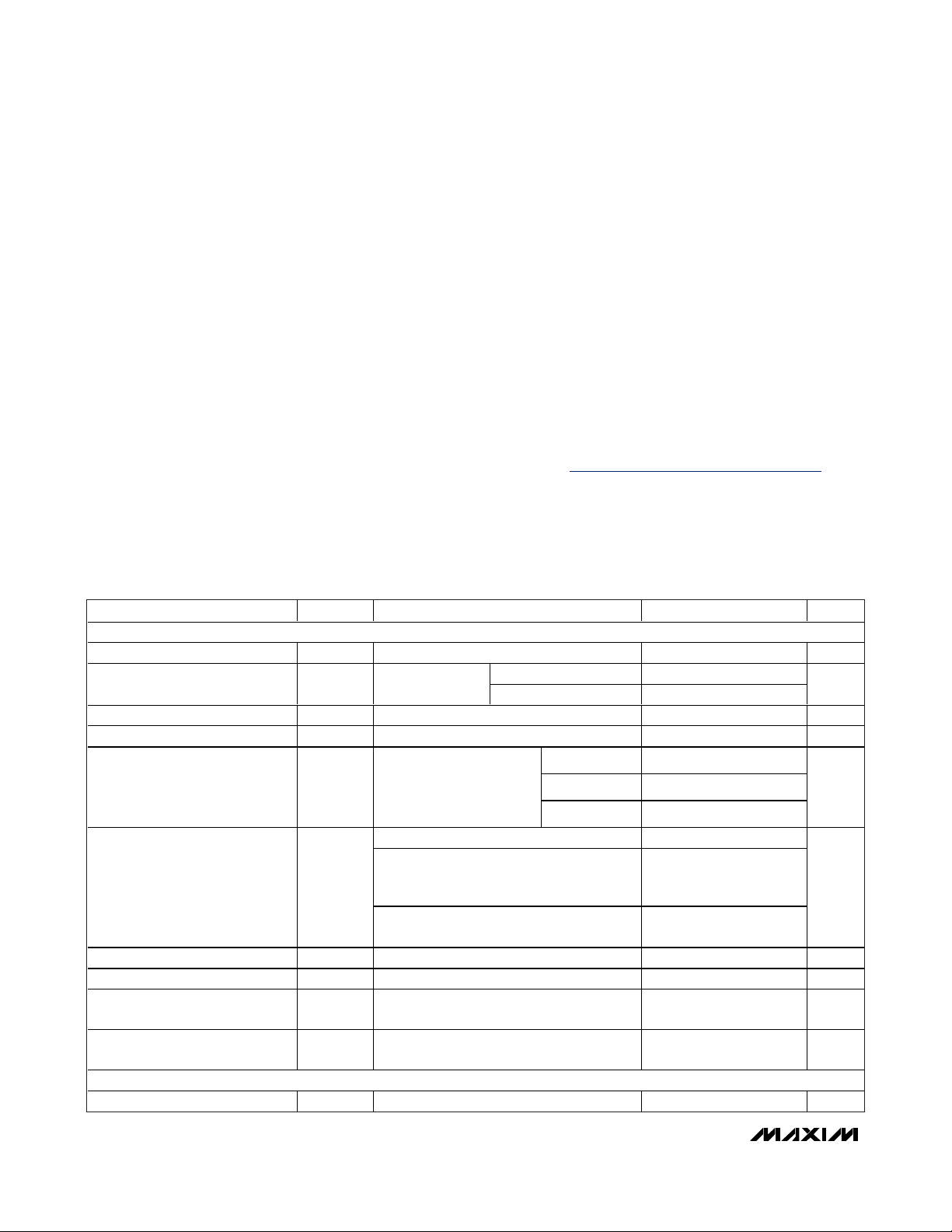
ELECTRICAL CHARACTERISTICS
(DC, LX_ unconnected; VEP= V
GND
= 0V, V
BAT
= 4V, DLIM[1:2] = 00, EN123 = EN4 = low, V
FB1
= V
FB2
= V
FB3
= 1.1V, V
FB4
= 0.6V,
PV13 = PV2 = SYS, T
A
= -40°C to +85°C, capacitors as shown in Figure 1, R
CISET
= 3kΩ, unless otherwise noted.) (Note 3)
Stresses beyond those listed under “Absolute Maximum Ratings” may cause permanent damage to the device. These are stress ratings only, and functional
operation of the device at these or any other conditions beyond those indicated in the operational sections of the specifications is not implied. Exposure to
absolute maximum rating conditions for extended periods may affect device reliability.
ABSOLUTE MAXIMUM RATINGS
DC, SYS, BAT, CISET, DLIM1, DLIM2, EN123
CEN, EN4, CHG, RST1, FB1, FB2, FB3 to GND....-0.3V to +6V
PV2 to GND...............................................-0.3V to (V
SYS
+ 0.3V)
PV13 to SYS...........................................................-0.3V to +0.3V
PG1, PG2, PG3, PG4 to GND................................-0.3V to +0.3V
COMP4, FB4 to GND ................................-0.3V to (V
SYS
+ 0.3V)
LX4 to PG4 .............................................................-0.3V to +33V
OVP4 to GND .........................................................-0.3V to +33V
LX1, LX2, LX3 Continuous Current (Note 1) .........................1.5A
LX4 Current ................................................................750mA
RMS
Output Short-Circuit Duration.....................................Continuous
Continuous Power Dissipation (T
A
= +70°C)
28-Pin Thin QFN Single-Layer Board (derate 20.8mW/°C
above +70°C)...........................................................1666.7mW
28-Pin Thin QFN Multilayer Board (derate 28.6mW/°C
above +70°C)...........................................................2285.7mW
Junction-to-Case Thermal Resistance (θ
JC
) (Note 2)
28-Lead Thin QFN...........................................................3°C/W
Operating Temperature Range ...........................-40°C to +85°C
Junction Temperature........................................-40°C to +125°C
Storage Temperature.........................................-65°C to +150°C
Lead Temperature (soldering, 10s) .................................+300°C
Note 1: LX1, LX2, LX3 have clamp diodes to their respective PG_ and PV_. Applications that forward bias these diodes must take
care not to exceed the package power dissipation limits.
Note 2: Package thermal resistances were obtained using the method described in JEDEC specification JESD51-7, using a four-layer
board. For detailed information on package thermal considerations, refer to http://www.maxim-ic.com/thermal-tutorial
.
PARAMETER SYMBOL CONDITIONS MIN TYP MAX UNITS
DC POWER INPUT
DC Voltage Range V
SYS Regulation Voltage V
DC Undervoltage Threshold V
DC Overvoltage Threshold V
DC Current Limit
(Note 4)
DC Quiescent Current I
DC-to-SYS Dropout Resistance R
DC-to-SYS Soft-Start Time t
DC Thermal-Limit Temperature
DC Thermal-Limit Gain
SYSTEM
System Operating Voltage Range V
DC
SYS_REGVDC
UVLO_DCVDC
OVLO_DCVDC
VDC = 5.75V, V
I
DCLIM
DCIQ
SS-D-S
SYS
for MAX8819B/MAX8819D
or V
MAX8819A/MAX8819C
DLIM[1:2] = 11 (suspend) 0.02 0.035
DLIM[1:2] ≠ 11, I
EN123 = low, EN4 = low, CEN = high,
V
DC
DLIM[1:2] ≠ 11, I
EN4 = low, CEN = low, V
VDC = 4V, I
DS
Die temperature where current limit is
reduced
Amount of input current reduction above
thermal-limit temperature
= 5.75V
rising, 500mV typical hysteresis 3.95 4.00 4.05 V
rising, 300mV typical hysteresis 5.811 5.9 6.000 V
= 4V for
SYS
= 5.5V
MAX8819A/MAX8819C 4.3 4.35 4.4
MAX8819B/MAX8819D 5.1 5.3 5.5
= 5V
SYS
= 0mA, I
SYS
= 0mA, EN123 = low,
SYS
= 400mA, DLIM[1:2] = 01 0.330 0.700 Ω
SYS
DLIM[1:2] = 10 90 95 100
DLIM[1:2] = 01 450 475 500
DLIM[1:2] = 00 900 1000 1100
= 0mA,
BAT
= 5.5V
DC
4.1 5.5 V
2.6 5.5 V
1.33
0.95
1.5 ms
100 °C
5%/°C
V
mA
mA
MAX8819A–MAX8819D
PMIC with Integrated Chargers and Smart
Power Selector in a 4mm x 4mm TQFN
_______________________________________________________________________________________ 3
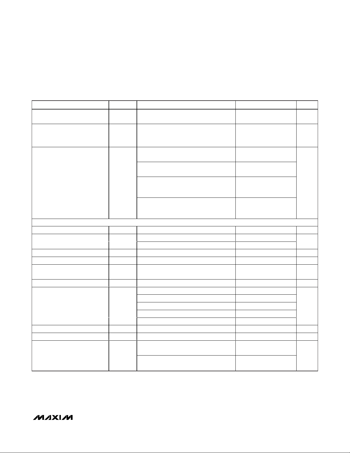
ELECTRICAL CHARACTERISTICS (continued)
(DC, LX_ unconnected; VEP= V
GND
= 0V, V
BAT
= 4V, DLIM[1:2] = 00, EN123 = EN4 = low, V
FB1
= V
FB2
= V
FB3
= 1.1V, V
FB4
= 0.6V,
PV13 = PV2 = SYS, T
A
= -40°C to +85°C, capacitors as shown in Figure 1, R
CISET
= 3kΩ, unless otherwise noted.) (Note 3)
PARAMETER SYMBOL CONDITIONS MIN TYP MAX UNITS
System Undervoltage Lockout
Threshold
BAT-to-SYS Reverse Regulation
Voltage
Quiescent Current IPV+I
BATTERY CHARGER (VDC = 5.0V)
BAT-to-SYS On-Resistance R
BAT Regulation Voltage
(Figure 2)
BAT Recharge Threshold (Note 4) -135 -100 -65 mV
BAT Prequalification Threshold V
R
Resistance Range
CISET
CISET Voltage V
BAT Fast-Charge Current Limit
BAT Prequalification Current V
Top-Off Threshold (Note 5) TA = +25°C, R
BAT Leakage Current
V
V
UVLO_SYSVSYS
DC and BAT are delivering current to SYS;
V
BSRED
I
BAT
MAX8819A/MAX8819C (only)
VDC = 0V, EN123 = low, EN4 = low,
V
BAT
VDC = 5V, DLIM[1:2] = 11, EN123 = low,
EN4 = low, V
VDC = 0V, EN123 = high, EN4 = low,
SYS
V
BAT
dropout)
VDC = 0V, EN123 = high, EN4 = high,
V
BAT
dropout)
BS
BATREG
BATPRQVBAT
VDC = 0V, V
TA = +25°C 4.174 4.200 4.221
TA = -40°C to +85°C 4.158 4.200 4.242
Guaranteed by BAT fast-charge current
limit
CISET
R
CISET
DLIM[1:2] = 10, R
DLIM[1:2] = 01, R
DLIM[1:2] = 00, R
DLIM[1:2] = 00, R
DLIM[1:2] = 00, R
BAT
VDC = 0V, EN123 = low, EN4 = low,
CEN = low, V
V
DC
EN4 = low, V
falling, 100mV hysteresis 2.45 2.5 2.55 V
= 95mA; V
= 4V
= 4V (step-down converters are not in
= 4V (step-down converters are not in
DC
BAT
BAT
= 4.3V,
= 4V
= 4.2V, I
50 66 90 mV
10 20
010
128 290
362 730
= 0.9A 0.073 0.165 Ω
SYS
rising, 180mV hysteresis, Figure 2 2.9 3.0 3.1 V
315kΩ
= 7.5kΩ, I
= 2.5V, R
= 5V, DLIM[1:2] = 11, EN123 = low,
= 267mA 0.9 1.0 1.1 V
BAT
= 3kΩ 87 92 100
CISET
= 3kΩ 450 472 500
CISET
= 15kΩ 170 200 230
CISET
= 7.5kΩ 375 400 425
CISET
= 3.74kΩ 740 802 860
CISET
= 3.74kΩ 60 82 105 mA
CISET
= 3.74kΩ 60 82 105 mA
CISET
BAT
BAT
= 4V
= 4V
10 20
0
μA
V
mA
μA
MAX8819A–MAX8819D
PMIC with Integrated Chargers and Smart
Power Selector in a 4mm x 4mm TQFN
4 _______________________________________________________________________________________
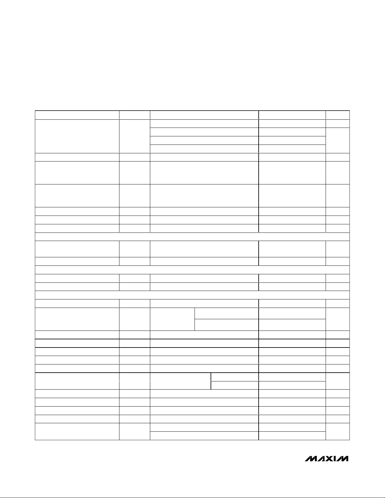
ELECTRICAL CHARACTERISTICS (continued)
(DC, LX_ unconnected; VEP= V
GND
= 0V, V
BAT
= 4V, DLIM[1:2] = 00, EN123 = EN4 = low, V
FB1
= V
FB2
= V
FB3
= 1.1V, V
FB4
= 0.6V,
PV13 = PV2 = SYS, T
A
= -40°C to +85°C, capacitors as shown in Figure 1, R
CISET
= 3kΩ, unless otherwise noted.) (Note 3)
PARAMETER SYMBOL CONDITIONS MIN TYP MAX UNITS
Charger Soft-Start Time t
Timer Accuracy +15 %
Timer Suspend Threshold
Timer Extend Threshold
Prequalification Time t
Fast-Charge Time t
Top-Off Time t
POWER SEQUENCING (Figures 6 and 7)
REG1, REG2, REG3 Soft-Start
Time
REG4 Soft-Start Time t
REGULATOR THERMAL SHUTDOWN
Thermal Shutdown Temperature TJ rising +165 °C
Thermal Shutdown Hysteresis 15 °C
REG1–SYNCHRONOUS STEP-DOWN CONVERTER
Input Voltage PV13 supplied from SYS V
Maximum Output Current
Short-Circuit Current L = 4.7μH, R
Short-Circuit Detection Threshold 230 mV
Short-Circuit Foldback Frequency f
FB1 Voltage (Note 7) 0.997 1.01 1.028 V
Output Voltage Range 1V
FB1 Leakage Current V
Load Regulation I
Line Regulation (Note 9) 1 %/D
p-Channel On-Resistance V
n-Channel On-Resistance V
p-Channel Current-Limit
Threshold
SS_CHG
t
SS1
t
SS3
SS4
PQ
FC
TO
, t
Slew rate 333 mA/ms
Time from 0 to 500mA 1.5
Time from 0 to 100mA 0.3
Time from 100mA to 500mA 1.2
CISET voltage when the fast-charge timer
suspends; 300mV translates to 20% of the
maximum fast-charge current limit
CISET voltage when the fast-charge timer
extends; 750mV translates to 50% of the
maximum fast-charge current limit
,
SS2
C
L = 4.7μH,
R
(Note 6)
MAX8819A/MAX8819B 0.565 0.600 0.640
MAX8819C/MAX8819D 0.615 0.650 0.750
= 0.022μF to GND 5 ms
COMP4
= 0.13Ω
LSR
= 0.13Ω 600 mA
LSR
= 1.01V
FB1
= 100mA to 300mA 1 %
OUT1
= 4.0V, I
PV13
PV13
= 4.0V, I
LX1
LX1
MAX8819A/MAX8819B 400
MAX8819C/MAX8819D 550
TA = +25°C -50 -5 +50
T
A
= 180mA 190 mΩ
= 180mA 250 mΩ
250 300 350 mV
700 750 800 mV
33 min
660 min
33 min
2.6 ms
SYS
/3 Hz
OSC
= +85°C -10
SYS
ms
V
mA
V
nA
A
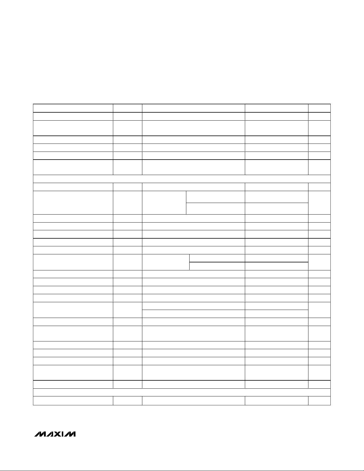
MAX8819A–MAX8819D
ELECTRICAL CHARACTERISTICS (continued)
(DC, LX_ unconnected; VEP= V
GND
= 0V, V
BAT
= 4V, DLIM[1:2] = 00, EN123 = EN4 = low, V
FB1
= V
FB2
= V
FB3
= 1.1V, V
FB4
= 0.6V,
PV13 = PV2 = SYS, T
A
= -40°C to +85°C, capacitors as shown in Figure 1, R
CISET
= 3kΩ, unless otherwise noted.) (Note 3)
PMIC with Integrated Chargers and Smart
Power Selector in a 4mm x 4mm TQFN
_______________________________________________________________________________________ 5
PARAMETER SYMBOL CONDITIONS MIN TYP MAX UNITS
Skip-Mode Transition Current (Note 8) 80 mA
n-Channel Zero-Crossing
Threshold
Maximum Duty Cycle 100 %
Minimum Duty Cycle 12.5 %
PWM Frequency f
Internal Discharge Resistance in
Shutdown
REG2–SYNCHRONOUS STEP-DOWN CONVERTER
Input Voltage PV2 supplied from SYS V
Maximum Output Current
Short-Circuit Current L = 4.7μH, R
Short-Circuit Detection Threshold 230 mV
Short-Circuit Foldback Frequency f
FB2 Voltage (Note 7) 0.997 1.012 1.028 V
Output Voltage Range 1V
FB2 Leakage Current V
Load Regulation I
Line Regulation (Note 9) 1 %/D
p-Channel On-Resistance V
n-Channel On-Resistance V
p-Channel Current-Limit
Threshold
Skip-Mode Transition Current (Note 8) 80 mA
n-Channel Zero-Crossing
Threshold
Maximum Duty Cycle 100 %
Minimum Duty Cycle 12.5 %
PWM Frequency f
Internal Discharge Resistance in
Shutdown
REG2 Disable ΔI
REG3–SYNCHRONOUS STEP-DOWN CONVERTER
Input Voltage PV13 supplied from SYS V
OSC
OSC
SYS
EN123 = low, resistance from LX1 to PG1 1.0 kΩ
L = 4.7μH,
= 0.13Ω
R
LSR
(Note 6)
= 0.13Ω 600 mA
LSR
= 1.01V
FB2
= 100mA to 300mA 1 %
OUT2
= 4.0V, I
PV2
= 4.0V, I
PV2
MAX8819A/MAX8819B 0.512 0.550 0.595
MAX8819C/MAX8819D 0.565 0.600 0.700
EN123 = low, resistance from LX2 to PG2 1.0 kΩ
V
= 0V, REG2 disabled (Note 10) -25 μA
PV2
= 180mA 290 mΩ
LX2
= 180mA 200 mΩ
LX2
MAX8819A/MAX8819B 300
MAX8819C/MAX8819D 500
TA = +25°C -50 -5 +50
= +85°C -50
T
A
1.8 2.0 2.2 MHz
1.8 2.0 2.2 MHz
10 mA
SYS
/3 Hz
OSC
SYS
10 mA
SYS
mA
nA
V
V
A
V
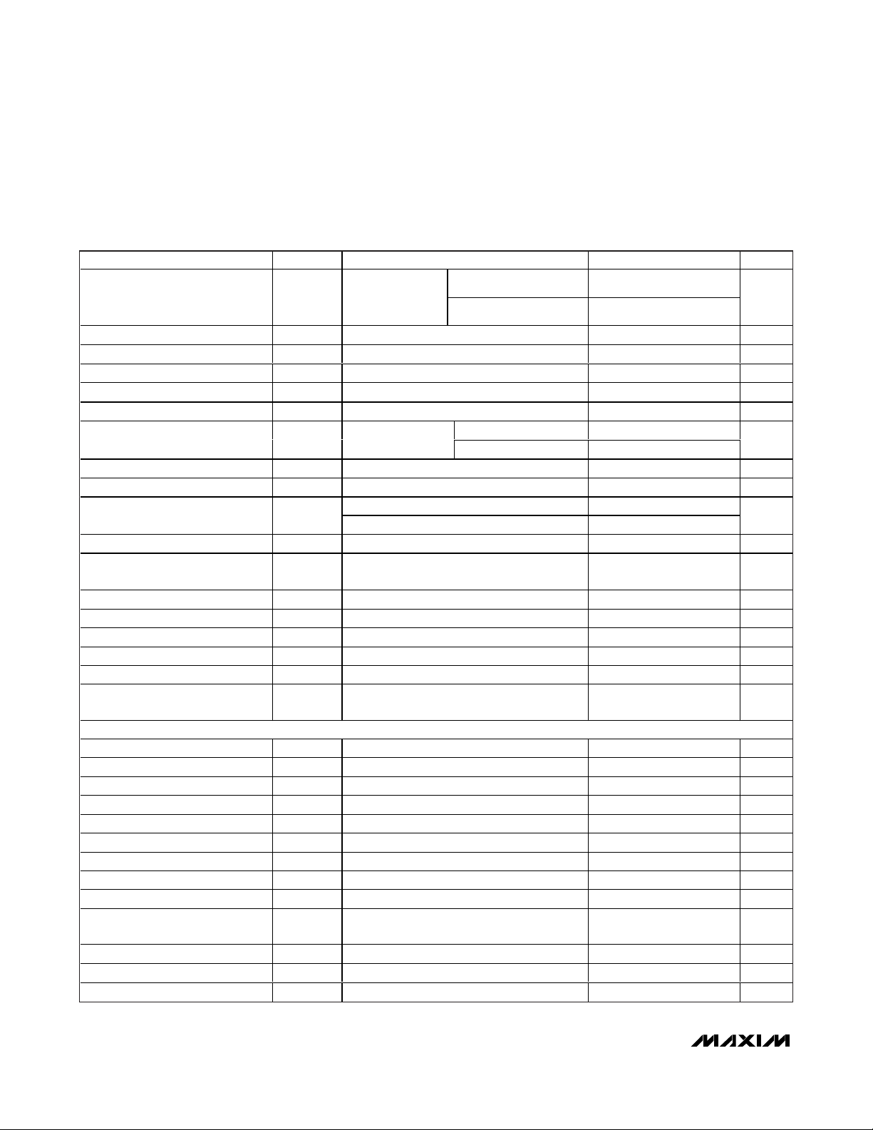
MAX8819A–MAX8819D
PMIC with Integrated Chargers and Smart
Power Selector in a 4mm x 4mm TQFN
6 _______________________________________________________________________________________
ELECTRICAL CHARACTERISTICS (continued)
(DC, LX_ unconnected; VEP= V
GND
= 0V, V
BAT
= 4V, DLIM[1:2] = 00, EN123 = EN4 = low, V
FB1
= V
FB2
= V
FB3
= 1.1V, V
FB4
= 0.6V,
PV13 = PV2 = SYS, T
A
= -40°C to +85°C, capacitors as shown in Figure 1, R
CISET
= 3kΩ, unless otherwise noted.) (Note 3)
Maximum Output Current
Short-Circuit Current L = 4.7μH, R
Short-Circuit Detection Threshold 230 mV
Short-Circuit Foldback Frequency f
FB3 Voltage (Note 7) 0.997 1.01 1.028 V
Output Voltage Range 1V
FB3 Leakage Current V
Load Regulation I
Line Regulation (Note 9) 1 %/D
p-Channel Current-Limit
Threshold
Skip-Mode Transition Current (Note 8) 80 mA
n-Channel Zero-Crossing
Threshold
p-Channel On-Resistance V
n-Channel On-Resistance V
Maximum Duty Cycle 100 %
Minimum Duty Cycle 12.5 %
PWM Frequency f
Internal Discharge Resistance in
Shutdown
REG4–STEP-UP CONVERTER
Input Voltage Power supplied from SYS (see Figure 1) 2.4 5.5 V
Output Voltage Range V
FB4 Regulation Voltage V
FB4 Leakage REG4 disabled (EN4 = low) -0.050 +0.005 +0.050 μA
Switching Frequency 0.9 1 1.1 MHz
Minimum Duty Cycle 5%
Maximum Duty Cycle 90 94 %
OVP4 Overvoltage Detection
OVP4 Input Current OVP4 = SYS, EN4 = high 4 μA
OVP4 Leakage Current
n-Channel On-Resistance V
n-Channel Off-Leakage Current V
n-Channel Current Limit 555 695 950 mA
PARAMETER SYMBOL CONDITIONS MIN TYP MAX UNITS
OSC
OUT4
V
FB4
OVP
L = 4.7μH,
= 0.13Ω
R
LSR
(Note 6)
= 0.13Ω 600 mA
LSR
= 1.01V
FB3
= 100mA to 300mA 1.3 %
OUT3
MAX8819A/MAX8819B 0.512 0.550 0.595
MAX8819C/MAX8819D 0.565 0.600 0.700
= 4.0V, I
PV13
= 4.0V, I
PV13
EN123 = low, resistance from LX3 to PG3 1.0 kΩ
No dimming 475 500 525 mV
REG4 disabled (EN4 = low),
OVP4 = SYS
= 4.0V, I
SYS
= 28V -1 +0.001 +1 μA
LX4
LX3
LX3
= 200mA 395 mΩ
LX4
MAX8819A/MAX8819B 300
MAX8819C/MAX8819D 500
TA = +25°C -50 -5 +50
T
= +85°C -50
A
= 180mA 290 mΩ
= 180mA 120 mΩ
1.8 2.0 2.2 MHz
V
SYS
24 25 26 V
-1 +0.001 +1 μA
/3 Hz
OSC
SYS
10 mA
24 V
mA
V
nA
A
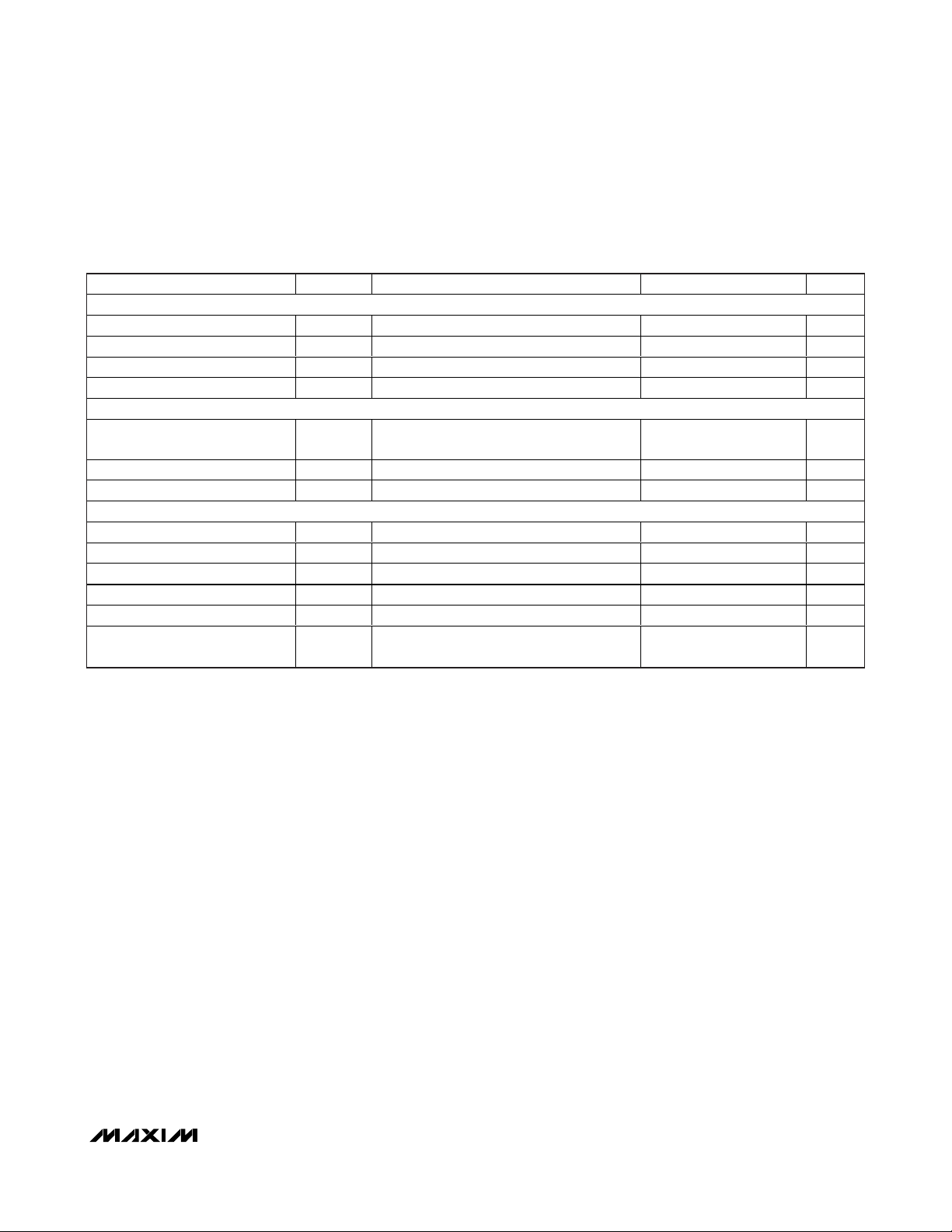
MAX8819A–MAX8819D
PMIC with Integrated Chargers and Smart
Power Selector in a 4mm x 4mm TQFN
_______________________________________________________________________________________ 7
ELECTRICAL CHARACTERISTICS (continued)
(DC, LX_ unconnected; VEP= V
GND
= 0V, V
BAT
= 4V, DLIM[1:2] = 00, EN123 = EN4 = low, V
FB1
= V
FB2
= V
FB3
= 1.1V, V
FB4
= 0.6V,
PV13 = PV2 = SYS, T
A
= -40°C to +85°C, capacitors as shown in Figure 1, R
CISET
= 3kΩ, unless otherwise noted.) (Note 3)
Note 3: Limits are 100% production tested at TA= +25°C. Limits over the operating temperature range are guaranteed through cor-
relation using statistical quality control (SQC) methods.
Note 4: The charger transitions from done to fast-charge mode at this BAT recharge threshold.
Note 5: The charger transitions from fast-charge to top-off mode at this top-off threshold (Figure 2).
Note 6: The maximum output current is guaranteed by correlation to the p-channel current-limit threshold, p-channel on-resistance,
n-channel on-resistance, oscillator frequency, input voltage range, and output voltage range. The parameter is stated for
a 4.7μH inductor with 0.13Ω series resistance. See the
Step-Down Converter Maximum Output Current
section for more
information.
Note 7: The step-down output voltages are 1% high with no load due to the load-line architecture.
Note 8: The skip-mode current threshold is the transition point between fixed-frequency PWM operation and skip-mode operation.
The specification is given in terms of output load current for inductor values shown in the typical application circuit (Figure 1).
Note 9: Line regulation for the step-down converters is measured as ΔV
OUT
/ΔD, where D is the duty cycle (approximately
V
OUT/VIN
).
Note 10: REG2 is disabled by connecting PV2 to ground, decreasing the quiescent current.
PARAMETER SYMBOL CONDITIONS MIN TYP MAX UNITS
LED DIMMING CONTROL (EN4)
EN4 Low Shutdown Delay t
EN4 High Enable Delay (Figure 8) t
EN4 Low Time t
EN4 High Time t
RESET (RST)
Reset Trip Threshold V
Reset Deassert Delay Time t
Reset Glitch Filter t
LOGIC (DLIM1, DLIM2, EN123, EN4, CHG, RST1)
Logic Input-Voltage Low VDC = 4.1V to 5.5V, V
Logic Input-Voltage High VDC = 4.1V to 5.5V, V
Logic Input Pulldown Resistance V
Logic Leakage Current V
Logic Output Voltage Low I
Logic Output-High Leakage
Current
SHDN
H_INIT
THRST
DRST
GLRST
LO
HI
Voltage from FB1 to GND, V
50mV hysteresis
= 0.4V to 5.5V, CEN, EN123, EN4 400 760 1200 kΩ
LOGIC
= 0 to 5.5V, DLIM1, DLIM2 -1.0 +0.001 +1.0 μA
LOGIC
= 1mA 7 15 mV
SINK
V
= 5.5V -1.0 +0.001 +1.0 μA
LOGIC
falling,
FB1
= 2.6V to 5.5V 0.4 V
SYS
= 2.6V to 5.5V 1.2 V
SYS
100 μs
0.5 500 μs
0.5 μs
0.765 0.858 0.945 V
180 200 220 ms
2 3.2 ms
50 μs
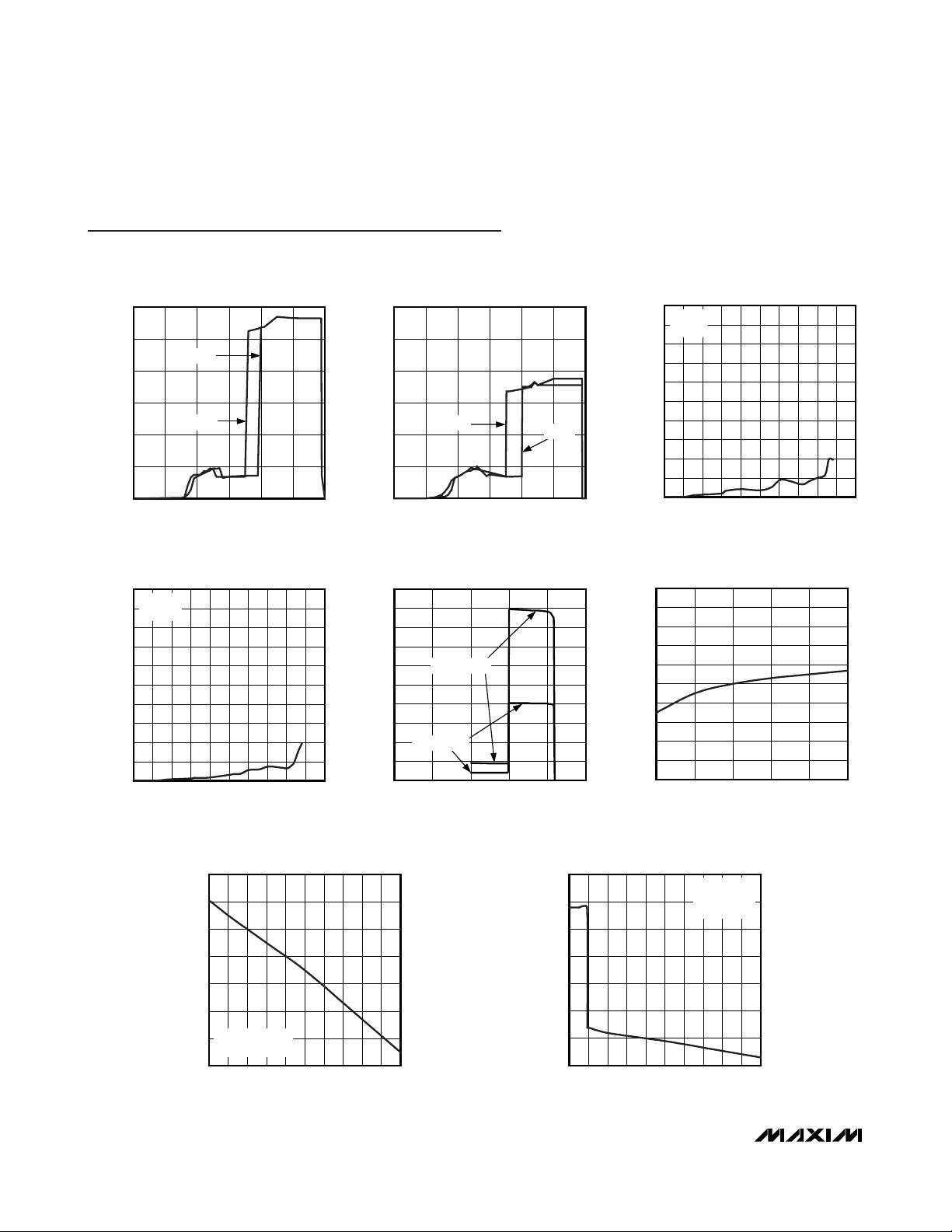
MAX8819A–MAX8819D
PMIC with Integrated Chargers and Smart
Power Selector in a 4mm x 4mm TQFN
8 _______________________________________________________________________________________
Typical Operating Characteristics
(TA = +25°C, unless otherwise noted.)
BATTERY LEAKAGE CURRENT
vs. BATTERY VOLTAGE
BATTERY VOLTAGE (V)
BATTERY LEAKAGE CURRENT (nA)
MAX8819A toc04
0 0.5 1.0 1.5 2.0 2.5 3.0 3.5 4.0 4.5 5.0
0
100
200
300
400
500
600
700
800
900
1000
VDC = 0V
EN123 = 1
CHARGE CURRENT
vs. BATTERY VOLTAGE
BATTERY VOLTAGE (V)
CHARGE CURRENT (mA)
MAX8819A toc05
034215
0
50
100
150
200
250
300
350
400
450
500
R
CISET
= 6.8kΩ
R
CISET
= 15kΩ
BATTERY REGULATION VOLTAGE
vs. TEMPERATURE
TEMPERATURE (°C)
BATTERY REGULATION VOLTAGE (V)
MAX8819A toc06
-40 -15 10 35 60 85
4.15
4.16
4.17
4.18
4.19
4.20
4.21
4.22
4.23
4.24
4.25
SYSTEM VOLTAGE
vs. SYSTEM CURRENT
OUTPUT CURRENT (mA)
SYSTEM VOLTAGE (V)
MAX8819A toc07
0 100 200 300 400 500 600 700 800 900 1000
3.88
3.90
3.92
3.94
3.96
3.98
4.00
4.02
DC UNCONNECTED
V
BATT
= 4V
SYSTEM VOLTAGE
vs. SYSTEM CURRENT
OUTPUT CURRENT (mA)
SYSTEM VOLTAGE (V)
MAX8819A toc08
0 100 200 300 400 500 600 700 800 900 1000
3.8
3.9
4.0
4.1
4.2
4.3
4.4
4.5
VDC = 5.1V
V
BATT
= 4V
DLIM[1:2] = 10
QUIESCENT CURRENT vs.
SUPPLY VOLTAGE (CHARGER ENABLED)
1.2
1.0
0.8
0.6
0.4
QUIESCENT CURRENT (mA)
0.2
0
0123456
RISING
FALLING
SUPPLY VOLTAGE (V)
1.2
1.0
MAX8819A toc01
0.8
0.6
0.4
QUIESCENT CURRENT (mA)
0.2
0
0123456
QUIESCENT CURRENT vs. VDC
CHARGER DISABLED
FALLING
DC VOLTAGE, VDC (V)
RISING
1000
900
MAX8819A toc02
800
700
600
500
400
300
200
BATTERY LEAKAGE CURRENT (nA)
100
BATTERY LEAKAGE CURRENT
vs. BATTERY VOLTAGE
VDC = 5V
EN123 = 1
0
0 0.5 1.0 1.5 2.0 2.5 3.0 3.5 4.0 4.5 5.0
MAX8819A toc03
BATTERY VOLTAGE (V)
MAX8819A–MAX8819D
PMIC with Integrated Chargers and Smart
Power Selector in a 4mm x 4mm TQFN
_______________________________________________________________________________________ 9
Typical Operating Characteristics (continued)
(TA = +25°C, unless otherwise noted.)
SYSTEM VOLTAGE
vs. SYSTEM CURRENT
4.5
4.4
4.3
4.2
4.1
SYSTEM VOLTAGE (V)
4.0
VDC = 5.1V
3.9
3.8
= 4V
V
BATT
DLIM[1:2] = 01
0 100 200 300 400 500 600 700 800 900 1000
OUTPUT CURRENT (mA)
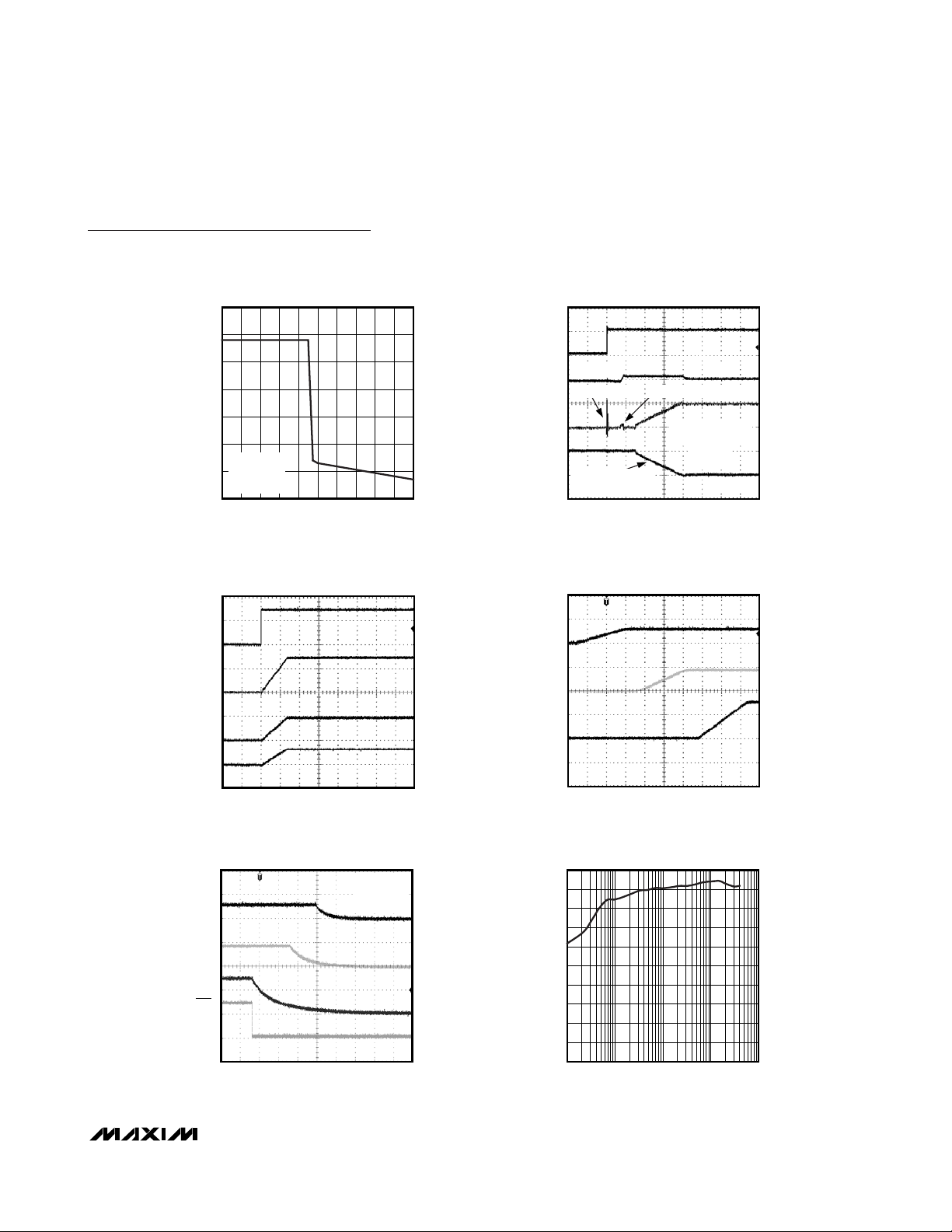
POWER-UP SEQUENCING
(MAX8819A/MAX8819B)
V
EN123
V
V1
MAX8819A toc11
MAX8819A toc09
2V/div
0V
2V/div
0V
V
DC
V
SYS
I
DC
I
BAT
V
V3
V
V2
AC-TO-DC ADAPTER CONNECT
CHARGING
4.3V
C
SYS
400μs/div
3.84V
C
DC
BATTERY CHARGER
SOFT-START
POWER-UP SEQUENCING
(MAX8819C/MAX8819D)
MAX8819A toc10
4V
CHARGING
NEGATIVE BATTERY
CURRENT FLOWS
INTO THE
BATTERY
1A
-1A
MAX8819A toc12
5V/div
2V/div
1A/div
1A/div
2V/div
0V
2V/div
0V
V
V2
V
V3
2ms/div
POWER-DOWN SEQUENCING
(MAX8819C/MAX8819D)
V
V3
V
V2
V
V1
V
RST1
100μs/div
MAX8819A toc13
IV3 = 200mA
= 180mA
I
V2
= 220mA
I
V1
2V/div
0V
2V/div
0V
2V/div
0V
2V/div
0V
2V/div
0V
2V/div
0V
V
V1
1ms/div
REG1 EFFICIENCY
vs. LOAD CURRENT (V
100
90
80
70
60
50
40
30
REG1 EFFICIENCY (%)
20
10
0
0.1 1 10 100 1000
LOAD CURRENT (mA)
REG1
= 3.01V)
2V/div
0V
MAX8819A toc14
 Loading...