

General Description
The MAX8819_ is a complete power solution for MP3
players and other handheld applications. The IC
includes a battery charger, step-down converters, and
WLED power. It features an input current-limit switch to
power the IC from an AC-to-DC adapter or USB port, a
1-cell lithium ion (Li+) or lithium polymer (Li-Poly) charger, three step-down converters, and a step-up converter
with serial step dimming for powering two to six white
LEDs. All power switches for charging and switching the
system load between battery and external power are
included on-chip. No external MOSFETs are required.
The MAX8819C/MAX8819D offer a sequenced powerup/power-down of OUT1, OUT2, and then OUT3.
Maxim’s Smart Power Selector™ makes the best use of
AC-to-DC adapter power or limited USB power. Battery
charge current and input current limit are independently set. Input power not used by the system charges the
battery. Charge current is resistor programmable and
the input current limit can be selected as 100mA,
500mA, or 1A. Automatic input selection switches the
system load from battery to external power. In addition,
on-chip thermal limiting reduces the battery charge rate
to prevent charger overheating.
Applications
MP3 Players
Portable GPS Devices
Low-Power Handheld Products
Cellular Telephones
Digital Cameras
Handheld Instrumentation
PDAs
Features
♦ Smart Power Selector
♦ Operates with No Battery Present
♦ USB/AC Adapter One-Cell Li+ Charger
♦ Three 2MHz Step-Down Converters
95% Peak Efficiency
100% Duty Cycle
±3% Output Accuracy over Load/Line/
Temperature
♦ 2 to 6 Series WLED Driver with Dimming Control
♦ RST1 Output
♦ Short-Circuit/Thermal-Overload/Input
Undervoltage/Overvoltage Protection
♦ Power-Up Sequencing (MAX8819C/MAX8819D)
♦ Total Solution Size: Less Than 90mm
2
MAX8819A–MAX8819D
PMIC with Integrated Chargers and Smart
Power Selector in a 4mm x 4mm TQFN
________________________________________________________________
Maxim Integrated Products
1
19-4166; Rev 0; 6/08
For pricing, delivery, and ordering information, please contact Maxim Direct at 1-888-629-4642,
or visit Maxim’s website at www.maxim-ic.com.
Pin Configuration appears at end of data sheet.
Smart Power Selector is a trademark of Maxim Integrated
Products, Inc.
USB/AC-TO-DC
ADAPTER
ENABLE SYSTEM
ENABLE CHARGER
ENABLE BACKLIGHT
SYS
DC
DLIM1
DLIM2
EN123
CEN
EN4
LX4
OVP4
FB4
LX3
LX2
CISET
BAT
SYS
Li+/Li-Poly
BATTERY
OUT1
I/O
OUT2
MEMORY
OUT3
CORE
CHG CHG
LX1
RST1
RST1
MAX8819_
+
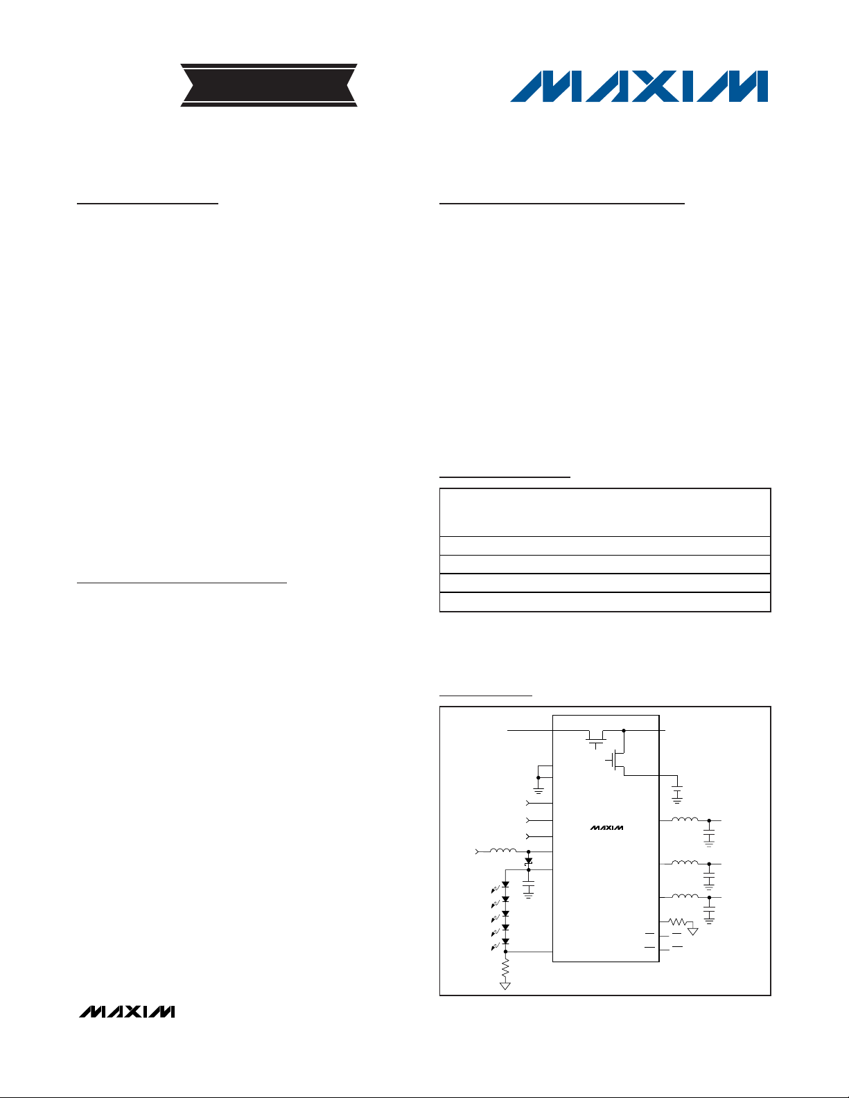
Typical Operating Circuit
Ordering Information
+
Denotes a lead-free/RoHS-compliant package.
*
Future product—contact factory for availability.
**
EP = Exposed pad.
PART
TEMP RANGE
PINPACKAGE
SYS
VOLTAGE
(V)
MAX8819AETI+
4.35
MAX8819BETI+
5.3
MAX8819CETI+
4.35
MAX8819DETI+
5.3
EVALUATION KIT
AVAILABLE
-40°C to +85°C 28 TQFN-EP**
-40°C to +85°C 28 TQFN-EP**
-40°C to +85°C 28 TQFN-EP**
-40°C to +85°C 28 TQFN-EP**
MAX8819A–MAX8819D
PMIC with Integrated Chargers and Smart
Power Selector in a 4mm x 4mm TQFN
2 _______________________________________________________________________________________
ELECTRICAL CHARACTERISTICS
(DC, LX_ unconnected; VEP= V
GND
= 0V, V
BAT
= 4V, DLIM[1:2] = 00, EN123 = EN4 = low, V
FB1
= V
FB2
= V
FB3
= 1.1V, V
FB4
= 0.6V,
PV13 = PV2 = SYS, T
A
= -40°C to +85°C, capacitors as shown in Figure 1, R
CISET
= 3kΩ, unless otherwise noted.) (Note 3)
Stresses beyond those listed under “Absolute Maximum Ratings” may cause permanent damage to the device. These are stress ratings only, and functional
operation of the device at these or any other conditions beyond those indicated in the operational sections of the specifications is not implied. Exposure to
absolute maximum rating conditions for extended periods may affect device reliability.
ABSOLUTE MAXIMUM RATINGS
DC, SYS, BAT, CISET, DLIM1, DLIM2, EN123
CEN, EN4, CHG, RST1, FB1, FB2, FB3 to GND....-0.3V to +6V
PV2 to GND...............................................-0.3V to (V
SYS
+ 0.3V)
PV13 to SYS...........................................................-0.3V to +0.3V
PG1, PG2, PG3, PG4 to GND................................-0.3V to +0.3V
COMP4, FB4 to GND ................................-0.3V to (V
SYS
+ 0.3V)
LX4 to PG4 .............................................................-0.3V to +33V
OVP4 to GND .........................................................-0.3V to +33V
LX1, LX2, LX3 Continuous Current (Note 1) .........................1.5A
LX4 Current ................................................................750mA
RMS
Output Short-Circuit Duration.....................................Continuous
Continuous Power Dissipation (T
A
= +70°C)
28-Pin Thin QFN Single-Layer Board (derate 20.8mW/°C
above +70°C)...........................................................1666.7mW
28-Pin Thin QFN Multilayer Board (derate 28.6mW/°C
above +70°C)...........................................................2285.7mW
Junction-to-Case Thermal Resistance (θ
JC
) (Note 2)
28-Lead Thin QFN...........................................................3°C/W
Operating Temperature Range ...........................-40°C to +85°C
Junction Temperature........................................-40°C to +125°C
Storage Temperature.........................................-65°C to +150°C
Lead Temperature (soldering, 10s) .................................+300°C
Note 1: LX1, LX2, LX3 have clamp diodes to their respective PG_ and PV_. Applications that forward bias these diodes must take
care not to exceed the package power dissipation limits.
Note 2: Package thermal resistances were obtained using the method described in JEDEC specification JESD51-7, using a four-layer
board. For detailed information on package thermal considerations, refer to http://www.maxim-ic.com/thermal-tutorial
.
PARAMETER SYMBOL CONDITIONS MIN TYP MAX UNITS
DC POWER INPUT
DC Voltage Range V
SYS Regulation Voltage V
DC Undervoltage Threshold V
DC Overvoltage Threshold V
DC Current Limit
(Note 4)
DC Quiescent Current I
DC-to-SYS Dropout Resistance R
DC-to-SYS Soft-Start Time t
DC Thermal-Limit Temperature
DC Thermal-Limit Gain
SYSTEM
System Operating Voltage Range V
DC
SYS_REGVDC
UVLO_DCVDC
OVLO_DCVDC
VDC = 5.75V, V
I
DCLIM
DCIQ
SS-D-S
SYS
for MAX8819B/MAX8819D
or V
MAX8819A/MAX8819C
DLIM[1:2] = 11 (suspend) 0.02 0.035
DLIM[1:2] ≠ 11, I
EN123 = low, EN4 = low, CEN = high,
V
DC
DLIM[1:2] ≠ 11, I
EN4 = low, CEN = low, V
VDC = 4V, I
DS
Die temperature where current limit is
reduced
Amount of input current reduction above
thermal-limit temperature
= 5.75V
rising, 500mV typical hysteresis 3.95 4.00 4.05 V
rising, 300mV typical hysteresis 5.811 5.9 6.000 V
= 4V for
SYS
= 5.5V
MAX8819A/MAX8819C 4.3 4.35 4.4
MAX8819B/MAX8819D 5.1 5.3 5.5
= 5V
SYS
= 0mA, I
SYS
= 0mA, EN123 = low,
SYS
= 400mA, DLIM[1:2] = 01 0.330 0.700 Ω
SYS
DLIM[1:2] = 10 90 95 100
DLIM[1:2] = 01 450 475 500
DLIM[1:2] = 00 900 1000 1100
= 0mA,
BAT
= 5.5V
DC
4.1 5.5 V
2.6 5.5 V
1.33
0.95
1.5 ms
100 °C
5%/°C
V
mA
mA
MAX8819A–MAX8819D
PMIC with Integrated Chargers and Smart
Power Selector in a 4mm x 4mm TQFN
_______________________________________________________________________________________ 3
ELECTRICAL CHARACTERISTICS (continued)
(DC, LX_ unconnected; VEP= V
GND
= 0V, V
BAT
= 4V, DLIM[1:2] = 00, EN123 = EN4 = low, V
FB1
= V
FB2
= V
FB3
= 1.1V, V
FB4
= 0.6V,
PV13 = PV2 = SYS, T
A
= -40°C to +85°C, capacitors as shown in Figure 1, R
CISET
= 3kΩ, unless otherwise noted.) (Note 3)
PARAMETER SYMBOL CONDITIONS MIN TYP MAX UNITS
System Undervoltage Lockout
Threshold
BAT-to-SYS Reverse Regulation
Voltage
Quiescent Current IPV+I
BATTERY CHARGER (VDC = 5.0V)
BAT-to-SYS On-Resistance R
BAT Regulation Voltage
(Figure 2)
BAT Recharge Threshold (Note 4) -135 -100 -65 mV
BAT Prequalification Threshold V
R
Resistance Range
CISET
CISET Voltage V
BAT Fast-Charge Current Limit
BAT Prequalification Current V
Top-Off Threshold (Note 5) TA = +25°C, R
BAT Leakage Current
V
V
UVLO_SYSVSYS
DC and BAT are delivering current to SYS;
V
BSRED
I
BAT
MAX8819A/MAX8819C (only)
VDC = 0V, EN123 = low, EN4 = low,
V
BAT
VDC = 5V, DLIM[1:2] = 11, EN123 = low,
EN4 = low, V
VDC = 0V, EN123 = high, EN4 = low,
SYS
V
BAT
dropout)
VDC = 0V, EN123 = high, EN4 = high,
V
BAT
dropout)
BS
BATREG
BATPRQVBAT
VDC = 0V, V
TA = +25°C 4.174 4.200 4.221
TA = -40°C to +85°C 4.158 4.200 4.242
Guaranteed by BAT fast-charge current
limit
CISET
R
CISET
DLIM[1:2] = 10, R
DLIM[1:2] = 01, R
DLIM[1:2] = 00, R
DLIM[1:2] = 00, R
DLIM[1:2] = 00, R
BAT
VDC = 0V, EN123 = low, EN4 = low,
CEN = low, V
V
DC
EN4 = low, V
falling, 100mV hysteresis 2.45 2.5 2.55 V
= 95mA; V
= 4V
= 4V (step-down converters are not in
= 4V (step-down converters are not in
DC
BAT
BAT
= 4.3V,
= 4V
= 4.2V, I
50 66 90 mV
10 20
010
128 290
362 730
= 0.9A 0.073 0.165 Ω
SYS
rising, 180mV hysteresis, Figure 2 2.9 3.0 3.1 V
315kΩ
= 7.5kΩ, I
= 2.5V, R
= 5V, DLIM[1:2] = 11, EN123 = low,
= 267mA 0.9 1.0 1.1 V
BAT
= 3kΩ 87 92 100
CISET
= 3kΩ 450 472 500
CISET
= 15kΩ 170 200 230
CISET
= 7.5kΩ 375 400 425
CISET
= 3.74kΩ 740 802 860
CISET
= 3.74kΩ 60 82 105 mA
CISET
= 3.74kΩ 60 82 105 mA
CISET
BAT
BAT
= 4V
= 4V
10 20
0
μA
V
mA
μA
MAX8819A–MAX8819D
PMIC with Integrated Chargers and Smart
Power Selector in a 4mm x 4mm TQFN
4 _______________________________________________________________________________________
ELECTRICAL CHARACTERISTICS (continued)
(DC, LX_ unconnected; VEP= V
GND
= 0V, V
BAT
= 4V, DLIM[1:2] = 00, EN123 = EN4 = low, V
FB1
= V
FB2
= V
FB3
= 1.1V, V
FB4
= 0.6V,
PV13 = PV2 = SYS, T
A
= -40°C to +85°C, capacitors as shown in Figure 1, R
CISET
= 3kΩ, unless otherwise noted.) (Note 3)
PARAMETER SYMBOL CONDITIONS MIN TYP MAX UNITS
Charger Soft-Start Time t
Timer Accuracy +15 %
Timer Suspend Threshold
Timer Extend Threshold
Prequalification Time t
Fast-Charge Time t
Top-Off Time t
POWER SEQUENCING (Figures 6 and 7)
REG1, REG2, REG3 Soft-Start
Time
REG4 Soft-Start Time t
REGULATOR THERMAL SHUTDOWN
Thermal Shutdown Temperature TJ rising +165 °C
Thermal Shutdown Hysteresis 15 °C
REG1–SYNCHRONOUS STEP-DOWN CONVERTER
Input Voltage PV13 supplied from SYS V
Maximum Output Current
Short-Circuit Current L = 4.7μH, R
Short-Circuit Detection Threshold 230 mV
Short-Circuit Foldback Frequency f
FB1 Voltage (Note 7) 0.997 1.01 1.028 V
Output Voltage Range 1V
FB1 Leakage Current V
Load Regulation I
Line Regulation (Note 9) 1 %/D
p-Channel On-Resistance V
n-Channel On-Resistance V
p-Channel Current-Limit
Threshold
SS_CHG
t
SS1
t
SS3
SS4
PQ
FC
TO
, t
Slew rate 333 mA/ms
Time from 0 to 500mA 1.5
Time from 0 to 100mA 0.3
Time from 100mA to 500mA 1.2
CISET voltage when the fast-charge timer
suspends; 300mV translates to 20% of the
maximum fast-charge current limit
CISET voltage when the fast-charge timer
extends; 750mV translates to 50% of the
maximum fast-charge current limit
,
SS2
C
L = 4.7μH,
R
(Note 6)
MAX8819A/MAX8819B 0.565 0.600 0.640
MAX8819C/MAX8819D 0.615 0.650 0.750
= 0.022μF to GND 5 ms
COMP4
= 0.13Ω
LSR
= 0.13Ω 600 mA
LSR
= 1.01V
FB1
= 100mA to 300mA 1 %
OUT1
= 4.0V, I
PV13
PV13
= 4.0V, I
LX1
LX1
MAX8819A/MAX8819B 400
MAX8819C/MAX8819D 550
TA = +25°C -50 -5 +50
T
A
= 180mA 190 mΩ
= 180mA 250 mΩ
250 300 350 mV
700 750 800 mV
33 min
660 min
33 min
2.6 ms
SYS
/3 Hz
OSC
= +85°C -10
SYS
ms
V
mA
V
nA
A
MAX8819A–MAX8819D
ELECTRICAL CHARACTERISTICS (continued)
(DC, LX_ unconnected; VEP= V
GND
= 0V, V
BAT
= 4V, DLIM[1:2] = 00, EN123 = EN4 = low, V
FB1
= V
FB2
= V
FB3
= 1.1V, V
FB4
= 0.6V,
PV13 = PV2 = SYS, T
A
= -40°C to +85°C, capacitors as shown in Figure 1, R
CISET
= 3kΩ, unless otherwise noted.) (Note 3)
PMIC with Integrated Chargers and Smart
Power Selector in a 4mm x 4mm TQFN
_______________________________________________________________________________________ 5
PARAMETER SYMBOL CONDITIONS MIN TYP MAX UNITS
Skip-Mode Transition Current (Note 8) 80 mA
n-Channel Zero-Crossing
Threshold
Maximum Duty Cycle 100 %
Minimum Duty Cycle 12.5 %
PWM Frequency f
Internal Discharge Resistance in
Shutdown
REG2–SYNCHRONOUS STEP-DOWN CONVERTER
Input Voltage PV2 supplied from SYS V
Maximum Output Current
Short-Circuit Current L = 4.7μH, R
Short-Circuit Detection Threshold 230 mV
Short-Circuit Foldback Frequency f
FB2 Voltage (Note 7) 0.997 1.012 1.028 V
Output Voltage Range 1V
FB2 Leakage Current V
Load Regulation I
Line Regulation (Note 9) 1 %/D
p-Channel On-Resistance V
n-Channel On-Resistance V
p-Channel Current-Limit
Threshold
Skip-Mode Transition Current (Note 8) 80 mA
n-Channel Zero-Crossing
Threshold
Maximum Duty Cycle 100 %
Minimum Duty Cycle 12.5 %
PWM Frequency f
Internal Discharge Resistance in
Shutdown
REG2 Disable ΔI
REG3–SYNCHRONOUS STEP-DOWN CONVERTER
Input Voltage PV13 supplied from SYS V
OSC
OSC
SYS
EN123 = low, resistance from LX1 to PG1 1.0 kΩ
L = 4.7μH,
= 0.13Ω
R
LSR
(Note 6)
= 0.13Ω 600 mA
LSR
= 1.01V
FB2
= 100mA to 300mA 1 %
OUT2
= 4.0V, I
PV2
= 4.0V, I
PV2
MAX8819A/MAX8819B 0.512 0.550 0.595
MAX8819C/MAX8819D 0.565 0.600 0.700
EN123 = low, resistance from LX2 to PG2 1.0 kΩ
V
= 0V, REG2 disabled (Note 10) -25 μA
PV2
= 180mA 290 mΩ
LX2
= 180mA 200 mΩ
LX2
MAX8819A/MAX8819B 300
MAX8819C/MAX8819D 500
TA = +25°C -50 -5 +50
= +85°C -50
T
A
1.8 2.0 2.2 MHz
1.8 2.0 2.2 MHz
10 mA
SYS
/3 Hz
OSC
SYS
10 mA
SYS
mA
nA
V
V
A
V
MAX8819A–MAX8819D
PMIC with Integrated Chargers and Smart
Power Selector in a 4mm x 4mm TQFN
6 _______________________________________________________________________________________
ELECTRICAL CHARACTERISTICS (continued)
(DC, LX_ unconnected; VEP= V
GND
= 0V, V
BAT
= 4V, DLIM[1:2] = 00, EN123 = EN4 = low, V
FB1
= V
FB2
= V
FB3
= 1.1V, V
FB4
= 0.6V,
PV13 = PV2 = SYS, T
A
= -40°C to +85°C, capacitors as shown in Figure 1, R
CISET
= 3kΩ, unless otherwise noted.) (Note 3)
Maximum Output Current
Short-Circuit Current L = 4.7μH, R
Short-Circuit Detection Threshold 230 mV
Short-Circuit Foldback Frequency f
FB3 Voltage (Note 7) 0.997 1.01 1.028 V
Output Voltage Range 1V
FB3 Leakage Current V
Load Regulation I
Line Regulation (Note 9) 1 %/D
p-Channel Current-Limit
Threshold
Skip-Mode Transition Current (Note 8) 80 mA
n-Channel Zero-Crossing
Threshold
p-Channel On-Resistance V
n-Channel On-Resistance V
Maximum Duty Cycle 100 %
Minimum Duty Cycle 12.5 %
PWM Frequency f
Internal Discharge Resistance in
Shutdown
REG4–STEP-UP CONVERTER
Input Voltage Power supplied from SYS (see Figure 1) 2.4 5.5 V
Output Voltage Range V
FB4 Regulation Voltage V
FB4 Leakage REG4 disabled (EN4 = low) -0.050 +0.005 +0.050 μA
Switching Frequency 0.9 1 1.1 MHz
Minimum Duty Cycle 5%
Maximum Duty Cycle 90 94 %
OVP4 Overvoltage Detection
OVP4 Input Current OVP4 = SYS, EN4 = high 4 μA
OVP4 Leakage Current
n-Channel On-Resistance V
n-Channel Off-Leakage Current V
n-Channel Current Limit 555 695 950 mA
PARAMETER SYMBOL CONDITIONS MIN TYP MAX UNITS
OSC
OUT4
V
FB4
OVP
L = 4.7μH,
= 0.13Ω
R
LSR
(Note 6)
= 0.13Ω 600 mA
LSR
= 1.01V
FB3
= 100mA to 300mA 1.3 %
OUT3
MAX8819A/MAX8819B 0.512 0.550 0.595
MAX8819C/MAX8819D 0.565 0.600 0.700
= 4.0V, I
PV13
= 4.0V, I
PV13
EN123 = low, resistance from LX3 to PG3 1.0 kΩ
No dimming 475 500 525 mV
REG4 disabled (EN4 = low),
OVP4 = SYS
= 4.0V, I
SYS
= 28V -1 +0.001 +1 μA
LX4
LX3
LX3
= 200mA 395 mΩ
LX4
MAX8819A/MAX8819B 300
MAX8819C/MAX8819D 500
TA = +25°C -50 -5 +50
T
= +85°C -50
A
= 180mA 290 mΩ
= 180mA 120 mΩ
1.8 2.0 2.2 MHz
V
SYS
24 25 26 V
-1 +0.001 +1 μA
/3 Hz
OSC
SYS
10 mA
24 V
mA
V
nA
A
MAX8819A–MAX8819D
PMIC with Integrated Chargers and Smart
Power Selector in a 4mm x 4mm TQFN
_______________________________________________________________________________________ 7
ELECTRICAL CHARACTERISTICS (continued)
(DC, LX_ unconnected; VEP= V
GND
= 0V, V
BAT
= 4V, DLIM[1:2] = 00, EN123 = EN4 = low, V
FB1
= V
FB2
= V
FB3
= 1.1V, V
FB4
= 0.6V,
PV13 = PV2 = SYS, T
A
= -40°C to +85°C, capacitors as shown in Figure 1, R
CISET
= 3kΩ, unless otherwise noted.) (Note 3)
Note 3: Limits are 100% production tested at TA= +25°C. Limits over the operating temperature range are guaranteed through cor-
relation using statistical quality control (SQC) methods.
Note 4: The charger transitions from done to fast-charge mode at this BAT recharge threshold.
Note 5: The charger transitions from fast-charge to top-off mode at this top-off threshold (Figure 2).
Note 6: The maximum output current is guaranteed by correlation to the p-channel current-limit threshold, p-channel on-resistance,
n-channel on-resistance, oscillator frequency, input voltage range, and output voltage range. The parameter is stated for
a 4.7μH inductor with 0.13Ω series resistance. See the
Step-Down Converter Maximum Output Current
section for more
information.
Note 7: The step-down output voltages are 1% high with no load due to the load-line architecture.
Note 8: The skip-mode current threshold is the transition point between fixed-frequency PWM operation and skip-mode operation.
The specification is given in terms of output load current for inductor values shown in the typical application circuit (Figure 1).
Note 9: Line regulation for the step-down converters is measured as ΔV
OUT
/ΔD, where D is the duty cycle (approximately
V
OUT/VIN
).
Note 10: REG2 is disabled by connecting PV2 to ground, decreasing the quiescent current.
PARAMETER SYMBOL CONDITIONS MIN TYP MAX UNITS
LED DIMMING CONTROL (EN4)
EN4 Low Shutdown Delay t
EN4 High Enable Delay (Figure 8) t
EN4 Low Time t
EN4 High Time t
RESET (RST)
Reset Trip Threshold V
Reset Deassert Delay Time t
Reset Glitch Filter t
LOGIC (DLIM1, DLIM2, EN123, EN4, CHG, RST1)
Logic Input-Voltage Low VDC = 4.1V to 5.5V, V
Logic Input-Voltage High VDC = 4.1V to 5.5V, V
Logic Input Pulldown Resistance V
Logic Leakage Current V
Logic Output Voltage Low I
Logic Output-High Leakage
Current
SHDN
H_INIT
THRST
DRST
GLRST
LO
HI
Voltage from FB1 to GND, V
50mV hysteresis
= 0.4V to 5.5V, CEN, EN123, EN4 400 760 1200 kΩ
LOGIC
= 0 to 5.5V, DLIM1, DLIM2 -1.0 +0.001 +1.0 μA
LOGIC
= 1mA 7 15 mV
SINK
V
= 5.5V -1.0 +0.001 +1.0 μA
LOGIC
falling,
FB1
= 2.6V to 5.5V 0.4 V
SYS
= 2.6V to 5.5V 1.2 V
SYS
100 μs
0.5 500 μs
0.5 μs
0.765 0.858 0.945 V
180 200 220 ms
2 3.2 ms
50 μs
MAX8819A–MAX8819D
PMIC with Integrated Chargers and Smart
Power Selector in a 4mm x 4mm TQFN
8 _______________________________________________________________________________________
Typical Operating Characteristics
(TA = +25°C, unless otherwise noted.)
BATTERY LEAKAGE CURRENT
vs. BATTERY VOLTAGE
BATTERY VOLTAGE (V)
BATTERY LEAKAGE CURRENT (nA)
MAX8819A toc04
0 0.5 1.0 1.5 2.0 2.5 3.0 3.5 4.0 4.5 5.0
0
100
200
300
400
500
600
700
800
900
1000
VDC = 0V
EN123 = 1
CHARGE CURRENT
vs. BATTERY VOLTAGE
BATTERY VOLTAGE (V)
CHARGE CURRENT (mA)
MAX8819A toc05
034215
0
50
100
150
200
250
300
350
400
450
500
R
CISET
= 6.8kΩ
R
CISET
= 15kΩ
BATTERY REGULATION VOLTAGE
vs. TEMPERATURE
TEMPERATURE (°C)
BATTERY REGULATION VOLTAGE (V)
MAX8819A toc06
-40 -15 10 35 60 85
4.15
4.16
4.17
4.18
4.19
4.20
4.21
4.22
4.23
4.24
4.25
SYSTEM VOLTAGE
vs. SYSTEM CURRENT
OUTPUT CURRENT (mA)
SYSTEM VOLTAGE (V)
MAX8819A toc07
0 100 200 300 400 500 600 700 800 900 1000
3.88
3.90
3.92
3.94
3.96
3.98
4.00
4.02
DC UNCONNECTED
V
BATT
= 4V
SYSTEM VOLTAGE
vs. SYSTEM CURRENT
OUTPUT CURRENT (mA)
SYSTEM VOLTAGE (V)
MAX8819A toc08
0 100 200 300 400 500 600 700 800 900 1000
3.8
3.9
4.0
4.1
4.2
4.3
4.4
4.5
VDC = 5.1V
V
BATT
= 4V
DLIM[1:2] = 10
QUIESCENT CURRENT vs.
SUPPLY VOLTAGE (CHARGER ENABLED)
1.2
1.0
0.8
0.6
0.4
QUIESCENT CURRENT (mA)
0.2
0
0123456
RISING
FALLING
SUPPLY VOLTAGE (V)
1.2
1.0
MAX8819A toc01
0.8
0.6
0.4
QUIESCENT CURRENT (mA)
0.2
0
0123456
QUIESCENT CURRENT vs. VDC
CHARGER DISABLED
FALLING
DC VOLTAGE, VDC (V)
RISING
1000
900
MAX8819A toc02
800
700
600
500
400
300
200
BATTERY LEAKAGE CURRENT (nA)
100
BATTERY LEAKAGE CURRENT
vs. BATTERY VOLTAGE
VDC = 5V
EN123 = 1
0
0 0.5 1.0 1.5 2.0 2.5 3.0 3.5 4.0 4.5 5.0
MAX8819A toc03
BATTERY VOLTAGE (V)
MAX8819A–MAX8819D
PMIC with Integrated Chargers and Smart
Power Selector in a 4mm x 4mm TQFN
_______________________________________________________________________________________ 9
Typical Operating Characteristics (continued)
(TA = +25°C, unless otherwise noted.)
SYSTEM VOLTAGE
vs. SYSTEM CURRENT
4.5
4.4
4.3
4.2
4.1
SYSTEM VOLTAGE (V)
4.0
VDC = 5.1V
3.9
3.8
= 4V
V
BATT
DLIM[1:2] = 01
0 100 200 300 400 500 600 700 800 900 1000
OUTPUT CURRENT (mA)
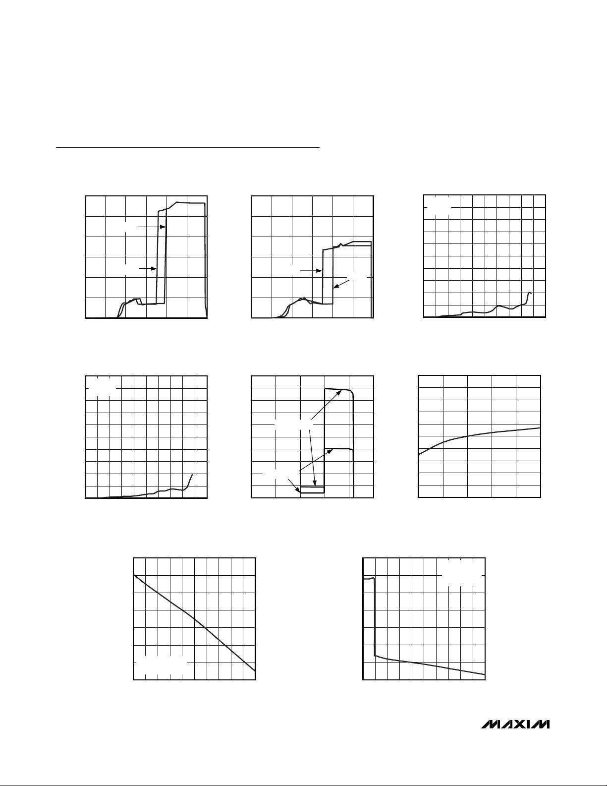
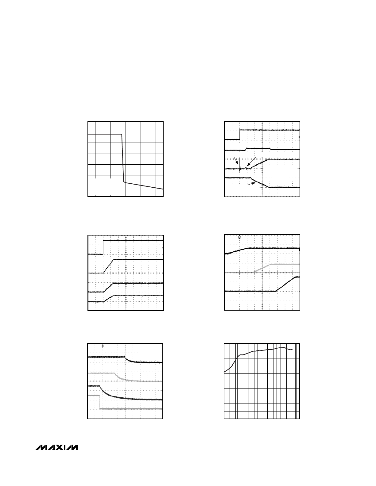
POWER-UP SEQUENCING
(MAX8819A/MAX8819B)
V
EN123
V
V1
MAX8819A toc11
MAX8819A toc09
2V/div
0V
2V/div
0V
V
DC
V
SYS
I
DC
I
BAT
V
V3
V
V2
AC-TO-DC ADAPTER CONNECT
CHARGING
4.3V
C
SYS
400μs/div
3.84V
C
DC
BATTERY CHARGER
SOFT-START
POWER-UP SEQUENCING
(MAX8819C/MAX8819D)
MAX8819A toc10
4V
CHARGING
NEGATIVE BATTERY
CURRENT FLOWS
INTO THE
BATTERY
1A
-1A
MAX8819A toc12
5V/div
2V/div
1A/div
1A/div
2V/div
0V
2V/div
0V
V
V2
V
V3
2ms/div
POWER-DOWN SEQUENCING
(MAX8819C/MAX8819D)
V
V3
V
V2
V
V1
V
RST1
100μs/div
MAX8819A toc13
IV3 = 200mA
= 180mA
I
V2
= 220mA
I
V1
2V/div
0V
2V/div
0V
2V/div
0V
2V/div
0V
2V/div
0V
2V/div
0V
V
V1
1ms/div
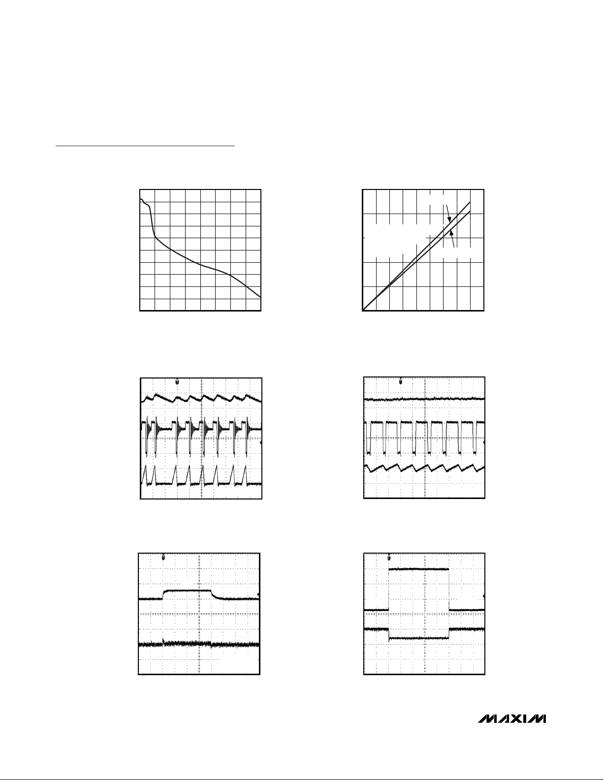
REG1 EFFICIENCY
vs. LOAD CURRENT (V
100
90
80
70
60
50
40
30
REG1 EFFICIENCY (%)
20
10
0
0.1 1 10 100 1000
LOAD CURRENT (mA)
REG1
= 3.01V)
2V/div
0V
MAX8819A toc14
MAX8819A–MAX8819D
PMIC with Integrated Chargers and Smart
Power Selector in a 4mm x 4mm TQFN
10 ______________________________________________________________________________________
Typical Operating Characteristics (continued)
(TA = +25°C, unless otherwise noted.)
REG1 LIGHT-LOAD SWITCHING
WAVEFORMS
MAX8819A toc17
2μs/div
20mV/div
AC-COUPLED
0V
0mA
2V/div
100mA/div
I
LX1
V
LX1
V
OUT1
20mA LOAD
REG1 HEAVY-LOAD SWITCHING
WAVEFORMS
MAX8819A toc18
400ns/div
20mV/div
AC-COUPLED
0V
0mA
2V/div
200mA/div
I
LX1
V
LX1
V
OUT1
200mA LOAD
LINE TRANSIENT
MAX8819A toc19
100μs/div
4V 4V
5V
2V/div
50mV/div
AC-COUPLED
V
OUT1
V
SYS
V
OUT1
= 3V
I
OUT1
= 30mA
REG1 LOAD TRANSIENT (V
OUT
= 3V)
MAX8819A toc20
200μs/div
30mA
300mA
30mA
100mA/div
100mV/div
3V DC OFFSET
V
OUT1
I
OUT1
REG1 LOAD REGULATION
3.09
3.08
3.07
3.06
3.05
3.04
3.03
3.02
REG1 OUTPUT VOLTAGE (V)
3.01
3.00
2.99
0 50 100 150 200 250 300 350 400
REG1 LOAD CURRENT (mA)
MAX8819A toc15
250
200
150
100
DROPOUT VOLTAGE (mV)
50
0
REG1 DROPOUT VOLTAGE
vs. LOAD CURRENT
V
= 3V
OUT1
SYS IS 100mV BELOW THE
REG1 NOMINAL
REGULATION
VOLTAGE
0 50 100 150 200 250 300 350 400 450
OUTPUT CURRENT (mA)
V
OUT1
MAX8819A toc16
= 3.3V
MAX8819A–MAX8819D
PMIC with Integrated Chargers and Smart
Power Selector in a 4mm x 4mm TQFN
______________________________________________________________________________________ 11
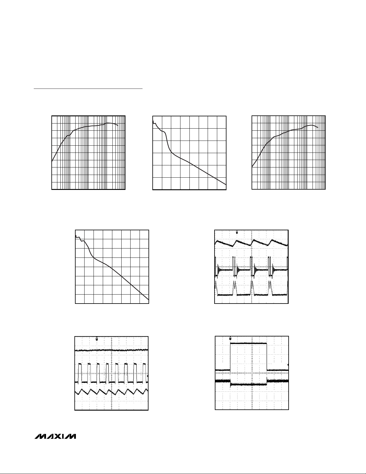
Typical Operating Characteristics (continued)
(TA = +25°C, unless otherwise noted.)
REG2 EFFICIENCY
vs. LOAD CURRENT (V
REG2
= 1.82V)
LOAD CURRENT (mA)
REG2 EFFICIENCY (%)
MAX8819A toc21
0
10
20
30
40
50
60
70
80
90
100
0.1 1 10 100 1000
REG2 LOAD REGULATION
REG2 LOAD CURRENT (mA)
REG2 OUTPUT VOLTAGE (V)
MAX8819A toc22
0 50 100 150 200 250 300 350 400
1.80
1.81
1.82
1.83
1.84
1.85
1.86
REG3 EFFICIENCY
vs. LOAD CURRENT (V
REG3
= 1.21V)
LOAD CURRENT (mA)
REG3 EFFICIENCY (%)
MAX8819A toc23
0
10
20
30
40
50
60
70
80
90
100
0.1 1 10 100 1000
REG3 LOAD REGULATION
REG3 LOAD CURRENT (mA)
REG3 OUTPUT VOLTAGE (V)
MAX8819A toc24
0 50 100 150 200 250 300 350 400
1.185
1.190
1.195
1.200
1.205
1.210
1.215
1.220
1.225
REG3 HEAVY-LOAD SWITCHING
WAVEFORMS
MAX8819A toc26
400ns/div
20mV/div
AC-COUPLED
2V/div
0V
0mA
200mA/div
V
OUT3
V
LX3
I
LX3
200mA LOAD
REG3 LIGHT-LOAD SWITCHING
WAVEFORMS
MAX8819A toc25
2μs/div
20mV/div
AC-COUPLED
2V/div
0V
0mA
100mA/div
V
OUT3
V
LX3
I
LX3
20mA LOAD
REG3 LOAD TRANSIENT
MAX8819A toc27
200μs/div
100mA/div
100mV/div
1.2V DC OFFSET
30mA 30mA
320mA
I
OUT3
V
OUT3

MAX8819A–MAX8819D
PMIC with Integrated Chargers and Smart
Power Selector in a 4mm x 4mm TQFN
12 ______________________________________________________________________________________
Typical Operating Characteristics (continued)
(TA = +25°C, unless otherwise noted.)
LED EFFICIENCY vs. SYS VOLTAGE
SYS VOLTAGE (V)
LED EFFICIENCY (%)
MAX8819A toc28
2.5 3.0 3.5 4.0 4.5 5.0 5.5
50
55
60
65
70
75
80
85
90
95
100
6 LEDS
4 LEDS
I
LED
= 25mA
INDUCTOR: TOKO 1096AS-100M
DIODE: NXP PMEG3005EB
LED EFFICIENCY
vs. LED CURRENT (6 LEDS)
LED CURRENT (mA)
LED EFFICIENCY (%)
MAX8819A toc29
0 5 10 15 20 25
0
10
20
30
40
50
60
70
80
90
100
V
SYS
= 3.6V
LED EFFICIENCY
vs. LED CURRENT (4 LEDS)
LED CURRENT (mA)
LED EFFICIENCY (%)
MAX8819A toc30
0 5 10 15 20 25
0
10
20
30
40
50
60
70
80
90
100
V
SYS
= 3.6V
LED AND BOOST EFFICIENCY
vs. SYS VOLTAGE
SYS VOLTAGE (V)
EFFICIENCY (%)
MAX8819A toc31
2.5 3.0 3.5 4.0 4.5 5.0 5.5
50
55
60
65
70
75
80
85
90
95
100
I
LED
= 25mA
6 LEDS
INDUCTOR: TOKO 1096AS-100M
DIODE: NXP PMEG3005EB
BOOST
LED
REG4 INPUT CURRENT
vs. SYS VOLTAGE
SYS VOLTAGE (V)
REG4 INPUT CURRENT (mA)
MAX8819A toc32
2.5 3.0 3.5 4.0 4.5 5.0 5.5
0
50
100
150
200
250
300
6 LEDS, 100% BRIGHTNESS
REG4 STARTUP AND SHUTDOWN
RESPONSE
MAX8819A toc33
2ms/div
2V/div
10V/div
0V
0mA
10mA/div
V
EN
V
OVP4
I
LED
FB4 VOLTAGE vs. LED CURRENT
LED CURRENT (mA)
FB4 VOLTAGE (mV)
MAX8819A toc34
0 5 10 15 20 25
0
50
100
150
200
250
300
350
400
450
500

MAX8819A–MAX8819D
PMIC with Integrated Chargers and Smart
Power Selector in a 4mm x 4mm TQFN
______________________________________________________________________________________
13
Typical Operating Characteristics (continued)
(TA = +25°C, unless otherwise noted.)
MAXIMUM LED CURRENT
vs. TEMPERATURE
TEMPERATURE (°C)
LED CURRENT (mA)
MAX8819A toc35
-40 -15 10 35 60 85
24.5
24.6
24.7
24.8
24.9
25.0
25.1
25.2
25.3
25.4
25.5
MINIMUM LED CURRENT
vs. TEMPERATURE
TEMPERATURE (°C)
LED CURRENT (mA)
MAX8819A toc36
-40 -15 10 35 60 85
0.730
0.735
0.740
0.745
0.750
Pin Description
PIN NAME FUNCTION
1 COMP4 External Compensation Capacitor for REG4
2 FB4 REG4 Feedback Input
3 OVP4 Overvoltage Protection Node for REG4
4 PG4 REG4 Power Ground
5 LX4 Inductor Switching Node for REG4
6 GND Analog Ground
7 EN4 REG4 Enable Input and Dimming Control Digital Input
8 RST1
9 BAT
10 SYS
11 DC
12 CEN Battery Charger Enable Input
13 FB1
Active-Low, Open-Drain Reset Output. RST1 pulls low to indicate that FB1 is below its regulation
threshold. RST1 goes high 200ms after FB1 reaches its regulation threshold. RST1 is high-impedance
when EN123 is low, and DC is unconnected.
Positive Battery Terminal Connection. Connect BAT to the positive terminal of a single-cell Li+/Li-Poly
battery. Bypass BAT to GND with a 4.7μF ceramic capacitor.
System Supply Output. Bypass SYS to GND with a 10μF ceramic capacitor. When a valid voltage is
present at DC and DLIM[1:2] ≠ 11, V
(MAX8819B/MAX8819D). When the system load (I
75mV (V
BSREG
) below V
, allowing both the external power source and the battery to service SYS.
BAT
SYS is connected to BAT through an internal 70mΩ system load switch when a valid source is not
present at DC.
DC Power Input. DC is capable of delivering 1A to SYS. DC supports both AC adapters and USB
inputs. As shown in Table 1, the DC current limit is controlled by DLIM1 and DLIM2.
Feedback Input for REG1. Connect FB1 to the center of a resistor voltage-divider from the REG1
output capacitors to GND to set the output voltage from 1V to V
is limited to 4.35V (MAX8819A/MAX8819C) or 5.3V
SYS
) exceeds the input current limit, V
SYS
.
SYS
SYS
drops

MAX8819A–MAX8819D
PMIC with Integrated Chargers and Smart
Power Selector in a 4mm x 4mm TQFN
14 ______________________________________________________________________________________
Pin Description (continued)
PIN NAME FUNCTION
14 CISET
15 CHG
16 PG1 REG1 Power Ground
17 LX1
18 PV13
19 LX3
20 PG3 REG3 Power Ground
21 DLIM1
22 FB2
23 FB3
24 EN123
25 PV2 Power Input for REG2. Connect PV2 to SYS. Bypass PV2 to PG2 with a 4.7μF ceramic capacitor.
26 LX2
27 PG2 REG2 Power Ground
28 DLIM2
— EP Exposed Pad
Charge Rate Select Input. Connect a resistor from CISET to GND (R
current limit, prequalification-charge current limit, and top-off threshold.
Active-Low, Open-Drain Charge Status Output. CHG pulls low to indicate that the battery is charging.
See Figure 3 for more information.
Inductor Switching Node for REG1. When enabled, LX1 switches between PV13 and PG1 to regulate
the FB1 voltage to 1.0V. When disabled, LX1 is pulled to PG1 by 1kΩ in shutdown.
Power Input for the REG1 and REG3 Converters. Connect PV13 to SYS. Bypass PV13 to PG1 with a
4.7μF ceramic capacitor.
Inductor Switching Node for REG3. When enabled, LX3 switches between PV13 and PG3 to regulate
the FB3 voltage to 1.0V. When disabled, LX3 is pulled to PG3 by a 1kΩ internal resistor.
Input Current-Limit Selection Digital Input 1. Drive high or low according to Table 1 to set the DC input
current limit.
Feedback Input for REG2. Connect FB2 to the center of a resistor voltage-divider from the REG2
output capacitors to GND to set the output voltage from 1V to V
Feedback Input for REG3. Connect FB3 to the center of a resistor voltage-divider from the REG3
output capacitors to GND to set the output voltage from 1V to V
RE G1, RE G2, and RE G3 E nab l e Inp ut. D r i ve E N 123 hi g h to enab l e RE G1, RE G 2, and RE G3. D r i ve E N 123
l ow to d i sab l e RE G 1, RE G2, and RE G 3. The enab l e/d i sab l e seq uenci ng i s show n i n Fi g ur es 6 and 7.
Inductor Switching Node for REG2. When enabled, LX2 switches between PV2 and PG2 to regulate
the FB2 voltage to 1.0V. When disabled, LX2 is pulled to PG2 by a 1kΩ internal resistor.
Input Current-Limit Selection Digital Input 2. Drive high or low according to Table 1 to set the DC input
current limit.
SYS
SYS
) to set the fast-charge
CISET
.
.

MAX8819A–MAX8819D
PMIC with Integrated Chargers and Smart
Power Selector in a 4mm x 4mm TQFN
______________________________________________________________________________________ 15
Detailed Description
The MAX8819_ is a complete power solution that
includes a battery charger, step-down converters, and
WLED power. As shown in Figure 1, the IC integrates a
DC power input, Li+/Li-Poly battery charger, three stepdown converters, and one step-up converter for powering
white LEDs. All three step-down converters feature
adjustable output voltages set with external resistors.
The MAX8819_ has one external power input that connects to either an AC-to-DC adapter or USB port. Logic
inputs DLIM1 and DLIM2 select the desired input current limit.
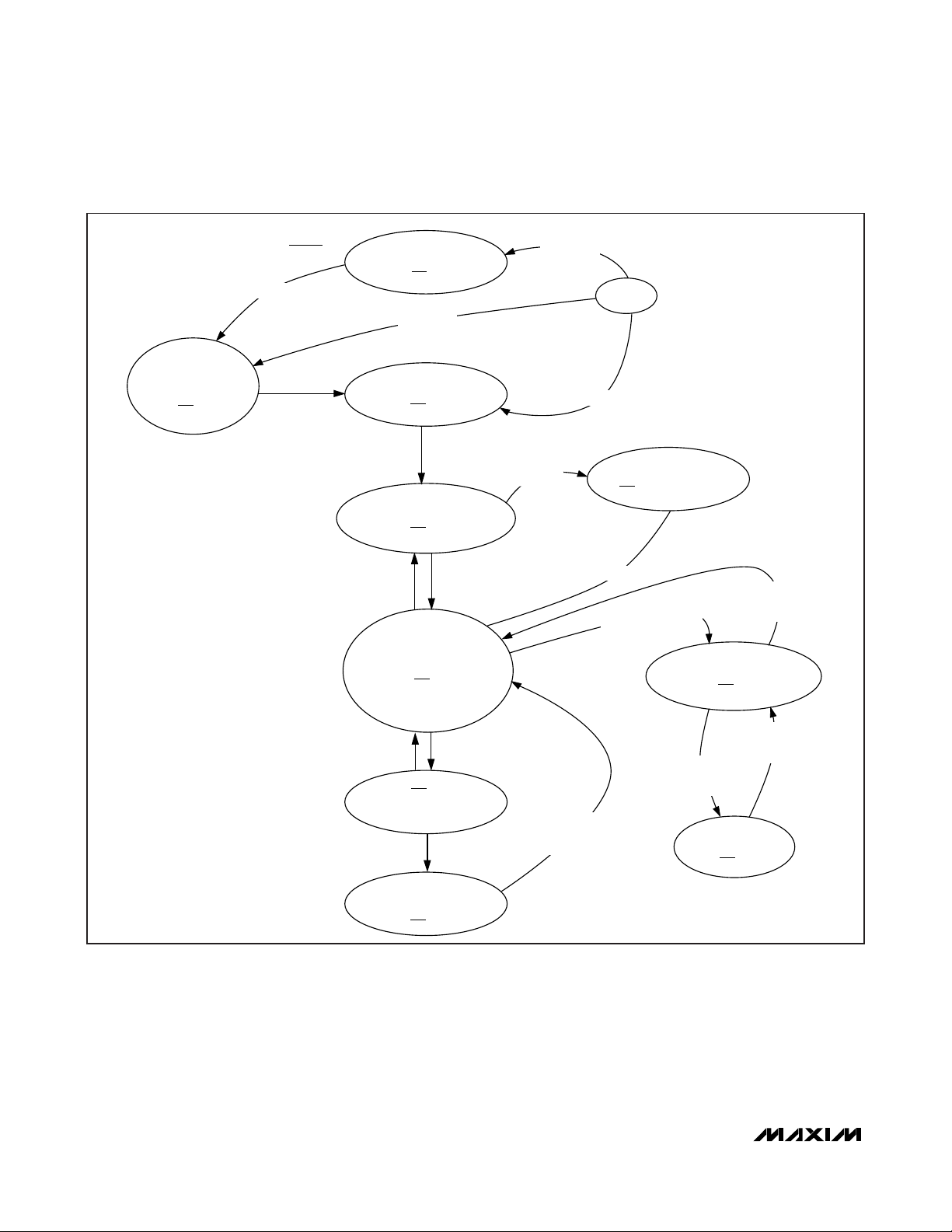
Figure 1. Functional Diagram/Typical Applications Circuit
AC-TO-DC
ADAPTER
DLIM1
DLIM2
00
0
195
1
ON
L4
0.1μF
C2
0.1μF
50V
X7R
C3
PG4
UP TO 6
WLED
10μH
PG4
(25mA)
SYS
OUT4
BATTERY
DESIRED
CAPACITY
(mAh)
300
400
600
800
900
Li+/LiPo
BATTERY
OUT1
R6
470kΩ
C8*
10μF
PG1
OUT1
R10
470kΩ
CHARGE
RATE (C)
0.7
0.7
0.7
0.7
0.7
ON
CHG
3.0V
400mA
OUT1
RST1
1.8V
200mA
C10*
10μF
PG2
300mA
OUT3
C11*
10μF
PG3
DC
C1
4.7μF
SMART
POWER
REG4
STEP-UP
DC-DC
PULSE
DIMMING
SELECTOR
GLITCH FILTER
MAX8819A
MAX8819B
MAX8819C
MAX8819D
AGND
BIAS
DC I
(mA)
LIM
DLIM1
1000
1
475
D1
D2
D3
D4
D5
D6
OFF
0.022μF
DLIM2
EN123
LX4
OVP4
PG4
PG4
COMP4
C4
FB4
EN4
OFF
0
SUSPEND
1
D7
R1
20
ON
EP
Li+/Li-Poly
BATTERY
CHARGER AND
SYSTEM LOAD
SWITCH
PV13
EN
PWM
EN
PWM
PV13
EN
PWM
REG1
STEP-DOWN
DC-DC
REG1/RESET
87% FALLING
50us BLANKING
92% RISING
80ms DELAY
REG2
STEP-DOWN
DC-DC
REG3
STEP-DOWN
DC-DC
SYS
BAT
CEN
CISET
CHG
PV13
LX1
FB1
PG1
RST1
PV2
LX2
FB2
PG2
LX3
FB3
PG3
SYS
C5
10μF
L1
R8
200kΩ
R9
100kΩ
4.7μH
80.6kΩ
4.7
20.0kΩ
100kΩ
L2
R12
R13
100kΩ
L3
R14
R15
+
SYS
SYS
μH
C6
4.7μF
R2
C7
4.7μF
PG1
4.7μH
PG1
C9
4.7μF
PG2
PG2
PG3
R7 (kΩ)
OUT2
1.2V
CHARGE
CURRENT
14.3 210
10.7
7.15
5.36
4.75
OFF
FAST-
(mA)
280
420
560
632
*22μF FOR MAX8819C/MAX8819D IS RECOMMENDED.

MAX8819A–MAX8819D
PMIC with Integrated Chargers and Smart
Power Selector in a 4mm x 4mm TQFN
16 ______________________________________________________________________________________
In addition to charging the battery, the IC supplies
power to the system through the SYS output. The
charging current is provided from SYS so that the set
input current limit controls the total SYS current, this is
the sum of the system load current and the batterycharging current.
In some instances, there may not be enough DC input
current to supply peak system loads. The Smart Power
Selector circuitry offers flexible power distribution from
an AC-to-DC adapter or USB source to the battery and
system load. The battery is charged with any available
power not used by the system load. If a system load
peak exceeds the input current limit, supplemental current is taken from the battery. Thermal limiting prevents
overheating by reducing power drawn from the input
source. In the past, it might have been necessary to
reduce system functionality to limit current drain when a
USB source is connected. However, with the
MAX8819_, this is no longer the case. When the DC or
USB source hits its limit, the battery supplies supplemental current to maintain the load.
The IC features overvoltage protection. Part of this protection is a 4.35V (MAX8819A/MAX8819C) or 5.3V
(MAX8819B/MAX8819D) voltage limiter at SYS. If DC
exceeds the overvoltage threshold of 5.88V (V
OVLO_DC
),
the input limiter disconnects SYS from DC, but batterypowered operation of all regulators is still allowed.
Input Limiter
The Smart Power Selector seamlessly distributes power
between the current-limited external input (DC), the battery (BAT), and the system load (SYS). The basic functions performed are:
With both an external power supply (DC) and battery
(BAT) connected:
• When the system load requirements are less than
the input current limit, the battery is charged with
residual power from the input.
• When the system load requirements exceed the
input current limit, the battery supplies supplemental current to the load through the internal system load switch.
• When the battery is connected and there is no
external power input, the system (SYS) is powered
from the battery.
• When an external power input is connected and
there is no battery, the system (SYS) is powered
from the external power input.
A thermal-limiting circuit reduces the battery charge
rate and external power source current to prevent the
MAX8819_ from overheating.
System Load Switch
An internal 70mΩ MOSFET connects SYS to BAT when
no voltage source is available at DC. When an external
source is detected at DC, this switch opens and SYS is
powered from the valid input source through the Smart
Power Selector.
When the system load requirements exceed the input
current limit, the battery supplies supplemental current
to the load through the internal system load switch. If
the system load continuously exceeds the input current
limit, the battery does not charge, even though external
power is connected. This is not expected to occur in
most cases because high loads usually occur only in
short peaks. During these peaks, battery energy is
used, but at all other times the battery charges.
DC Power Input (DC, DLIM1, DLIM2)
DC is a current-limited power input that supplies the
system (SYS) up to 1A. The DC to SYS switch is a linear
regulator designed to operate in dropout. This linear
regulator prevents the SYS voltage from exceeding
5.3V for the MAX8819B/MAX8819D or 4.35V for the
MAX8819A/MAX8819C. As shown in Table 1, DC supports four different current limits that are set with the
DLIM1 and DLIM2 digital inputs. These current limits
are ideally suited for use with AC-to-DC wall adapters
and USB power. The operating voltage range for DC is
4.1V to 5.5V, but it can tolerate up to 6V without damage. When the DC input voltage is below the undervoltage threshold (4V), it is considered invalid. When the
DC voltage is below the battery voltage it is considered
invalid. The DC power input is disconnected when the
DC voltage is invalid. Bypass DC to ground with at least
a 4.7μF capacitor.
Four current settings are provided based upon the settings of DLIM1 and DLIM2, see Table 1. DLIM1 and
DLIM2 are deglitched. This deglitching prevents the
problem of major carry transitions momentarily entering
the suspend state.
Table 1. DC Current-Limit Settings
DLIM1 DLIM2 DC I
0 0 1000
0 1 475
10 95
1 1 Suspend
LIM
(mA)
MAX8819A–MAX8819D
PMIC with Integrated Chargers and Smart
Power Selector in a 4mm x 4mm TQFN
______________________________________________________________________________________ 17
Battery Charger
Figure 2 shows the typical Li+/Li-Poly charge profile for
the MAX8819_, and Figure 3 shows the battery charger
state diagram.
With a valid DC input that is not suspended, the battery
charger initiates a charge cycle once CEN is driven
high. It first detects the battery voltage. If the battery
voltage is less than the prequalification threshold
(3.0V), the charger enters prequalification mode and
charges the battery at 10% of the maximum fast-charge
current while deeply discharged. Once the battery voltage rises to 3.0V, the charger transitions to fast-charge
mode and applies the maximum charge current. As
charging continues, the battery voltage rises until it
Figure 2. Li+/Li-Poly Charge Profile
BATTERY VOLTAGEBATTERY CHARGE CURRENTCHG
V
BATREG
V
BATPRQ
I
CHGMAX
PREQUALIFICATION
I
PQ
FAST-CHARGE
(CONSTANT CURRENT)
FAST-CHARGE
(CONSTANT VOLTAGE)
TOP-OFF
DONE
I
TO
0
HIGH
IMPEDANCE
LOW
MAX8819A–MAX8819D
PMIC with Integrated Chargers and Smart
Power Selector in a 4mm x 4mm TQFN
18 ______________________________________________________________________________________
approaches the battery regulation voltage (4.2V typ)
where charge current starts tapering down. When
charge current decreases to 10% of the maximum fastcharge current, the charger enters a 33min top-off state
and then charging stops. If the battery voltage subsequently drops 100mV below the battery regulation voltage, charging restarts and the timers reset.
The battery charge rate is set by several factors:
• Battery voltage
• DC input current limit
• The charge-setting resistor, R
CISET
• The system load (I
SYS
)
Figure 3. Li+/Li-Poly Charger State Diagram
I
= 2000 x
CHGMAX
DC = VALID
INPUT SUSPENDED
DLIM[1:2] = 11
I
= 0mA
CHG
CHG = 1
1.5V
R
CISET
DLIM[1:2] ≠ 11
NO INPUT POWER
CHARGER DISABLED
PREQUALIFICATION
I
CHG
V
< 2.82V
BAT
IC SETS TIMER = 0
I
CHG
CHG = 1
DLIM[1:2] = 11
I
CHG
CHG = 1
≤ I
CHGMAX
CHG = 0
FAST-CHARGE
I
≤ I
CHG
CHG = 0
= 0mA
= 0mA
CEN = 1
IC SETS TIMER = 0
/10
V
> 3V,
BAT
IC SETS TIMER = 0
CHGMAX
t > t
PREQUAL
DC = INVALID
CEN = 0
ANY STATE
TIMER FAULT
I
= 0mA
CHG
CHG = 2Hz SQUAREWAVE
t > t
FSTCHG
I
< I
CHGMAX
< V
BAT
(I
x 50%
BATREG
CHGMAX
CHG
AND V
IC EXTENDS TIMER BY 2x
TIMER EXTEND
x 20%) < I
CHG = 0
I
< I
CHG
CHGMAX
OR V
BAT
IC RESUMES TIMER
< (I
CHG
CHGMAX
= V
x 50%)
x 53%
BATREG
< I
I
CHG
x 20%
CHGMAX
IC SETS TIMER = 0
t
TOP-OFF
(V
BATREG
TOP-OFF
CHG = 1
V
= V
BAT
I
≤ I
CHG
CHGMAX
>
DONE
-100mV) ≤ V
I
= 0mA
CHG
CHG = 1
< I
I
CHG
CHGMAX
IC SETS TIMER = 0
BATREG
/10
33min
≤ V
BAT
BATREG
x 10% AND V
BAT
V
< (V
BAT
BATREG
100mV)
IC SETS TIMER = 0
I
< I
CHG
AND V
IC SUSPENDS
x 20%
CHGMAX
BAT<VBATREG
TIMER
TIMER SUSPEND
I
< (I
CHG
CHGMAX
CHG = 0
I
< I
x 23%
CHG
SET
OR V
= V
BAT
IC RESUMES TIMER
BATREG
x 20%)

MAX8819A–MAX8819D
PMIC with Integrated Chargers and Smart
Power Selector in a 4mm x 4mm TQFN
______________________________________________________________________________________ 19
• The die temperature
• The battery charger is enabled by the processor driving the CEN input high. A valid input must be available at DC. The battery charger is disabled without
a valid input at DC or by driving CEN low.
• The system current has priority over the battery
charger; the battery charger automatically reduces
its charge current to maintain the input current limit
while still providing the system current (I
SYS
).
• The input current limit is tapered down from full current to zero current when the die temperature transitions from +100°C to +120°C. Since I
SYS
has priority
over the battery charge current, the battery charge
current tapers down before I
SYS
. The overall result is
self-regulation of die temperature (see the
Thermal
Limiting and Overload Protection
section for more
information).
• The battery charger stops charging in done mode
as shown in Figures 2 and 3.
Charge Status Output (CHG)
CHG is an open-drain, active-low output that indicates
charger status. As shown in Figures 2 and 3, CHG is
low when the charger is in its prequalification or fastcharge states. When a timer count is exceeded in
either state, CHG indicates the fault by blinking at a
2Hz rate and remains in that state until the charger is
reset by CEN going low, removal of DC or setting
DLIM[1:2] = 11.
When the MAX8819_ is used with a microprocessor
(μP), connect a pullup resistor between CHG and the
system logic voltage to indicate charge status to the
μP. Alternatively, CHG sinks up to 20mA for an LED
charge indicator.
If the charge status output feature is not required, connect CHG to ground or leave unconnected.
Charge Timer
As shown in Figure 3, a fault timer prevents the battery
from charging indefinitely. In prequalification mode, the
charge time is internally fixed to 33min.
t
PREQUAL
= 33min
In fast-charge mode, the charge timer is internally fixed
to 660min.
t
FSTCHG
= 660min
When the charger exits fast-charge mode, a fixed
33min top-off mode is entered:
t
TOP-OFF
= 33min
While in the constant-current fast-charge mode (Figure
2), if the MAX8819_ reduces the battery charge current
due to its internal die temperature or large system
loads, it slows down the charge timer. This feature eliminates nuisance charge timer faults. When the battery
charge current is between 100% and 50% of its programmed fast-charge level, the fast-charge timer runs
at full speed. When the battery charge current is
between 50% and 20% programmed fast-charge level,
the fast-charge timer is slowed by 2x. Similarly, when
the battery charge current is below 20% of the programmed fast-charge level, the fast-charge timer is
Figure 4. Calculated Charge Currents vs. R
CISET
Table 2. Calculated Charge Currents vs.
R
CISET
FAST-CHARGE, PREQUALIFICATION, AND TOP-OFF
CURRENT vs. CHARGE-SETTING RESISTOR
10,000
I
1000
100
CURRENT (mA)
10
1
0 5 10 15 20
CHGMAX
I
PREQUAL, ITOP-OFF
R
CISET
(kΩ)
I
R
(kΩ)
CISET
3.01 1000 100 100
4.02 746 75 75
4.99 601 60 60
6.04 497 50 50
6.98 430 43 43
8.06 372 37 37
9.09 330 33 33
10 300 30 30
11 273 27 27
12.1 248 25 25
13 231 23 23
14 214 21 21
15 200 20 20
CHGMAX
(mA)
I
(mA) I
PQ
TO
(mA)

MAX8819A–MAX8819D
PMIC with Integrated Chargers and Smart
Power Selector in a 4mm x 4mm TQFN
20 ______________________________________________________________________________________
paused. The fast-charge timer is not slowed or paused
when the charger is in the constant voltage portion of
its fast-charge mode (Figure 2) where the charge current reduces normally.
Charge Current (CISET)
As shown in Table 2 and Figure 4, a resistor from CISET
to ground (R
CISET
) sets the maximum fast-charge cur-
rent (I
CHGMAX
), the charge current in prequalification
mode (I
PREQUAL
), and the top-off threshold (I
TOP-OFF
).
The MAX8819_ supports values of I
CHGMAX
from 200mA
to 1000mA. Select the R
CISET
as follows:
Determine I
CHGMAX
by considering the characteristics
of the battery. It is not necessary to limit the charge current based on the capabilities of the expected AC-toDC adapter or USB/DC input current limit, the system
load, or thermal limitations of the PCB. The IC automatically lowers the charging current as necessary to
accommodate for these factors.
For the selected value of R
CISET
, calculate I
CHGMAX
,
I
PREQUAL
, and I
TOP-OFF
as follows:
Step-Down Converters
(REG1, REG2, REG3)
REG1, REG2, and REG3 are high-efficiency, 2MHz current-mode step-down converters with adjustable outputs.
REG1 is designed to deliver 400mA for the MAX8819A/
MAX8819B and 550mA for the MAX8819C/MAX8819D.
REG2 and REG3 are designed to deliver 300mA for the
MAX8819A/MAX8819B and 500mA for the MAX8819C/
MAX8819D.
The step-down regulator power inputs (PV_) must be
connected to SYS. The step-down regulators operate
with V
SYS
from 2.6V to 5.5V. Undervoltage lockout
ensures that the step-down regulators do not operate
with SYS below 2.55V (max).
See the
Step-Down Converter Enable/Disable (EN123)
and Sequencing
section for how to enable and disable
the step-down converters. When enabled, the
MAX8819_ gradually ramps each output up during a
2.6ms soft-start time. When enabled, the MAX8819C/
MAX8819D sequentially ramps up each output. Softstart eliminates input current surges when regulators
are enabled.
See the
Step-Down Control Scheme
section for informa-
tion about the step-down converters control scheme.
The IC uses external resistor-dividers to set the stepdown output voltages between 1V and V
SYS
. Use at
least 10μA of bias current in these dividers to ensure no
change in the stability of the closed-loop system. To set
the output voltage, select a value for the resistor connected between FB_ and GND (R
FBL
). The recommended value is 100kΩ. Next, calculate the value of the
resistor connected from FB_ to the output (R
FBH
):
REG1, REG2, and REG3 are optimized for high, medium, and low output voltages, respectively. The highest
overall efficiency occurs with V1 set to the highest output voltage and V3 set to the lowest output voltage.
REG2 can be disabled by connecting PV2 to GND.
Step-Down Control Scheme
At light load, the step-down converter switches only as
needed to supply the load. This improves light-load efficiency. At higher load currents (~80mA), the step-down
converter transitions to fixed 2MHz switching.
Step-Down Dropout and Minimum Duty Cycle
All of the step-down regulators are capable of operating in 100% duty-cycle dropout, however, REG1 has
been optimized for this mode of operation. During
100% duty-cycle operation, the high-side p-channel
MOSFET turns on constantly, connecting the input to
the output through the inductor. The dropout voltage
(VDO) is calculated as follows:
where:
R
P
= p-channel power switch R
DS(ON)
R
LSR
= external inductor ESR
The minimum duty cycle for all step-down regulators is
12.5% (typ), allowing a regulation voltage as low as 1V
over the full SYS operating range. REG3 is optimized
for low duty-cycle operation.
Step-Down Input Capacitor
The input capacitor in a step-down converter reduces
current peaks drawn from the power source and
reduces switching noise in the controller. The impedance of the input capacitor at the switching frequency
must be less than that of the source impedance of the
II
PREQ UAL TOP OF F
2000
15.
I
CHGMAX
R
R
CISET
I
CHGMAX
=×2000
=×
==
−
V
V
1510.
CISET
%% × I
CHGMAX
RR
=× −
FBH FBL
V
⎛
OUT
⎜
⎝
101.
⎞
⎟
⎠
V
VI RR
=+
DO LOAD P L
()

MAX8819A–MAX8819D
PMIC with Integrated Chargers and Smart
Power Selector in a 4mm x 4mm TQFN
______________________________________________________________________________________ 21
supply so that high-frequency switching currents do not
pass through the input source.
The step-down regulator power inputs are critical discontinuous current paths that require careful bypassing. In the PCB layout, place the step-down converter
input bypass capacitors as close as possible to each
pair of switching converter power input pins (PV_ to
PG_) to minimize parasitic inductance. If making connections to these capacitors through vias, be sure to
use multiple vias to ensure that the layout does not
insert excess inductance or resistance between the
bypass capacitor and the power pins.
The input capacitor must meet the input ripple current
requirement imposed by the step-down converter.
Ceramic capacitors are preferred due to their low ESR
and resilience to power-up surge currents. Choose the
input capacitor so that its temperature rise due to input
ripple-current does not exceed approximately +10°C.
For a step-down DC-DC converter, the maximum input
ripple current is half of the output current. This maximum input ripple current occurs when the step-down
converter operates at 50% duty factor (VIN= 2 x V
OUT
).
Bypass each step-down converter input with a 4.7μF
ceramic capacitor from PV_ to PG_. Use capacitors that
maintain their capacitance over temperature and DC
bias. Ceramic capacitors with an X7R or X5R temperature characteristic generally perform well. The capacitor
voltage rating should be 6.3V or greater.
Step-Down Output Capacitors
The output capacitance keeps output ripple small and
ensures control-loop stability. The output capacitor
must have low impedance at the switching frequency.
Ceramic, polymer, and tantalum capacitors are suitable
with ceramic exhibiting the lowest ESR and lowest highfrequency impedance. The MAX8819A/MAX8819B
require at least 10μF of output capacitance. The
MAX8819C/MAX8819D require ar least 22μF of output
capacitance.
As the case sizes of ceramic surface-mount capacitors
decreases, their capacitance vs. DC bias voltage characteristic becomes poor. Due to this characteristic, it is
possible for 0805 capacitors to perform well while 0603
capacitors of the same value may not. The MAX8819A/
MAX8819B require a nominal output capacitance of
10μF, however, after their DC bias voltage derating, the
output capacitance must be at least 7.5μF.
Step-Down Inductor
Choose the step-down converter inductance to be
4.7μH. The minimum recommended saturation current
requirement is 700mA. In PWM mode, the peak inductor currents are equal to the load current plus one half
of the inductor ripple current. See Table 3 for suggested
inductors.
Table 3. Suggested Inductors
MANUFACTURER SERIES
Sumida
Taiyo Yuden
TDK
TOKO DE2812C 4.7 130 880 3.0 x 2.8 x 1.2 = (10.8mm)
FDK
CDRH2D11HP 4.7 190 750 3.0 x 3.0 x 1.2 = (10.8mm)
CDH2D09 4.7 218 700 3.0 x 3.0 x 1.0= (9.0mm)
NR3012 4.7 130 770 3.0 x 3.0 x 1.2 = (10.8mm)
NR3010 4.7 190 750 3.0 x 3.0 x 1.0 = (9.0mm)
VLF3012 4.7 160 740 2.8 x 2.6 x 1.2 = (8.7mm)
VLF3010 4.7 240 700 2.8 x 2.6 x 1.0 = (7.3mm)
MIPF2520 4.7 110 1100 2.5 x 2.0 x 1.0 = (5mm)
MIPF2016 4.7 160 900 2.0 x 1.6 x 1.0 = (3.2mm)
INDUCTANCE
(µH)
ESR
(mΩ)
CURRENT RATING
(mA)
DIMENSIONS
(mm)
3
3
3
3
3
3
3
3
3

MAX8819A–MAX8819D
PMIC with Integrated Chargers and Smart
Power Selector in a 4mm x 4mm TQFN
22 ______________________________________________________________________________________
The peak-to-peak inductor ripple current during PWM
operation is calculated as follows:
where f
S
is the 2MHz switching frequency.
The peak inductor current during PWM operation is calculated as follows:
Step-Down Converter Maximum Output Current
The maximum regulated output current from a step-down
converter is ultimately determined by the p-channel peak
current limit (IPK). The calculation follows:
I
OUT,MAX
= IPK– (I
P-P
/2)
For example, if V
SYS
= 5.3V, V
OUT
= 3V, fS= 2MHz,
L = 4.7μH, and IPK= 0.6A:
I
P-P
= 3V x (5.3V - 3V)/(5.3V x 2MHz x 4.7μH) = 0.138A
then I
OUT_MAX
= 0.6A - (0.138A/2) = 0.531A.
Figure 5a. MAX8819A/MAX8819B Enable/Disable Logic
SYS
2.5V RISING
100mV HYST.
DIE TEMP
+165°C
DC
6.0V RISING
400mV HYST.
4.0V RISING
500mV HYST.
+
SYSOK
-
+
DT165
-
+
DCOVLO
-
DCUVLO
+
EN123
EN4
2MHz
OSC
BIAS
AND
REF
64 CYCLE
DELAY
(32μs)
READY
REGON
READY
DCPOK
REGON
MAX8819A
MAX8819B
SOFT-START
REG1
EN
SOFT-START
REG2
EN
SOFT-START
REG3
EN
SOFT-START
REG4
EN OK
OK
OK
OK
REG1OK
REG2OK
REG3OK
REG4OK
VV V
I
PP
OUT SYS OUT
=
−
VfL
−
()
××
SYS S
I
PP
II
L PEA K LOAD
=+
_
−
2

MAX8819A–MAX8819D
PMIC with Integrated Chargers and Smart
Power Selector in a 4mm x 4mm TQFN
______________________________________________________________________________________ 23
As the load current is increased beyond this point, the
output voltage sags and the converter goes out of regulation because the inductor current cannot increase
above the p-channel peak current limit.
Step-Down Converter Short-Circuit Protection
The step-down converter implements short-circuit protection by monitoring the feedback voltage, V
FB_
. After soft-
start, if V
FB_
drops below 0.23V, the converter reduces its
switching frequency to fS/3. The inductor current still
reaches the p-channel peak current limit, however, at
one-third the frequency. Therefore, the output and input
currents are reduced to approximately one-third of the
maximum value in response to an output short circuit to
ground. When the short is removed, the inductor current
raises the voltage on the output capacitor and the stepdown converter resumes normal operation.
REG1 Reset (RST1)
RST1 is an active-low, open-drain output that pulls low
to indicate that FB1 is below its regulation threshold.
RST1 goes high 200ms after FB1 reaches its regulation
threshold. RST1 is high-impedance when EN123 is
high. See Figures 6 and 7.
A 50μs blanking delay is provided when FB1 is falling,
so that RST1 does not glitch if the REG1 output voltage
is dynamically adjusted by altering the resistors in its
feedback network.
Figure 5b. MAX8819C/MAX8819D Enable Logic
SYS
EN123
EN4
+
SYSOK
2.5V RISING
100mV HYST.
DIE TEMP
+165°C
DC
6.0V RISING
400mV HYST.
4.0V RISING
500mV HYST.
-
READY
+
+
-
-
+
DT165
-
DCOVLO
DCPOK
DCUVLO
2MHz
OSC
BIAS
AND
REF
64 CYCLE
DELAY
(32μs)
READY
REGON
REGON
MAX8819C
MAX8819D
SOFT-START
REG1
EN
SOFT-START
REG2
EN
SOFT-START
REG3
EN
SOFT-START
REG4
EN OK
OK
OK
OK
REG1OK
REG2OK
REG3OK
REG4OK

MAX8819A–MAX8819D
PMIC with Integrated Chargers and Smart
Power Selector in a 4mm x 4mm TQFN
24 ______________________________________________________________________________________
Step-Down Converter Active Discharge
in Shutdown
Each MAX8819_ step-down converter (REG1, REG2,
REG3) has an internal 1kΩ resistor that discharges the
output capacitor when the converter is off. The discharge resistors ensure that the load circuitry powers
down completely. The internal discharge resistors are
connected when a converter is disabled and when the
device is in UVLO with an input voltage greater than
1.0V. With an input voltage less than 1.0V the internal
discharge resistors are not activated.
Step-Down Converter Enable/Disable (EN123)
and Sequencing
Figure 5a shows the MAX8819A/MAX8819B enable and
disable logic. Figure 5b shows MAX8819C/MAX8819D
enable/disable logic. Figure 6 shows an example of
enable and disable waveforms for the MAX8819A/
MAX8819B.
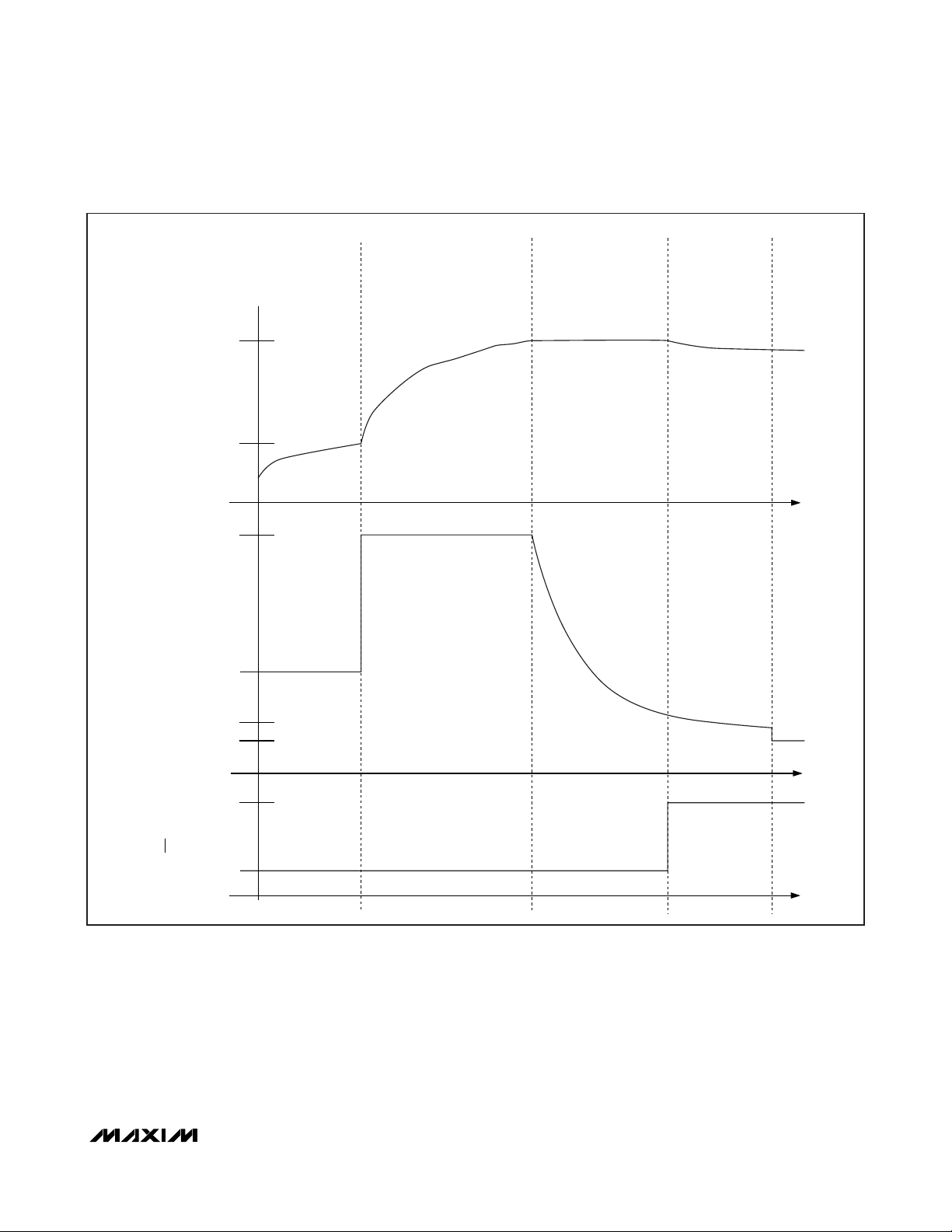
Figure 6 notes:
1) The device is off with no external power applied to
DC. The system voltage (V
SYS
) is equal to the bat-
tery voltage (V
BAT
).
2) An external supply is applied to DC that causes the
step-down converter to power up after the DC-toSYS soft-start time (t
SS-D-S
). When the DC input is
valid and DLIM[1:2] ≠ 11, V
SYS
increases.
3) When V1 reaches the reset trip threshold (V
THRST
),
the reset deassert delay timer starts. When the reset
deassert delay timer expires (t
DRST1
), RST1 goes
high-impedance. If RST1 is connected to the RESET
Figure 6. MAX8819A/MAX8819B Enable/Disable Waveforms Example
NOTES
V
V
V
V
V
V
V
SYS
EN123
OUT1
OUT2
OUT3
RST1
DC
12
V
BAT
t
SS-D-S
34
V
BAT
t
SS1
t
SS2
t
SS3
V
EN4
V
V
OUT4
SYS
- V
D
5
6
< V
< V
SYS
DC
HIGH
IMPEDANCE
t
DRST1
t
SS4
78
V
BAT
V
SYS
- V
D
V
CEN
V
CHG
t
SS_CHG

MAX8819A–MAX8819D
PMIC with Integrated Chargers and Smart
Power Selector in a 4mm x 4mm TQFN
______________________________________________________________________________________ 25
input of the system μP, the processor can begin its
boot-up sequence up at this time.
4) During the μP’s boot-up sequence, it asserts EN123
to keep the step-down converters enabled, even if
DC is removed.
5) After the μP has booted, it asserts EN4 to turn on the
display’s backlight.
6) CEN is asserted by the μP to start a charge cycle.
7) The external supply is removed from DC and V
SYS
falls. The converters remain enabled because the μP
has asserted EN123 and EN4, but the battery charging current drops to zero even though CEN is still
asserted. CHG goes high impedance.
8) System is turned off by deasserting EN123, EN4, and
CEN; RST1 goes low to reset the μP.
Figure 7 notes:
1) The MAX8819C/MAX8819D are off with no external
power applied to DC. The system voltage (V
SYS
) is
equal to the battery voltage (V
BAT
).
2) An external supply is applied to DC that causes the
step-down regulator to power up after the DC-toSYS soft-start time (t
SS-D-S
). When the DC input is
valid and DC is not suspended, V
SYS
rises.
3) EN123 is pulled high to start the OUT3, OUT2, and
OUT1 power-up sequence. When OUT1 reaches the
reset trip threshold (V
THRST
), the reset deassert
delay timer starts. When the reset deassert delay
timer expires (t
DRST1
200ms typ.), RST1 goes high-
impedance. If RST1 is connected to the RESET input
of the system μP, the processor can begin its bootup sequence at this time.
Figure 7. MAX8819C/MAX8819D Enable/Disable Waveforms Example
NOTES
V
V
V
V
V
V
V
V
EN123
OUT3
OUT2
OUT1
RST1
V
OUT4
DC
SYS
EN4
12
V
BAT
t
SS-D-S
34
V
< V
< V
BAT
SYS
DC
2.6ms
2.6ms
2.6ms
V
- V
SYS
D
5
HIGH IMPEDANCE
200ms
t
SS4
6
V
BAT
7
V
- V
SYS
D
V
CEN
V
CHG
t
SS_CHG

MAX8819A–MAX8819D
PMIC with Integrated Chargers and Smart
Power Selector in a 4mm x 4mm TQFN
26 ______________________________________________________________________________________
4) EN4 to turn on the display’s backlight.
5) CEN is asserted by the μP to start a charge cycle.
6) The external supply is removed from DC and V
SYS
falls. The regulators remain enabled because EN123
and EN4 are asserted, but the battery charging current drops to zero even though CEN is still asserted.
CHG goes high-impedance.
7) System is turned off by deasserting EN123, EN4,
and CEN. OUT1, OUT2, and OUT3 power down in
the opposite order of power-up. RST1 goes low to
reset the μP.
Step-Up Converter (REG4)
The step-up converter (REG4) operates by regulating
the voltage at FB4 to 0.5V. REG4 operates from the
system voltage (V
SYS
); this voltage can vary from 2.6V to
4.35V (MAX8819A/MAX8819C) or 5.3V (MAX8819B/
MAX8819D). The 1MHz switching frequency allows for
tiny external components. The step-up converter control
scheme optimizes the efficiency while achieving low EMI
and low input ripple.
REG4 WLED Driver Configuration
Figure 1 shows that REG4 is configured as a white light
emitting diodes (WLED) driver, typically used to drive
up to six devices with an output voltage up to 24V. The
full-scale current is set by resistor R1, according to the
following relationship:
Figure 8. Dimming Control Timing Diagram
Table 4. REG4 Recommended Inductors
Table 5. REG4 Recommended Diodes
t
HI_INIT
> 100μs
t
SOFT-START
SHUTDOWN
0
STEP
EN4
I
LED
1 3332313029285432
FULL
31/32
30/32
29/32
500ns TO 500μs
28/32
27/32
t
t
6/32
HI
> 500ns
5/32
LO
V
FB
I
FS
IV mA
FS
4/32
4
==
<=
3/32
, . min
where V V no ally
1
R
0 5 16 30 9
./ .Ω
FULL
2/32
1/32
FB
4
31/32
05
t
SHDN
2ms (typ)
SHUTDOWN
MANUFACTURER SERIES
TOKO
FDK MIP3226 10 160 900 3.2 x 2.6 x 1 = (8.32mm)
DE2812C 10 290 580 3.0 x 2.8 x 1.2 = (10.8mm)
DB3018C 10 240 630 3.2 x 3.2 x 1.8 = (18.4mm)
INDUCTANCE
(µH)
ESR (mΩ)
CURRENT
RATING (mA)
DIMENSIONS (mm)
CONTINUOUS
MANUFACTURER PART NUMBER
Central Semiconductor
NXP PMEG3005EB 500 500 30 SOD-523
ON Semiconductor MBR0530L 500 430 30 SOD-123
CMDSH05-4 500 470 40 SOD-323
CMHSH5-4 500 510 40 SOD-123
CURRENT
(mA)
FORWARD VOLTAGE
(mV)
BREAKDOWN
VOLTAGE
(V)
PACKAGE
3
3
3

MAX8819A–MAX8819D
PMIC with Integrated Chargers and Smart
Power Selector in a 4mm x 4mm TQFN
______________________________________________________________________________________ 27
EN4 enables REG4, disables REG4, and adjusts the voltage on FB4 in 32 linear steps. If current adjustment is not
required, EN4 acts as a simple enable/disable controller.
Driving EN4 high for at least 100μs powers up REG4 and
sets V
FB4
to 0.5V. Pulling EN4 low for at least 2ms dis-
ables REG4. To adjust V
FB4
, apply pulses as shown in
Figure 8. Dim the WLEDs by pulsing EN4 low (500ns to
500μs pulse width). Each pulse reduces the LED current
by 1/32. Note: When REG4 is disabled, OUT4 is equal to
V
SYS
minus the drop from the catch diode.
In the event that the load (typically WLEDs) opens,
V
OUT4
rises quickly until it reaches the overvoltage protection threshold (typically 25V). When this occurs,
REG4 stops switching and latches off until EN4 is reset
low for at least 2ms.
Step-Up Converter Inductor Selection
The WLED boost converter switches at 1MHz, allowing
the use of a small inductor. A 10μH inductance value is
recommended for most applications. Smaller inductances require less PCB space.
Use inductors with a ferrite core or equivalent.
Powdered iron cores are not recommended for use at
high-switching frequencies. The inductor’s saturation
current rating should preferably exceed the REG4
n-channel current limit of 700mA. Choose an inductor
with a DC resistance less than 300mΩ to maintain high
efficiency. Table 4 lists recommended inductors.
Step-Up Converter Diode Selection
The REG4 diode must be fast enough to support the
switching frequency (1MHz). Schottky diodes, such as
Central Semiconductor’s CMHSH5-4 or ON Semiconductor’s MBR0530L, are recommended. Make sure that
the diode’s peak-current rating matches or exceeds the
700mA REG4 n-channel current limit. The diode’s average current rating should match or exceed the output
current. The diode’s reverse breakdown voltage must
exceed the voltage from the converter’s output to
ground. Schottky diodes are preferred due to their low
forward voltage, however, ultra high-speed silicon rectifiers are also acceptable.
Step-Up Converter Output Capacitor Selection
For most applications, a 0.1μF ceramic output filter
capacitor is suitable. Choose a voltage rating double
the maximum output voltage to minimize the effect of
the voltage coefficient on decreasing the effective
capacitance. To ensure stability over a wide temperature range, ceramic capacitors with an X5R or X7R
dielectric are recommended. Place these capacitors as
close as possible to the IC.
Soft-Start/Inrush Current
The MAX8819_ implements soft-start on many levels to
control inrush current to avoid collapsing supply voltages, and to fully comply with the USB 2.0 specifications. All DC and charging functions implement soft-start.
The DC node only requires 4.7μF of input capacitance.
Furthermore, all regulators implement soft-start to avoid
transient overload of power inputs.
Undervoltage and Overvoltage Conditions
DC UVLO
DC undervoltage lockout (UVLO) prevents an input supply from being used when its voltage is below the operating range. When the voltage from DC to GND (VDC) is
less than the DC UVLO threshold (4.0V, typ), the DC
input is disconnected from SYS, the battery charger is
disabled and CHG is high impedance. BAT is connected
to SYS through the internal system load switch in DC
UVLO mode, allowing the battery to power the SYS
node. REG1–REG4 and the LED current sinks are
allowed to operate from the battery in DC UVLO mode.
DC OVLO
DC overvoltage lockout (OVLO) is a fail-safe mechanism and prevents an input supply from being used
when its voltage exceeds the operating range. The
absolute maximum ratings state that DC withstands
voltages up to 6V. Systems must be designed so that
DC never exceeds 6V (transient and steady-state). If
the voltage from DC to GND (VDC) should exceed the
DC OVLO threshold (5.9V typ) during a fault, the DC
input is disconnected from SYS, the battery charger is
disabled, and CHG is high impedance. BAT is connected to SYS through the internal system load switch in DC
OVLO mode, allowing the battery to power SYS through
the internal system load switch in DC OVLO mode.
REG1–REG4 are allowed to operate from the battery in
DC OVLO mode. Normal operation resumes when V
DC
falls within its normal operating range.
SYS UVLO
SYS undervoltage lockout (UVLO) prevents the regulators from being used when the input voltage is below
the operating range. When the voltage from SYS to
GND (V
SYS
) is less than the SYS UVLO threshold (2.5V,
typ), REG1–REG4, the LED current sinks, and the battery charger are disabled. Additionally, CHG, is high
impedance and RST1 is asserted.
Thermal Limiting and Overload Protection
Smart Power Selector Thermal-Overload Protection
The IC reduces the DC current limit by 5%/°C when the
die temperature exceeds +100°C. The system load
(I
SYS
) has priority over the charger current, so input

MAX8819A–MAX8819D
PMIC with Integrated Chargers and Smart
Power Selector in a 4mm x 4mm TQFN
28 ______________________________________________________________________________________
current is first reduced by lowering charge current. If
the junction temperature still reaches +120°C in spite of
charge current reduction, no input current is drawn
from DC; the battery supplies the entire load and SYS is
regulated 70mV below BAT.
Regulator Thermal-Overload Shutdown
The IC disables all regulator outputs and the battery
charger when the junction temperature rises above
+165°C, allowing the device to cool. When the junction
temperature cools by approximately 15°C the regulators and charger resume the state indicated by the
enable input (EN123, EN4, and CEN) by repeating their
soft-start sequence. Please note that this thermal-overload shutdown is a fail-safe mechanism; proper thermal
design should ensure that the junction temperature of
the MAX8819_ never exceeds the absolute maximum
rating of +150°C.
Applications Information
Dynamic Output Voltage Adjustment for
Step-Down Converters
Dynamic output voltage adjustment can be implemented for the step-down converter by adding a resistor
and a switch from FB_ to GND. See Figure 9.
To calculate the resistor-divider, start with the lower
voltage desired and calculate the resistor-divider using
RTand RBonly. Setting RB= 100kΩ is acceptable. Use
the following equation to calculate RT:
where V
OUTL
is the desired lower output voltage and
VFBis the feedback regulation voltage, 1V (typ).
R
D
is calculated using the higher set voltage and the
following equations assuming the switch resistance is
negligible:
where R
PAR
is the parallel resistance of RBand RD,
V
OUTH
is the higher set voltage, and VFBis the feed-
back regulation voltage, 1V (typ).
For example, if V
OUTL
= 3V, V
OUTH
= 3.3V, RB=
100kΩ, then:
R
T
= 100kΩ x ((3V/1V) - 1) = 200kΩ
R
PAR
= 200kΩ/((3.3V/1V) - 1) = 86.96kΩ
RD= 1/((1/86.96kΩ) - (1/100kΩ)) = 666.7kΩ
Choose RD= 665kΩ as the closest standard 1% value.
CH1 = gate drive to switch
CH2 = V1, 1V offset; 3V to 3.3V to 3V, 10Ω load
CH3 = RST1
The scope plot (Figure 10) shows V1 switching from 3V
to 3.3V to 3V with the resistor values of the example.
When the switch is turned on, V1 slews from 3V to 3.3V
in about 20μs, which is less than the 50μs RST1 de-
glitch filter, and therefore, RST1 does not trip. When the
switch is turned off, V1 soars to about 3.35V due to the
energy in the inductor. Since V1 is above the regulation
voltage, REG1 skips until V1 decays to the regulation
voltage. The decay rate is determined by the output
capacitance and the load. In this example, the output
capacitance is 10μF and the load is 10Ω, so the time
Figure 9. Dynamic Output Voltage Control
Figure 10. Dynamic Voltage Adjustment with Example Values
OUT_
GATE DRIVE
TO SWITCH
RST1
3.35V
3.3V
3V
V1
100μs/div
FB_
R
T
R
B
R
D
5V/div
0V
500mV/div
3V
4.2V
2V/div
⎛
V
⎜
⎝
OUTL
V
RR
=× −
TB
FB
⎞
1
⎟
⎠
R
T
=
V
OUTH
−
V
FB
1
11
−
PAR RB
1
R
PAR
=
R
D
RR

MAX8819A–MAX8819D
PMIC with Integrated Chargers and Smart
Power Selector in a 4mm x 4mm TQFN
constant is R x C = 100μs, and the output voltage
decays to within 1% of final value in about 500μs.
PCB Layout and Routing
Good printed circuit board (PCB) layout is necessary to
achieve optimal performance. Refer to the MAX8819A
Evaluation Kit for Maxim’s recommended layout.
Use the following guidelines for the best results:
• The LX_ rapidly switches between PV_ and PG_.
Minimize stray capacitance on LX_ to maintain high
efficiency.
• Keep the FB_ node away from noise sources such
as the inductor.
• The exposed pad (EP) is the main path for heat to
exit the IC. Connect EP to the ground plane with
thermal vias to allow heat to dissipate from the
device.
• Use short and wide traces for high-current and discontinuous current paths.
• The step-down converter power inputs are critical
discontinuous current paths that require careful
bypassing. Place the step-down converter input
bypass capacitor as close as possible to the PV_
and PG_ pins.
• Minimize the area of the loops formed by the stepdown converters’ dynamic switching currents.
Package Marking
The top of the MAX8819_ package is laser etched as
shown in Figure 11:
“8819_ETI” is the product identification code. The full
part number is MAX8819_ETI; however, in this case, the
“MAX” prefix is omitted due to space limitations. The “_”
corresponds to the “A” or “B” version.
“yww” is a date code. “y” is the last number in the
Gregorian calendar year. “ww” is the week number in
the Gregorian calendar. For example:
• “801” is the first week of 2008; the week of
January 1st, 2008.
• “052” is the fifty-second week of 2010; the week of
December 27th, 2010.
• “aaaa” is an assembly code and lot code.
• “+” denotes lead-free packaging and marks the
pin 1 location.
Figure 11. Package Marking Example
MAX8819A
MAX8819B
MAX8819C
MAX8819D
TOP VIEW
26
27
25
24
10
9
11
FB4
PG4
LX4
GND
EN4
12
COMP4
PG3
PV13
LX1
DLIM1
PG1
CHG
12
PV2
4567
2021 19 17 16 15
LX2
PG2
CEN
DC
SYS
BAT
OVP4
LX3
3
18
28
8
DLIM2
RST1
EN123
23
13
FB1
FB3
22
14
CISET
FB2
+
EXPOSED PADDLE (EP)
Pin Configuration
Chip Information
PROCESS: S45T
PACKAGE TYPE PACKAGE CODE DOCUMENT NO.
28 TQFN-EP T2844+1
21-0139
Package Information
For the latest package outline information and land patterns, go
to www.maxim-ic.com/packages
.
Maxim cannot assume responsibility for use of any circuitry other than circuitry entirely embodied in a Maxim product. No circuit patent licenses are
implied. Maxim reserves the right to change the circuitry and specifications without notice at any time.
Maxim Integrated Products, 120 San Gabriel Drive, Sunnyvale, CA 94086 408-737-7600 ____________________
29
© 2008 Maxim Integrated Products is a registered trademark of Maxim Integrated Products, Inc.
8819_ETI
TIyww
+ aaaa
 Loading...