

General Description
The MAX8815A DC-DC step-up converter is a high-efficiency, low quiescent current, synchronous step-up
converter with True Shutdown™ and inrush-current limiting. The MAX8815A generates any output voltage
from 3.3V to 5V from a 2-cell NiMH/NiCd or a single-cell
Li+/Li polymer battery.
The MAX8815A uses two modes of operation. The first
mode of operation (normal) uses only 30µA (typ) quiescent current and allows the converter to switch only
when needed at no load and light loads. Under moderate and heavy loads (typically above 90mA), the
MAX8815A uses a fixed-frequency pulse-width modulation (PWM) technique. This mode allows maximum efficiency at light loads. The second mode of operation is
a fixed-frequency forced-pulse-width modulation
(FPWM) mode where the converter switches at a fixed
frequency irrespective of the load. This mode allows for
easy noise filtering and lower output ripple.
The MAX8815A has a preset 2.5A current limit, allowing
500mA load at 1.8V input and 1A load at 2.5V input when
the output is set to 5V. Features include soft-start, which
limits inrush current during startup, True Shutdown, and
internal compensation. The MAX8815A is available in a
compact 10-pin, 3mm x 3mm TDFN package.
The MAX8815A evaluation kit can help shorten the time
required for system design.
Applications
DSC and DVC
Microprocessor/DSP Core Power
Cell Phones, PDAs, MP3 Players
Portable Handheld Devices
PCMCIA Cards
Features
♦ Up to 97% Efficiency with Internal Synchronous
Rectifier
♦ Low 30µA Quiescent Current
♦ Guaranteed 500mA Output Current at V
OUT
= 5V
from 1.8V Input
♦ Guaranteed 1A Output Current at 5V from 2.5V
Input
♦ Low-Noise Constant Frequency Operation (FPWM
Mode)
♦ 2MHz PWM Switching Frequency
♦ Preset (5V) or Adjustable Output
♦ Controlled Current in Soft-Start Limits Inrush
Current
♦ True Shutdown
♦ Internal Compensation
♦ Overload/Short-Circuit Protection
♦ 0.1µA Shutdown Current
♦ Thermal Shutdown
♦ Compact 10-Pin, 3mm x 3mm TDFN Package
MAX8815A
1A, 97% Efficiency, 30µA Quiescent Current
Step-Up Converter with True Shutdown
________________________________________________________________
Maxim Integrated Products
1
Ordering Information
19-4092; Rev 0; 5/08
For pricing, delivery, and ordering information, please contact Maxim Direct at 1-888-629-4642,
or visit Maxim’s website at www.maxim-ic.com.
EVALUATION KIT
AVAILABLE
PART PIN-PACKAGE TOP MARK
MAX8815AETB+ 10 TDFN-EP* AUH
True Shutdown is a trademark of Maxim Integrated Products, Inc.
+
Denotes a lead-free package.
*
EP = Exposed pad.
Note: This device operates in the -40°C to +85°C extended
operating temperature range.
BATT
ON
SKIPB
LX
POUT
OUTS
FB
GND
INPUT VOLTAGE
1.2V TO 5.5V
OUTPUT VOLTAGE
5V UP TO 1A
MAX8815A
Typical Operating Circuit
TOP VIEW
SKIPB
OUTS
FB
ON
GND
1
2
3
4
5
10
98
7
6
POUT
POUT
LX
BATT
LX
MAX8815A
+
Pin Configuration
MAX8815A
1A, 97% Efficiency, 30µA Quiescent Current
Step-Up Converter with True Shutdown
2 _______________________________________________________________________________________
ELECTRICAL CHARACTERISTICS
(V
OUTS
= V
POUT
= 5V, VON= V
BATT
= 3.6V, V
SKIPB
= GND, TA= -40°C to +85°C, typical values are at TA= +25°C, unless otherwise
noted. Limits are 100% production tested at T
A
= +25°C. Limits over the operating temperature range are guaranteed by design and
characterization.)
Stresses beyond those listed under “Absolute Maximum Ratings” may cause permanent damage to the device. These are stress ratings only, and functional
operation of the device at these or any other conditions beyond those indicated in the operational sections of the specifications is not implied. Exposure to
absolute maximum rating conditions for extended periods may affect device reliability.
PARAMETER CONDITIONS MIN TYP MAX UNITS
GENERAL
Operating Input Voltage Range 1.2 5.5 V
Minimum Startup Voltage 1.2 1.5 V
TA = +25°C 0.1 1
Shutdown Supply Current ON = GND
T
A
= +85°C 0.2
µA
No load, no switching, VFB = 1.28V 16 30
Supply Current
No load, switching (measured with external feedback);
V
POUT
= 5V
30
µA
OSCILLATOR
Switching Frequency 1.8 2.0 2.2 MHz
Maximum Duty Cycle 87.5 %
Output-Voltage Adjust Range 3.3 5.0 V
No load, TA = +25°C 1.255 1.265 1.275
FB Regulation Voltage
No load, T
A
= -40°C to +85°C (Note 3) 1.252 1.265 1.277
V
FB Load Regulation -7.5 mV/A
FB Line Regulation V
BATT
= 1.8V to 5V, I
POUT
= 0.5A -10 mV/D
TA =+25°C -50 -5 +50
FB Input Leakage Current
V
FB
= 1.28V, V
OUTS
=
V
POUT
= V
BATT
= 5.5V
T
A
= +85°C -5
nA
Idle Mode™ Trip Level (Note 4) 90 mA
ABSOLUTE MAXIMUM RATINGS
OUTS, BATT to GND ................................................-0.3V to +6V
POUT to OUTS ......................................................-0.3V to +0.3V
PGND (EP) to AGND .............................................-0.3V to +0.3V
FB to GND ................................................-0.3V to (V
OUT
+ 0.3V)
ON, SKIPB to GND ............-0.3V to the higher of (V
OUTS
+ 0.3V)
and (V
BATT
+ 0.3V)
LX Continuous Current (Note 1)..........................................2.75A
Continuous Power Dissipation (T
A
= +70°C)
10-Pin TDFN Single-Layer Board (derate 18.5 mW/°C
above +70°C)...........................................................1481.5mW
10-Pin TDFN Multilayer Board (derate 24.4 mW/°C
above +70°C)...........................................................1951.2mW
Junction-to-Case Thermal Resistance (θ
JC
) (Note 2)
10-Pin TDFN.................................................................8.5°C/W
Junction-to-Ambient Thermal Resistance (θ
JA
) (Note 2)
10-Pin TDFN..................................................................41°C/W
Operating Temperature Range ...........................-40°C to +85°C
Junction Temperature Range ............................-40°C to +150°C
Storage Temperature Range .............................-65°C to +150°C
Lead Temperature (soldering, 10s) .................................+300°C
Note 1: LX has internal clamp diodes to PGND (EP) and VPWR, where VPWR is the internal power node and is the higher of BATT
and OUTS. Applications that forward bias these diodes should take care not to exceed the power-dissipation limits of the
device.
Note 2: Package thermal resistances were obtained using the method described in JEDEC specification JESD51-7, using a 4-layer
board. For detailed information on package thermal considerations, visit www.maxim-ic.com/thermal-tutorial
.
Idle Mode is a trademark of Maxim Integrated Products, Inc.
MAX8815A
1A, 97% Efficiency, 30µA Quiescent Current
Step-Up Converter with True Shutdown
_______________________________________________________________________________________ 3
PARAMETER CONDITIONS MIN TYP MAX UNITS
DC-DC SWITCHES
p-Channel On-Resistance 0.14 0.25 Ω
n-Channel On-Resistance 0.1 0.17 Ω
n-Channel Current Limit 2.20 2.5 2.75 A
p-Channel Turn-Off Current 10 mA
TA = +25°C 0.1 2
OUT Leakage Current
V
LX
= VON = 0V, V
OUTS
=
V
POUT
= V
BATT
= 5.5V
T
A
= +85°C 0.2
µA
TA = +25°C 0.1 2
LX Leakage Current
V
LX
= 0V or 5.5V, V
OUTS
=
V
POUT
= V
BATT
= 5.5V,
V
ON
= 0V
T
A
= +85°C 0.2
µA
Soft-Start Interval Load dependent 6 ms
Overload Protection Fault Delay 16 ms
Startup into a Short Circuit 6ms
LOGIC INPUTS
ON Input Low Level V
OUTS
= V
POUT
= 0V and 1.5V < V
BATT
< 5.5V 0.5 V
ON Input High Level
V
OUTS
= V
POUT
= 0V and 1.5V < V
BATT
< 5.5V, VH is the
highter of V
POUT
and V
BATT
VH -
0.2V
(1.3V
max
)
V
SKIPB Input Low Level 3.3V < V
POUT
< V
OUT
< 5.5V 0.5 V
SKIPB Input High Level 3.3V < V
POUT
< V
OUT
< 5.5V 1.6 V
TA = +25°C 0.01 1
ON, SKIPB Input Leakage
Current
V
OUTS
= V
POUT
= V
BATT
=
5.5V
T
A
= +85°C 0.02
µA
Thermal Shutdown +167 °C
ELECTRICAL CHARACTERISTICS (continued)
(V
OUTS
= V
POUT
= 5V, VON= V
BATT
= 3.6V, V
SKIPB
= GND, TA= -40°C to +85°C, typical values are at TA= +25°C, unless otherwise
noted. Limits are 100% production tested at T
A
= +25°C. Limits over the operating temperature range are guaranteed by design and
characterization.)
Note 3: Guaranteed by design. Not production tested.
Note 4: The idle-mode current threshold is the transition point between fixed-frequency PWM operation and idle-mode operation. The
specification is given in terms of output load current for inductor values shown in the typical application circuits (Figure 1). The
idle-mode transition varies with input-to-output voltage ratio.
MAX8815A
1A, 97% Efficiency, 30µA Quiescent Current
Step-Up Converter with True Shutdown
4 _______________________________________________________________________________________
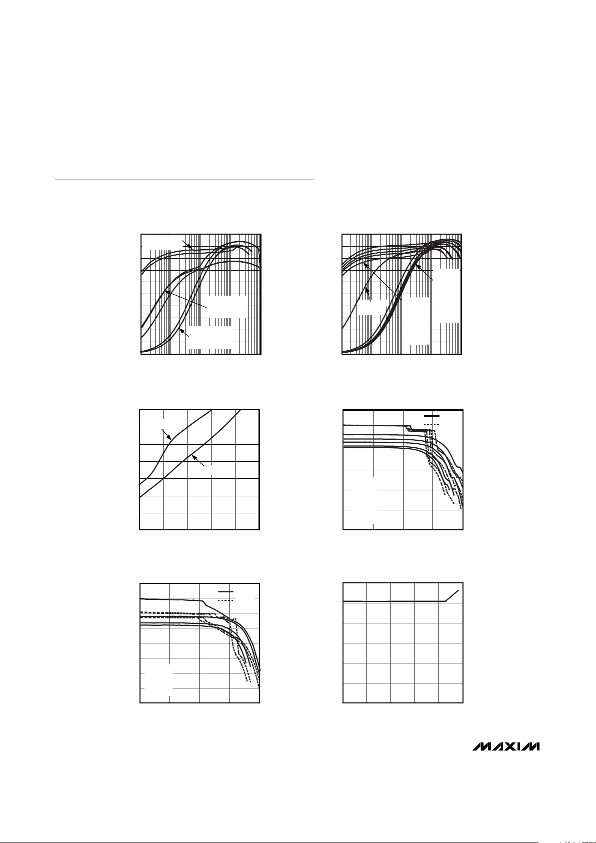
Typical Operating Characteristics
(V
OUTS
= V
POUT
= 5V, V
BATT
= VON= 3.6V, V
SKIPB
= GND.)
EFFICIENCY vs. LOAD
CURRENT, V
OUT
= 3.3V
MAX8815A toc01
OUTPUT CURRENT (mA)
EFFICIENCY (%)
100101
10
20
30
40
50
60
70
80
90
100
0
0.1 1000
VIN = 1.8V, SKIP
= 1.5V, SKIP
VIN = 3V, SKIP
= 2.5V, SKIP
= 3V, FPWM
VIN = 2.5V, SKIP
= 1.8V, SKIP
= 1.5V, FPWM
EFFICIENCY vs. LOAD
CURRENT, V
OUT
= 5V
MAX8815A toc02
OUTPUT CURRENT (mA)
EFFICIENCY (%)
100101
10
20
30
40
50
60
70
80
90
100
0
0.1 1000
VIN = 4.2V,
SKIP
SKIP
V
IN
= 3.6V,
= 3V,
= 2.4V,
= 1.8V,
= 1.5V
FPWM
V
IN
= 4.2V,
= 3.6V,
= 3V,
= 2.4V,
= 1.8V,
= 1.5V
0
0.4
0.2
0.8
0.6
1.2
1.0
1.4
1.2 2.21.7 2.7 3.2 3.7
MAXIMUM LOAD CURRENT
vs. INPUT VOLTAGE
MAX8815A toc03
INPUT VOLTAGE (V)
LOAD CURRENT (A)
V
OUT
= 5V
V
OUT
= 3.3V
4.80
4.90
4.85
5.00
4.95
5.05
5.10
0.1 101 100 1000
OUTPUT VOLTAGE
vs. LOAD CURRENT
MAX8815A toc04
LOAD CURRENT (mA)
OUTPUT VOLTAGE (V)
FPWM
SKIP
VIN = 3.6V,
= 3V,
= 2.5V,
= 1.8V,
= 1.5V
3.22
3.30
3.24
3.26
3.28
3.34
3.32
3.36
3.38
0.1 101 100 1000
OUTPUT VOLTAGE
vs. LOAD CURRENT
MAX8815A toc05
LOAD CURRENT (mA)
OUTPUT VOLTAGE (V)
VIN = 3.0V,
= 2.5V,
= 1.8V,
= 1.5V
FPWM
SKIP
0
2
1
4
3
5
6
1.2 3.22.2 4.2 5.2 6.2
OUTPUT VOLTAGE
vs. INPUT VOLTAGE
MAX8815A toc06
INPUT VOLTAGE (V)
OUTPUT VOLTAGE (V)

MAX8815A
1A, 97% Efficiency, 30µA Quiescent Current
Step-Up Converter with True Shutdown
_______________________________________________________________________________________
5
0
40
20
80
60
100
120
1.2 3.22.2 4.2 5.2 6.2
EP TEMPERATURE
vs. INPUT VOLTAGE
MAX8815A toc07
INPUT VOLTAGE (V)
EP TEMPERATURE (°C)
MEASURED AT THE BOTTOM SIDE VIA
UNDERNEATH THE EP ON THE MAX8815A
EVALUATION KIT
I
OUT
= 0.5A
I
OUT
= 1A
V
OUT
= 5V
T
A
= +25°C
0
100
50
200
150
250
300
1.2 3.22.2 4.2 5.2 6.2
INPUT CURRENT
vs. INPUT VOLTAGE, V
OUT
= 3.3V
MAX8815A toc08
INPUT VOLTAGE (V)
INPUT CURRENT (μA)
TA = -40°C
TA = +25°C
TA = +85°C
0
60
40
20
80
100
120
140
160
180
200
1.2 3.22.2 4.2 5.2 6.2
INPUT CURRENT
vs. INPUT VOLTAGE, V
OUT
= 5V
MAX8815A toc09
INPUT VOLTAGE (V)
INPUT CURRENT (μA)
TA = -40°C
TA = +25°C
TA = +85°C
0
600
400
200
800
1000
1200
1400
1600
1800
2000
1.2 3.22.2 4.2 5.2 6.2
INPUT CURRENT
vs. INPUT VOLTAGE, DURING SHUTDOWN
MAX8815A toc10
INPUT VOLTAGE (V)
INPUT CURRENT (nA)
TA = -40°C
TA = +25°C
TA = +85°C
0
400
200
800
600
1000
1200
1.2 2.41.8 3.0 3.6
STARTUP LOAD
vs. INPUT VOLTAGE
MAX8815A toc11
INPUT VOLTAGE (V)
OUTPUT CURRENT (mA)
TA = +25°C
TA = +85°C
0
1500
1000
500
2000
2500
3000
3500
4000
4500
5000
0 500
1000
1500
SOFT-START TIME
vs. LOAD CURRENT
MAX8815A toc12
LOAD CURRENT (mA)
SOFT-START TIME (μs)
Typical Operating Characteristics (continued)
(V
OUTS
= V
POUT
= 5V, V
BATT
= VON= 3.6V, V
SKIPB
= GND.)
0
200
400
600
800
1000
1200
1400
1600
1.2 2.2 3.2 4.2 5.2 6.2
SOFT-START TIME
vs. INPUT VOLTAGE
MAX8815A toc13
INPUT VOLTAGE (V)
SOFT-START TIME (μs)
MAX8815A
1A, 97% Efficiency, 30µA Quiescent Current
Step-Up Converter with True Shutdown
6 _______________________________________________________________________________________
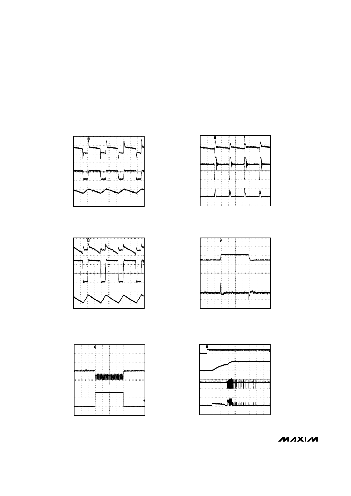
200ns/div
HEAVY-LOAD SWITCHING
WAVEFORMS
50mV/div
AC-COUPLED
V
OUT
V
LX
I
LX
MAX8815A toc14
0A
5V/div
0V
1A/div
I
OUT
= 500mA
2
μs/div
LIGHT-LOAD SWITCHING
WAVEFORMS (SKIPB = LOW)
20mV/div
AC-COUPLED
V
OUT
V
LX
I
LX
MAX8815A toc15
0A
2V/div
0V
500mA/div
I
OUT
= 10mA
200ns/div
LIGHT-LOAD SWITCHING
WAVEFORMS (SKIPB = HIGH)
20mV/div
AC-COUPLED
V
OUT
V
LX
I
LX
MAX8815A toc16
0A
2V/div
0V
500mA/div
I
OUT
= 10mA
100
μs/div
LINE TRANSIENT
20mV/div
AC-COUPLED
V
IN
V
OUT
MAX8815A toc17
2V/div
0V
3V
4.2V
3V
1ms/div
LOAD TRANSIENT
V
OUT
200mV/div
5V DC OFFSET
500mV/div
MAX8815A toc18
I
OUT
800mA
10mA
0A
200μs/div
STARTUP WAVEFORM
(NO LOAD)
V
EN
V
OUT
V
LX
I
LX
MAX8815A toc19
5V/div
5V/div
0V
5V/div
0V
1A/div
0A
Typical Operating Characteristics (continued)
(V
OUTS
= V
POUT
= 5V, V
BATT
= VON= 3.6V, V
SKIPB
= GND.)

MAX8815A
1A, 97% Efficiency, 30µA Quiescent Current
Step-Up Converter with True Shutdown
_______________________________________________________________________________________ 7
Pin Description
PIN NAME FUNCTION
1, 2 LX
Inductor Connection. LX pins are internally connected. Connect the LX pins to the switched side of
the inductor. LX is high impedance in shutdown.
3 BATT
Supply Voltage Input. Connect BATT to an input supply between 1.2V and 5V. Bypass BATT to EP
with two 4.7µF ceramic capacitors or one 10µF ceramic capacitor.
4ON
Logic On/Off Input. Drive ON low to place the MAX8815A into shutdown. During shutdown, the
control circuitry, internal switching MOSFET, and synchronous rectifier turn off and LX becomes high
impedance. Drive ON high for normal operation.
5 GND Analog Ground
6FB
Feedback Input. Connect FB to POUT to set V
OUT
= 5V. For other output voltages, connect a resistordivider from POUT to GND (see the Setting the Output Voltage section). FB regulates to 1.265V (typ)
and is high impedance in shutdown.
7 OUTS Power Bootstrapped Input. Connect OUTS to POUT through an RC filter.
8 SKIPB
PWM Mode Selection Input. Drive SKIPB low to select the normal mode of operation. Normal mode is
fixed PWM at medium to heavy loads and skip mode at light loads. Drive SKIPB high to select the
forced-PWM mode of operation.
9, 10 POUT Converter Output. Bypass POUT to EP with one 22µF tantalum capacitor.
—EP
Exposed Paddle. Connect to the ground plane to optimize thermal performance. EP is internally
connected to GND. EP must be connected to GND at a single point with a star ground connection.

MAX8815A
1A, 97% Efficiency, 30µA Quiescent Current
Step-Up Converter with True Shutdown
8 _______________________________________________________________________________________
Detailed Description
The MAX8815A current-mode step-up DC-DC switching
converter uses a fixed-frequency PWM architecture with
True Shutdown. In normal mode, the converter switches
when needed, consuming only 30µA of quiescent current. In forced-PWM mode (FPWM), the converter
switches every cycle at a constant frequency, thus
enabling noise filtering. The MAX8815A is highly efficient, with an internal switch and synchronous rectifier.
Shutdown reduces the quiescent current to less than
0.1µA. Low quiescent current and high efficiency make
this device ideal for powering portable equipment.
The MAX8815A step-up DC-DC switching converter typically generates a 3.3V to 5V output voltage from a 1.2V
to 5.5V battery input voltage. The converter operates in
bootstrapped mode with the output powering the device
once the output voltage is ≥ 3V. The current limit is set at
2.5A to deliver 1A at 5V from a 2.5V input, or 500mA at
5V using a 2-cell 1.8V input. Internal soft-start limits the
inrush current to less than 500mA under no-load conditions during startup.
The MAX8815A switches at a 2MHz frequency, allowing for tiny external components. Internal compensation
further reduces the external component count in cost
and space-sensitive applications. The MAX8815A is
optimized for use in DSC and other applications requiring low quiescent current for maximum battery life.
Figures 1a and 1b show the typical application circuits.
ON
SKIPB
POUT
BATT
LX
FB
OUTS
GND
ON
ON
3V
ON
ON
PGND
CONTROL
2MHz
OSCILLATOR
REFERENCE
EP
+
-
STARTUP
OSCILLATOR
MAX8815A
Functional Diagram

MAX8815A
1A, 97% Efficiency, 30µA Quiescent Current
Step-Up Converter with True Shutdown
_______________________________________________________________________________________ 9
1a. FIXED 5V OUTPUT
BATT
ON
SKIPB
LX
POUT
OUTS
FB
GND
INPUT VOLTAGE
1.2V TO 5.5V
3
L
2μH
1, 2
5
MAX8815A
OUTPUT VOLTAGE
5V; UP TO 1A
9, 10
R3
100kΩ
C3
0.1μF
C2
22μF
7
6
8
4
ON
OFF
FPWM
NORM
C1
10μF
BATT
ON
SKIPB
LX
POUT
OUTS
FB
OUTPUT VOLTAGE
3.3V TO 5V; UP TO 1A
INPUT VOLTAGE
1.2V TO 5.5V
8
4
3
L
2μH
1, 2
9, 10
MAX8815A
ON
OFF
FPWM
NORM
C1
10μF
GND
R1
R2
R3
100kΩ
C2
22μF
C3
0.1μF
7
6
5
1b. ADJUSTABLE OUTPUT VOLTAGE
Figure 1. Typical Application Circuits

MAX8815A
DC-DC Converter
The MAX8815A uses a current-mode PWM control
scheme. The voltage difference between FB and an
internal 1.265V (typ) reference generates an error signal that programs the peak inductor current to regulate
the output voltage. The default peak-inductor current
limit is 2.5A (typ). Inductor current is sensed across the
internal switch and summed with a slope-compensation
signal. The PWM comparator compares this summed
signal to the error-amplifier output. At the beginning of
each clock cycle, the n-channel switch turns on until
the PWM comparator trips. During this time, inductor
current ramps up, storing energy in its magnetic field.
When the n-channel switch turns off, the internal synchronous p-channel rectifier turns on. The inductor
releases the stored energy as the current ramps down
and provides energy to the output. The MAX8815A
operates in two modes, normal mode and FPWM mode,
depending on the voltage at SKIPB.
Normal Mode
Drive SKIPB low to select the normal mode of operation. In this mode, the device operates in PWM only
when driving medium to heavy loads. As the load current decreases and crosses the low-power idle-mode
threshold, the PWM comparator and oscillator are disabled. In this low-power mode, switching occurs only
as needed to service the output. This improves the efficiency for light loads, and the device consumes only
30µA under no-load conditions. The threshold for entering skip mode is approximately 90mA load with a 3.6V
input and 5V output. When switching in normal mode,
the inductor current terminates at zero for each switching cycle.
FPWM Mode
Drive SKIPB high to select the MAX8815A’s FPWM
mode of operation. The IC switches at a constant frequency (2MHz) and modulates the MOSFET switch
pulse width to control the power transferred per cycle
to regulate the output voltage. Switching harmonics
generated by fixed-frequency operation are consistent
and easily filtered. This is important in noise-sensitive
applications.
The MAX8815A does not allow for dynamic switching
between normal and FPWM modes.
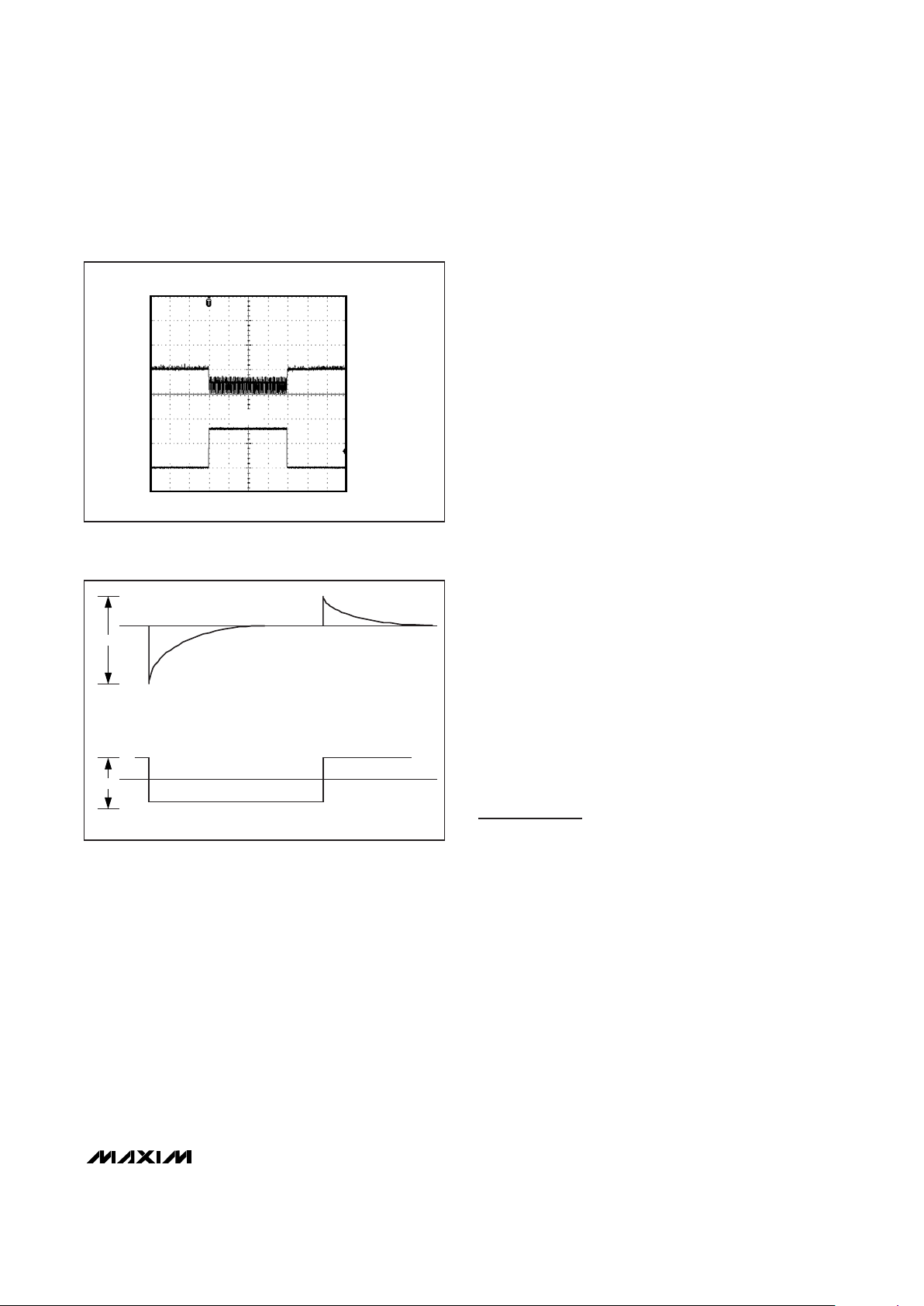
Load-Transient Response/
Voltage Positioning
The MAX8815A matches the load regulation to the voltage droop seen during load transients. This is sometimes called voltage positioning. Benefits include lower
peak-to-peak output-voltage deviation for a given load
step without requiring an increase in filter load capacitance. There is minimal voltage droop when transitioning from light load to full load and minimum overshoot
when going from full load to light load.
The term “positioning” refers to setting the output voltage to a level that is dependent on load current (Figure
2). At minimum load, the output voltage is set to a
slightly higher than nominal level. At full load, the output
voltage is slightly lower than the nominal level. With
voltage positioning, the total voltage deviation during a
transient is significantly improved over traditional highgain control loops. Traditional high-gain loops use integrators that maximize gain at low frequencies to
provide tight DC-load regulation; however, due to the
capacitive element in the feedback loop, these highgain amplifiers typically take hundreds of microseconds to respond to a load step and return to steady
state. As a result, the voltage can droop by as much as
6% or more during the recovery time. In portable equipment where the output load can change frequently and
the amount of output capacitance is limited, this can
result in a wide short-term output fluctuation (Figure 3).
Voltage positioning on the MAX8815A allows up to 3%
(typ) of load regulation and no further transient droop
(Figures 2 and 3). Thus, during load transients the voltage delivered remains within specification more effectively than other regulators that might have tighter DC
accuracy. In systems with high-speed CPUs, thousands of system clock cycles can occur during the time
it takes a traditional high-gain loop to respond to a load
step. Consequently, 3% load regulation with no transient droop is better suited to such systems than a
power supply that may specify 1% DC-load regulation,
but then exhibits 6% or more of transient droop during
load steps (see the Load Transient graph in the
Typical
Operating Characteristics
section).
1A, 97% Efficiency, 30µA Quiescent Current
Step-Up Converter with True Shutdown
10 ______________________________________________________________________________________
True Shutdown
Drive ON low to place the MAX8815A in shutdown mode
and reduce supply current to 0.1µA (typ).
In shutdown, the control circuitry, internal switching
MOSFET, and synchronous rectifier turn off and LX
becomes high impedance. Drive ON high for normal
operation. The internal synchronous rectifier allows for
conversion efficiencies as high as 97%. In conventional
step-up circuits, the body diode of the synchronous rectifier is forward biased in shutdown and allows current
flow from the battery to the output. If the load cannot be
shut down, an external switch is required to avoid depleting the battery during shutdown. A proprietary design in
the MAX8815A allows the synchronous rectifier to provide True Shutdown with no additional components. This
allows the output to fall to GND in shutdown and
removes any connection between the input and output.
Soft-Start
The MAX8815A has internal soft-start circuitry that controls inrush current at startup, reducing transients on
the input source. Soft-start is particularly useful for
higher impedance input sources, such as Li+ and alkaline cells. The soft-start duration is proportional to the
size of the output capacitor and load resistance. See
the
Typical Operating Characteristics
section for plots
of Soft-Start Time vs. Load Current and Soft-Start Time
vs. Input Voltage.
Fault Protection
The MAX8815A has robust fault and overload protection. After power-up, the device monitors for an out-ofregulation state such as an overload or short-circuit
condition. If the converter remains faulted for 16ms, the
output latches off until the part is reinitialized by toggling ON or cycling power to the IC. If the output falls
10% below its regulation voltage or is shorted, the
device enters the fault state immediately.
If the short exists on the output before the IC is powered up, the converter goes through soft-start once and
then latches off (6ms) because the output never reaches regulation. The part draws about 1A of input current
during the startup period. Limiting the time under this
condition prevents thermal runaway.
Applications Information
Setting the Output Voltage
The MAX8815A has a preset output voltage of 5V. To set
other output voltages, use external feedback resistors.
To set the output voltage between 3.3V and 5V, connect FB to the center of an external resistor voltagedivider between POUT and GND, as shown in Figure
1b. Select the value of R2 no more than 500kΩ, and
then calculate the value for R1 as follows:
R1 = R2 (V
OUT/VFB
- 1)
where VFBis the FB regulation voltage, 1.265V (typ).
MAX8815A
1A, 97% Efficiency, 30µA Quiescent Current
Step-Up Converter with True Shutdown
______________________________________________________________________________________ 11
(a) HIGH-GAIN DC LOAD REGULATION WITH POOR TRANSIENT RESPONSE
(b) VOLTAGE POSITIONING WITH DC LOAD REGULATION
9%
3%
Figure 3. Transient-Response Comparison
1ms/div
LOAD TRANSIENT
V
OUT
200mV/div
5V DC OFFSET
500mV/div
MAX8815A toc18
I
OUT
800mA
10mA
0A
Figure 2. Load Regulation

MAX8815A
1A, 97% Efficiency, 30µA Quiescent Current
Step-Up Converter with True Shutdown
Inductor Selection
In most step-up converter designs, a reasonable inductor value can be derived from the following equation.
This equation sets peak-to-peak inductor current at 1/2
the DC inductor current:
L = (2 x V
BATT
x D x (1 - D))/(I
OUT(MAX)
x fSW)
where f
SW
is the switching frequency (2MHz), and D is
the duty factor given by D = 1 - (V
BATT/VOUT
). Using L
from the equation above results in a peak-to-peak
inductor current ripple of 0.5 x I
OUT
/(1 - D), and a peak
inductor current of 1.25 x I
OUT
/(1 - D). Ensure that the
peak (saturation) current rating of the inductor meets or
exceeds this requirement. The recommended inductance range for the MAX8815A is 1µH to 2.2µH. See
Table 1 for recommended inductors.
Capacitor Selection
Output Capacitor
Output capacitor C2 in Figures 1a and 1b is required to
keep the output voltage ripple small and to ensure regulation loop stability. The output capacitors must have
low impedance at the switching frequency. Make sure
the output capacitors maintain their capacitance over
DC bias and the desired operating temperature range.
One 22µF tantalum capacitor is recommended.
Input Capacitor
Input capacitor C1 reduces the current peaks drawn
from the battery or input power source and reduce
switching noise in the IC. The impedance of the input
capacitor at the switching frequency should be kept
very low. A ceramic capacitor is highly recommended
due to their small size and low ESR. Make sure the
input capacitors maintain their capacitance over DC
bias and the desired operating temperature range.
Ceramic capacitors with X5R or X7R dielectric temperature characteristics generally perform well. Two 4.7µF
or one 10µF ceramic capacitors are recommended.
PCB Layout and Routing
Good printed-circuit board (PCB) layout is important to
achieve optimal performance for the MAX8815A. Poor
design can cause excessive conducted and radiated
noise. Conductors carrying discontinuous currents and
any high-current path should be made as short and
wide as possible. Keep the feedback network (R1 and
R2) very close to the IC, preferably within 0.2in of the
FB and GND pins. Nodes with high dV/dt (switching
nodes) should be kept as small as possible and routed
away from FB. Connect the input and output capacitors
as close as possible to the IC. Refer to the MAX8815A
EV kit data sheet for a PCB layout example.
Chip Information
PROCESS: BiCMOS
INDUCTOR
L
(µH)
DCR
(mΩ)
I
SAT
(A)
SIZE (mm)
TOKO DE4012CK
A1101AS-1R0M
1 45 3.3 4 x 4 x 1.2
TOKO DE4012CK
A1101AS-2R2M
2.2 60 2.8 4 x 4 x 1.2
TOKO 2818C
1072AS-1R0M
1 40 2.8 2.8 x 2.8 x 1.8
Table 1. Recommended Inductors
PACKAGE TYPE PACKAGE CODE DOCUMENT NO.
10 TDFN-EP T1033-2
21-0137
Package Information
For the latest package outline information, go to
www.maxim-ic.com/packages
.
Maxim cannot assume responsibility for use of any circuitry other than circuitry entirely embodied in a Maxim product. No circuit patent licenses are
implied. Maxim reserves the right to change the circuitry and specifications without notice at any time.
12
____________________Maxim Integrated Products, 120 San Gabriel Drive, Sunnyvale, CA 94086 408-737-7600
© 2008 Maxim Integrated Products is a registered trademark of Maxim Integrated Products, Inc.
 Loading...