General Description
The MAX8815A DC-DC step-up converter is a high-efficiency, low quiescent current, synchronous step-up
converter with True Shutdown™ and inrush-current limiting. The MAX8815A generates any output voltage
from 3.3V to 5V from a 2-cell NiMH/NiCd or a single-cell
Li+/Li polymer battery.
The MAX8815A uses two modes of operation. The first
mode of operation (normal) uses only 30µA (typ) quiescent current and allows the converter to switch only
when needed at no load and light loads. Under moderate and heavy loads (typically above 90mA), the
MAX8815A uses a fixed-frequency pulse-width modulation (PWM) technique. This mode allows maximum efficiency at light loads. The second mode of operation is
a fixed-frequency forced-pulse-width modulation
(FPWM) mode where the converter switches at a fixed
frequency irrespective of the load. This mode allows for
easy noise filtering and lower output ripple.
The MAX8815A has a preset 2.5A current limit, allowing
500mA load at 1.8V input and 1A load at 2.5V input when
the output is set to 5V. Features include soft-start, which
limits inrush current during startup, True Shutdown, and
internal compensation. The MAX8815A is available in a
compact 10-pin, 3mm x 3mm TDFN package.
The MAX8815A evaluation kit can help shorten the time
required for system design.
Applications
DSC and DVC
Microprocessor/DSP Core Power
Cell Phones, PDAs, MP3 Players
Portable Handheld Devices
PCMCIA Cards
Features
♦ Up to 97% Efficiency with Internal Synchronous
Rectifier
♦ Low 30µA Quiescent Current
♦ Guaranteed 500mA Output Current at V
OUT
= 5V
from 1.8V Input
♦ Guaranteed 1A Output Current at 5V from 2.5V
Input
♦ Low-Noise Constant Frequency Operation (FPWM
Mode)
♦ 2MHz PWM Switching Frequency
♦ Preset (5V) or Adjustable Output
♦ Controlled Current in Soft-Start Limits Inrush
Current
♦ True Shutdown
♦ Internal Compensation
♦ Overload/Short-Circuit Protection
♦ 0.1µA Shutdown Current
♦ Thermal Shutdown
♦ Compact 10-Pin, 3mm x 3mm TDFN Package
MAX8815A
1A, 97% Efficiency, 30µA Quiescent Current
Step-Up Converter with True Shutdown
________________________________________________________________
Maxim Integrated Products
1
Ordering Information
19-4092; Rev 0; 5/08
For pricing, delivery, and ordering information, please contact Maxim Direct at 1-888-629-4642,
or visit Maxim’s website at www.maxim-ic.com.
EVALUATION KIT
AVAILABLE
PART PIN-PACKAGE TOP MARK
MAX8815AETB+ 10 TDFN-EP* AUH
True Shutdown is a trademark of Maxim Integrated Products, Inc.
+
Denotes a lead-free package.
*
EP = Exposed pad.
Note: This device operates in the -40°C to +85°C extended
operating temperature range.
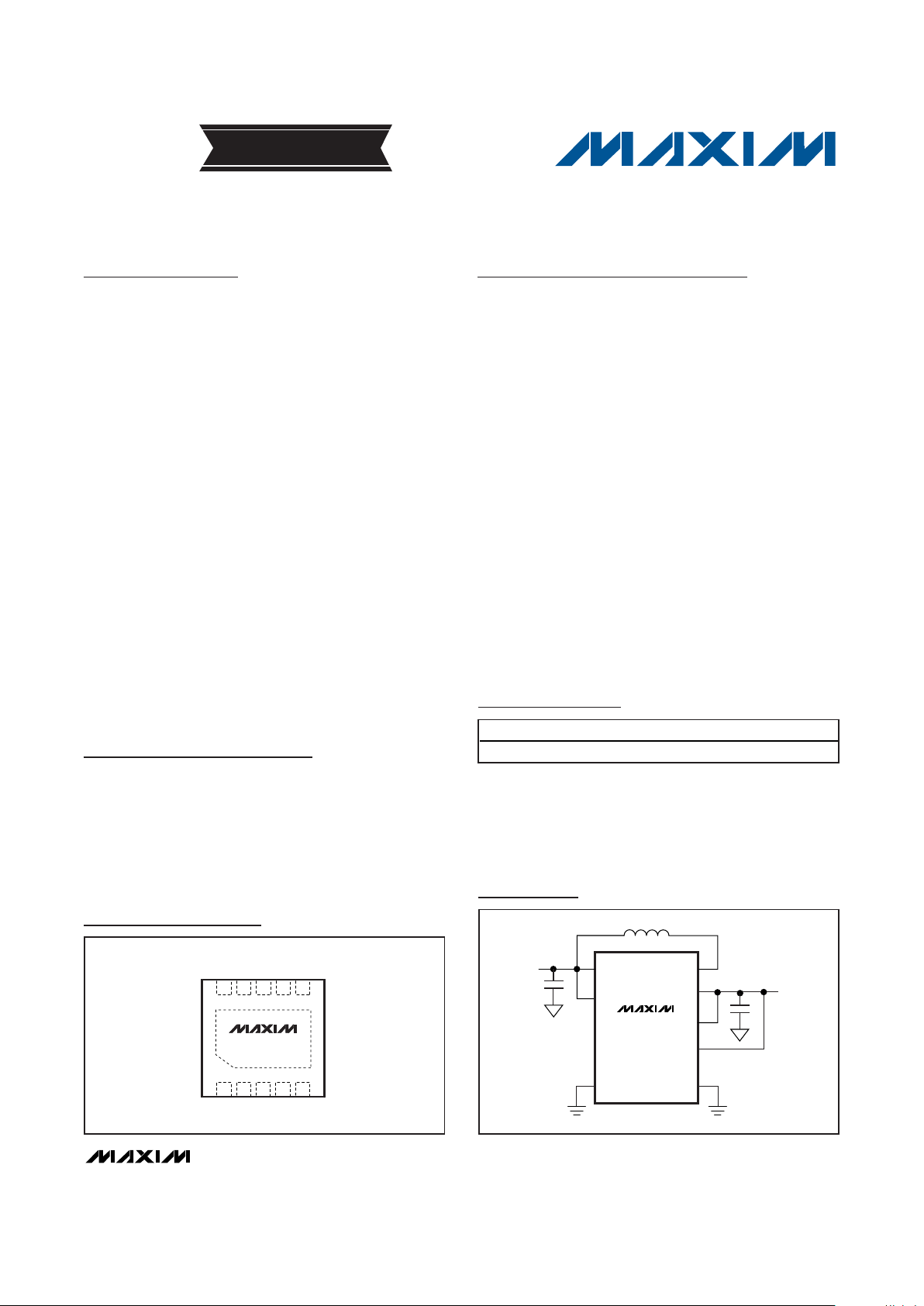
BATT
ON
SKIPB
LX
POUT
OUTS
FB
GND
INPUT VOLTAGE
1.2V TO 5.5V
OUTPUT VOLTAGE
5V UP TO 1A
MAX8815A
Typical Operating Circuit
TOP VIEW
SKIPB
OUTS
FB
ON
GND
1
2
3
4
5
10
98
7
6
POUT
POUT
LX
BATT
LX
MAX8815A
+
Pin Configuration

MAX8815A
1A, 97% Efficiency, 30µA Quiescent Current
Step-Up Converter with True Shutdown
2 _______________________________________________________________________________________
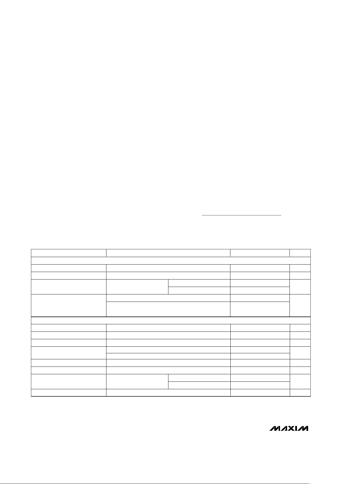
ELECTRICAL CHARACTERISTICS
(V
OUTS
= V
POUT
= 5V, VON= V
BATT
= 3.6V, V
SKIPB
= GND, TA= -40°C to +85°C, typical values are at TA= +25°C, unless otherwise
noted. Limits are 100% production tested at T
A
= +25°C. Limits over the operating temperature range are guaranteed by design and
characterization.)
Stresses beyond those listed under “Absolute Maximum Ratings” may cause permanent damage to the device. These are stress ratings only, and functional
operation of the device at these or any other conditions beyond those indicated in the operational sections of the specifications is not implied. Exposure to
absolute maximum rating conditions for extended periods may affect device reliability.
PARAMETER CONDITIONS MIN TYP MAX UNITS
GENERAL
Operating Input Voltage Range 1.2 5.5 V
Minimum Startup Voltage 1.2 1.5 V
TA = +25°C 0.1 1
Shutdown Supply Current ON = GND
T
A
= +85°C 0.2
µA
No load, no switching, VFB = 1.28V 16 30
Supply Current
No load, switching (measured with external feedback);
V
POUT
= 5V
30
µA
OSCILLATOR
Switching Frequency 1.8 2.0 2.2 MHz
Maximum Duty Cycle 87.5 %
Output-Voltage Adjust Range 3.3 5.0 V
No load, TA = +25°C 1.255 1.265 1.275
FB Regulation Voltage
No load, T
A
= -40°C to +85°C (Note 3) 1.252 1.265 1.277
V
FB Load Regulation -7.5 mV/A
FB Line Regulation V
BATT
= 1.8V to 5V, I
POUT
= 0.5A -10 mV/D
TA =+25°C -50 -5 +50
FB Input Leakage Current
V
FB
= 1.28V, V
OUTS
=
V
POUT
= V
BATT
= 5.5V
T
A
= +85°C -5
nA
Idle Mode™ Trip Level (Note 4) 90 mA
ABSOLUTE MAXIMUM RATINGS
OUTS, BATT to GND ................................................-0.3V to +6V
POUT to OUTS ......................................................-0.3V to +0.3V
PGND (EP) to AGND .............................................-0.3V to +0.3V
FB to GND ................................................-0.3V to (V
OUT
+ 0.3V)
ON, SKIPB to GND ............-0.3V to the higher of (V
OUTS
+ 0.3V)
and (V
BATT
+ 0.3V)
LX Continuous Current (Note 1)..........................................2.75A
Continuous Power Dissipation (T
A
= +70°C)
10-Pin TDFN Single-Layer Board (derate 18.5 mW/°C
above +70°C)...........................................................1481.5mW
10-Pin TDFN Multilayer Board (derate 24.4 mW/°C
above +70°C)...........................................................1951.2mW
Junction-to-Case Thermal Resistance (θ
JC
) (Note 2)
10-Pin TDFN.................................................................8.5°C/W
Junction-to-Ambient Thermal Resistance (θ
JA
) (Note 2)
10-Pin TDFN..................................................................41°C/W
Operating Temperature Range ...........................-40°C to +85°C
Junction Temperature Range ............................-40°C to +150°C
Storage Temperature Range .............................-65°C to +150°C
Lead Temperature (soldering, 10s) .................................+300°C
Note 1: LX has internal clamp diodes to PGND (EP) and VPWR, where VPWR is the internal power node and is the higher of BATT
and OUTS. Applications that forward bias these diodes should take care not to exceed the power-dissipation limits of the
device.
Note 2: Package thermal resistances were obtained using the method described in JEDEC specification JESD51-7, using a 4-layer
board. For detailed information on package thermal considerations, visit www.maxim-ic.com/thermal-tutorial
.
Idle Mode is a trademark of Maxim Integrated Products, Inc.

MAX8815A
1A, 97% Efficiency, 30µA Quiescent Current
Step-Up Converter with True Shutdown
_______________________________________________________________________________________ 3
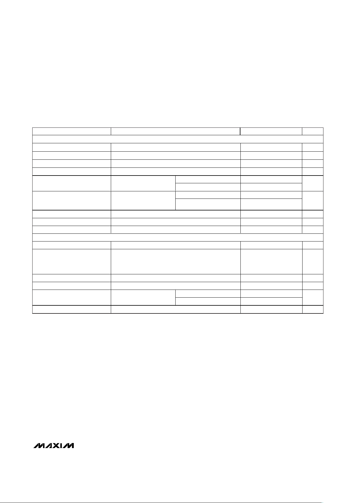
PARAMETER CONDITIONS MIN TYP MAX UNITS
DC-DC SWITCHES
p-Channel On-Resistance 0.14 0.25 Ω
n-Channel On-Resistance 0.1 0.17 Ω
n-Channel Current Limit 2.20 2.5 2.75 A
p-Channel Turn-Off Current 10 mA
TA = +25°C 0.1 2
OUT Leakage Current
V
LX
= VON = 0V, V
OUTS
=
V
POUT
= V
BATT
= 5.5V
T
A
= +85°C 0.2
µA
TA = +25°C 0.1 2
LX Leakage Current
V
LX
= 0V or 5.5V, V
OUTS
=
V
POUT
= V
BATT
= 5.5V,
V
ON
= 0V
T
A
= +85°C 0.2
µA
Soft-Start Interval Load dependent 6 ms
Overload Protection Fault Delay 16 ms
Startup into a Short Circuit 6ms
LOGIC INPUTS
ON Input Low Level V
OUTS
= V
POUT
= 0V and 1.5V < V
BATT
< 5.5V 0.5 V
ON Input High Level
V
OUTS
= V
POUT
= 0V and 1.5V < V
BATT
< 5.5V, VH is the
highter of V
POUT
and V
BATT
VH -
0.2V
(1.3V
max
)
V
SKIPB Input Low Level 3.3V < V
POUT
< V
OUT
< 5.5V 0.5 V
SKIPB Input High Level 3.3V < V
POUT
< V
OUT
< 5.5V 1.6 V
TA = +25°C 0.01 1
ON, SKIPB Input Leakage
Current
V
OUTS
= V
POUT
= V
BATT
=
5.5V
T
A
= +85°C 0.02
µA
Thermal Shutdown +167 °C
ELECTRICAL CHARACTERISTICS (continued)
(V
OUTS
= V
POUT
= 5V, VON= V
BATT
= 3.6V, V
SKIPB
= GND, TA= -40°C to +85°C, typical values are at TA= +25°C, unless otherwise
noted. Limits are 100% production tested at T
A
= +25°C. Limits over the operating temperature range are guaranteed by design and
characterization.)
Note 3: Guaranteed by design. Not production tested.
Note 4: The idle-mode current threshold is the transition point between fixed-frequency PWM operation and idle-mode operation. The
specification is given in terms of output load current for inductor values shown in the typical application circuits (Figure 1). The
idle-mode transition varies with input-to-output voltage ratio.

MAX8815A
1A, 97% Efficiency, 30µA Quiescent Current
Step-Up Converter with True Shutdown
4 _______________________________________________________________________________________
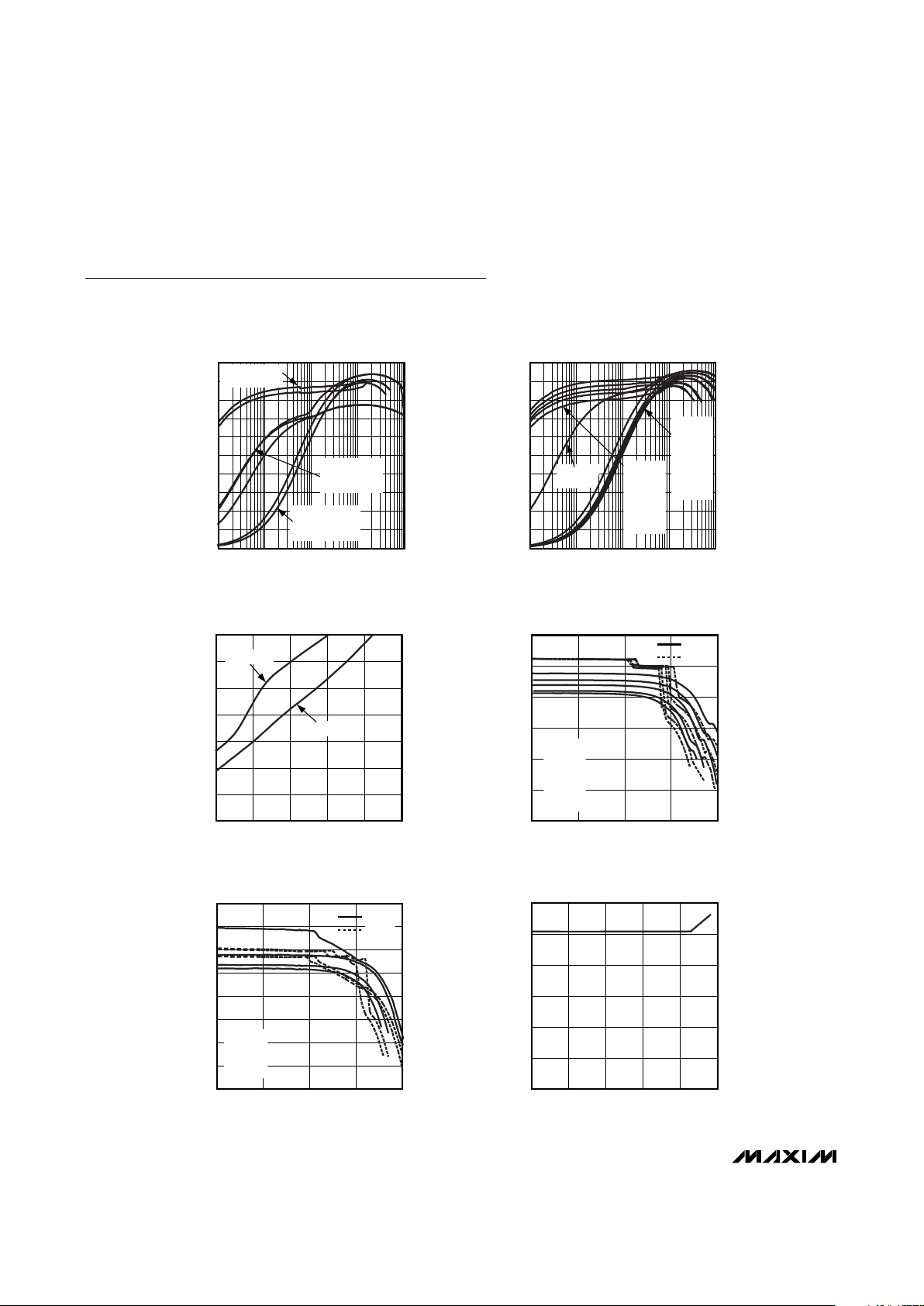
Typical Operating Characteristics
(V
OUTS
= V
POUT
= 5V, V
BATT
= VON= 3.6V, V
SKIPB
= GND.)
EFFICIENCY vs. LOAD
CURRENT, V
OUT
= 3.3V
MAX8815A toc01
OUTPUT CURRENT (mA)
EFFICIENCY (%)
100101
10
20
30
40
50
60
70
80
90
100
0
0.1 1000
VIN = 1.8V, SKIP
= 1.5V, SKIP
VIN = 3V, SKIP
= 2.5V, SKIP
= 3V, FPWM
VIN = 2.5V, SKIP
= 1.8V, SKIP
= 1.5V, FPWM
EFFICIENCY vs. LOAD
CURRENT, V
OUT
= 5V
MAX8815A toc02
OUTPUT CURRENT (mA)
EFFICIENCY (%)
100101
10
20
30
40
50
60
70
80
90
100
0
0.1 1000
VIN = 4.2V,
SKIP
SKIP
V
IN
= 3.6V,
= 3V,
= 2.4V,
= 1.8V,
= 1.5V
FPWM
V
IN
= 4.2V,
= 3.6V,
= 3V,
= 2.4V,
= 1.8V,
= 1.5V
0
0.4
0.2
0.8
0.6
1.2
1.0
1.4
1.2 2.21.7 2.7 3.2 3.7
MAXIMUM LOAD CURRENT
vs. INPUT VOLTAGE
MAX8815A toc03
INPUT VOLTAGE (V)
LOAD CURRENT (A)
V
OUT
= 5V
V
OUT
= 3.3V
4.80
4.90
4.85
5.00
4.95
5.05
5.10
0.1 101 100 1000
OUTPUT VOLTAGE
vs. LOAD CURRENT
MAX8815A toc04
LOAD CURRENT (mA)
OUTPUT VOLTAGE (V)
FPWM
SKIP
VIN = 3.6V,
= 3V,
= 2.5V,
= 1.8V,
= 1.5V
3.22
3.30
3.24
3.26
3.28
3.34
3.32
3.36
3.38
0.1 101 100 1000
OUTPUT VOLTAGE
vs. LOAD CURRENT
MAX8815A toc05
LOAD CURRENT (mA)
OUTPUT VOLTAGE (V)
VIN = 3.0V,
= 2.5V,
= 1.8V,
= 1.5V
FPWM
SKIP
0
2
1
4
3
5
6
1.2 3.22.2 4.2 5.2 6.2
OUTPUT VOLTAGE
vs. INPUT VOLTAGE
MAX8815A toc06
INPUT VOLTAGE (V)
OUTPUT VOLTAGE (V)
 Loading...