

General Description
The MAX8814 intelligent, stand-alone constant-current,
constant-voltage (CCCV), thermally regulated linear
charger is designed for charging a single-cell lithiumion (Li+) battery. The MAX8814 integrates the currentsense circuit, MOSFET pass element, thermalregulation circuitry, and eliminates the reverse-blocking
Schottky diode to create the simplest and smallest
charging solution for handheld equipment.
The IC controls the charging sequence from the prequalification state through constant-current fast-charge
and the final constant voltage charge. Proprietary thermal-regulation circuitry limits the die temperature during fast-charging or when the IC is exposed to high
ambient temperatures, allowing maximum charging
current without damaging the IC.
The MAX8814 achieves high flexibility by providing an
adjustable fast-charge current through an external
resistor. Other features include an active-low control
input (EN) and an active-low input power-source detection output (POK). The IC also features a booting assistant circuit that distinguishes input sources and battery
connection and provides an output signal (ABO) for
system booting.
The MAX8814 accepts an input supply range from
4.25V to 28V, but disables charging if the input voltage
exceeds +7V to protect against unqualified or faulty AC
adapters. The IC operates over the extended temperature range (-40°C to +85°C) and is available in a compact 8-pin thermally enhanced TDFN 2mm x 2mm
package (0.8mm max height).
Applications
Cellular and Cordless Phones
Smartphones and PDAs
MP3 Players
Digital Still Cameras
USB Appliances
Charging Cradles and Docks
Bluetooth
®
Equipment
Features
o CCCV, Thermally Regulated Linear 1-Cell Li+
Battery Charger
o No External MOSFET, Reverse Blocking Diode, or
Current-Sense Resistor
o Programmable Fast-Charge Current (1A
RMS
max)
o Proprietary Die Temperature Regulation Control
(+115°C)
o 4.25V to 28V Input Voltage Range with Input OVP
Above +7V
o Charge-Current Monitor for Fuel Gauging (ISET)
o Low Dropout Voltage (300mV at 500mA)
o Input Power-Source Detection Output (POK),
Charge-Enable Input (EN)
o Soft-Start Limits Inrush Current
o Output for Autobooting (ABO)
o Tiny 2mm x 2mm, 8-Pin TDFN Package, 0.8mm
Height (max)
MAX8814
28V Linear Li+ Battery Charger with
Smart Autoboot Assistant
________________________________________________________________
Maxim Integrated Products
1
19-0994; Rev 0; 10/07
For pricing, delivery, and ordering information, please contact Maxim Direct at 1-888-629-4642,
or visit Maxim's website at www.maxim-ic.com.
EVALUATION KIT
AVAILABLE
Ordering Information
IN
EN
ABI
ISET
GND
ABO
BATT
EP
ON
OFF
POK
SYSTEM
SUPPLY
2.2μF Li+
4.25V TO 28V
MAX8814
+
Typical Operating Circuit
PART
TEMP
RANGE
PINPACKAGE
PKG
CODE
TOP
MARK
MAX8814ETA+
-40°C to
+85°C
8 TDFN
2mm x 2mm
T822+2 ABI
Bluetooth is a registered trademark of Bluetooth SIG.
+
Denotes a lead-free and RoHS-compliant package.
Pin Configuration appears at end of data sheet.
MAX8814
28V Linear Li+ Battery Charger with
Smart Autoboot Assistant
2 _______________________________________________________________________________________
ABSOLUTE MAXIMUM RATINGS
ELECTRICAL CHARACTERISTICS
(VIN= 5V, V
BATT
= 4V, R
POK
= 1MΩ to BATT, EN = 0V, R
ISET
= 2.8kΩ to GND, C
BATT
= 2.2µF, TA= -40°C to +85°C, unless other-
wise noted. Typical values are at T
A
= +25°C.) (Note 1)
Stresses beyond those listed under “Absolute Maximum Ratings” may cause permanent damage to the device. These are stress ratings only, and functional
operation of the device at these or any other conditions beyond those indicated in the operational sections of the specifications is not implied. Exposure to
absolute maximum rating conditions for extended periods may affect device reliability.
IN to GND ...............................................................-0.3V to +30V
ABI, BATT, EN, POK to GND....................................-0.3V to +6V
ABO to GND............................................-0.3V to (V
BATT
+ 0.3V)
ISET to GND .............................................................-0.3V to +4V
IN to BATT Continuous Current .........................................1A
RMS
Continuous Power Dissipation (TA= +70°C)
8-Pin TDFN (derate 11.9mW/°C above +70°C)
(multilayer PCB) ........................................................953.5mW
BATT Short-Circuit Duration .......................................Continuous
Operating Temperature Range ...........................-40°C to +85°C
Junction Temperature......................................................+150°C
Storage Temperature Range .............................-65°C to +150°C
Lead Temperature (soldering, 10s) .................................+300°C
PARAMETER CONDITIONS MIN TYP MAX UNITS
Input Voltage Range 028V
Input Operating Voltage Range 4.25 6.50 V
VIN rising 40
Power-OK Threshold
V
IN
- V
BATT
,
10mV hysteresis (typ)
V
IN
falling 30
mV
Overvoltage-Lockout Trip
Threshold
V
IN
rising, 100mV hysteresis (typ) 6.5 7 7.5 V
Constant-current charging mode (I
BATT
= 0A) 0.8 1.35
IC disabled (VEN = 5V) 0.23 0.50
TA = +25°C 0.021 0.065
IN Input Current
V
IN
= 4V,
V
BATT
= 4.2V
T
A
= +85°C 0.021
mA
VIN = 0 to 4V,
V
BATT
= 4.2V
110
BATT Input Current
IC disabled 3
µA
T
A
= 0°C to +85°C 4.179 4.200 4.221
Battery Regulation Voltage I
BATT
= 0A
T
A
= -40°C to +85°C 4.158 4.200 4.242
V
Minimum BATT Bypass
Capacitance
2.2 µF
T
A
= 0°C to +85°C 524 570 616
V
BATT
= 3.5V
T
A
= -40°C to +85°C 485 570 656
T
A
= 0°C to +85°C 89 107 125
Fast-Charge Current
V
BATT
= 3.5V,
R
ISET
= 14kΩ
T
A
= -40°C to +85°C 80 107 134
mA
Prequalification Charge Current
Percentage of the fast-charge current, V
BATT
= 2.2V,
T
A
= 0°C to +85°C
41015%
Die Temperature Regulation
Threshold
+115 °C
V
BATT
Prequalification Threshold
Voltage
V
BATT
rising, 100mV hysteresis (typ) 2.3 2.5 2.7 V
Current-Sense Amplifier Gain
(I
BATT
to I
ISET
)
I
BATT
= 570mA 877.2 µA/A
MAX8814
28V Linear Li+ Battery Charger with
Smart Autoboot Assistant
_______________________________________________________________________________________ 3
PARAMETER CONDITIONS MIN TYP MAX UNITS
Regulator Dropout Voltage
(V
IN
- V
BATT
)
V
BATT
= 4.1V, I
BATT
= 425mA 240 500 mV
EN Logic-Input Low Voltage 4.25V < VIN < 6.5V 0.4 V
EN Logic-Input High Voltage 4.25V < VIN < 6.5V 1.3 V
EN and ABI Internal Pulldown
Resistance
100 200 400 kΩ
ABI Logic-Input Low Voltage VIN = 0V 0.4 V
ABI Logic-Input High Voltage VIN = 0V 1.3 V
ABO Output Low Voltage I
ABO (SINK)
= 1mA 0.4 V
ABO Output High Voltage I
ABO (SOURCE)
= 1mA
V
BATT
-
0.4V
V
POK Output Low Voltage I
POK
= 5mA 0.4 V
TA = +25°C 0.001 1
POK Output High Leakage
Current
V
POK
= 5.5V
T
A
= +85°C 0.002
µA
ELECTRICAL CHARACTERISTICS (continued)
(VIN= 5V, V
BATT
= 4V, R
POK
= 1MΩ to BATT, EN = 0V, R
ISET
= 2.8kΩ to GND, C
BATT
= 2.2µF, TA= -40°C to +85°C, unless other-
wise noted. Typical values are at T
A
= +25°C.) (Note 1)
Note 1: Specifications are 100% production tested at TA= +25°C. Limits over the operating temperature range are guaranteed by
design and characterization.
Typical Operating Characteristics
(VIN= 5V, V
BATT
= 4V, R
POK
= 1MΩ to BATT, EN = 0V, R
ISET
= 2.8kΩ to GND, C
BATT
= 2.2µF, TA= -40°C to +85°C, unless other-
wise noted. Typical values are at T
A
= +25°C.)
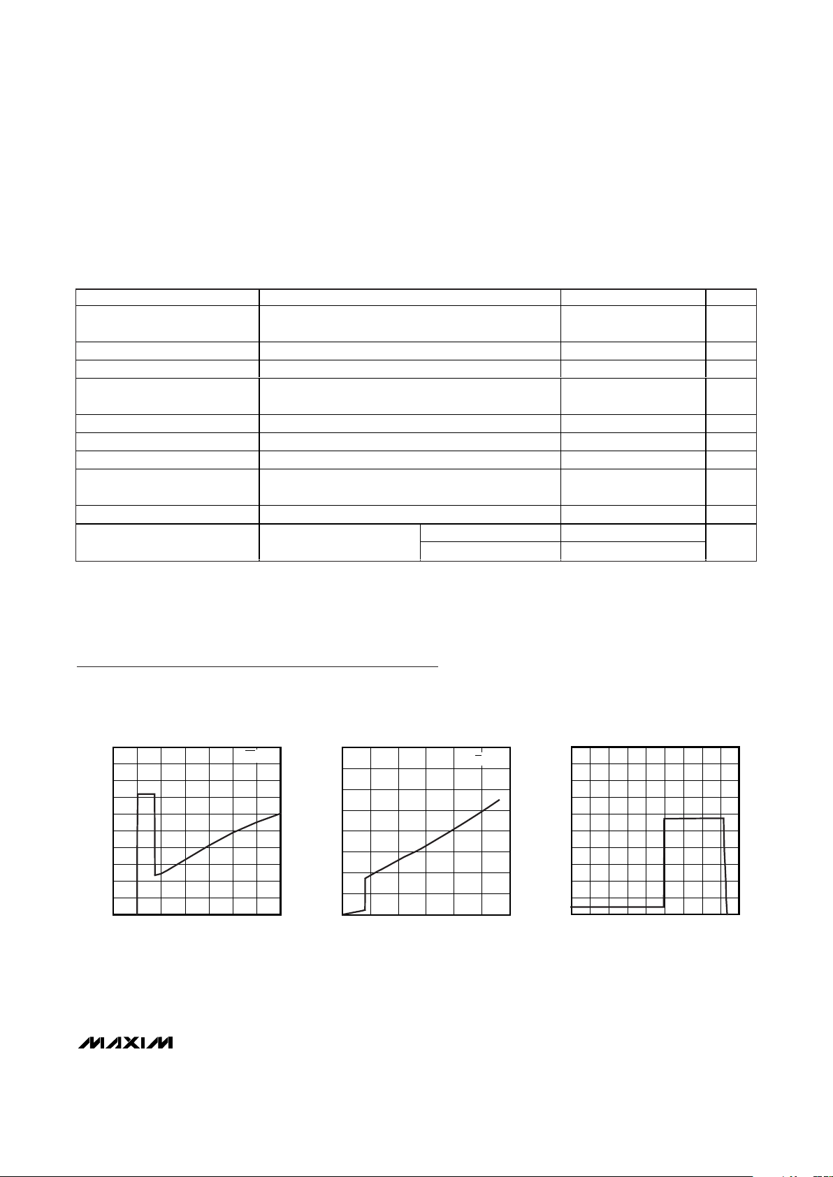
0
0.3
0.2
0.1
0.5
0.4
0.9
0.8
0.7
0.6
1.0
0 4 8 1216202428
SUPPLY CURRENT
vs. VOLTAGE
MAX8814 toc01
INPUT VOLTAGE (V)
SUPPLY CURRENT (mA)
EN = 0V
0
100
200
300
400
500
600
700
800
0105 15202530
DISABLED MODE SUPPLY CURRENT
vs. INPUT VOLTAGE
MAX8814 toc02
INPUT VOLTAGE (V)
SUPPLY CURRENT (μA)
VEN = 5V
0
200
100
400
300
600
500
700
900
800
1000
0 1.0 1.5 2.00.5 2.5 3.0 3.5 4.0 4.5
CHARGE CURRENT
vs. BATTERY VOLTAGE
MAX8814 toc03
BATTERY VOLTAGE (V)
CHARGE CURRENT (mA)
MAX8814
28V Linear Li+ Battery Charger with
Smart Autoboot Assistant
4 _______________________________________________________________________________________
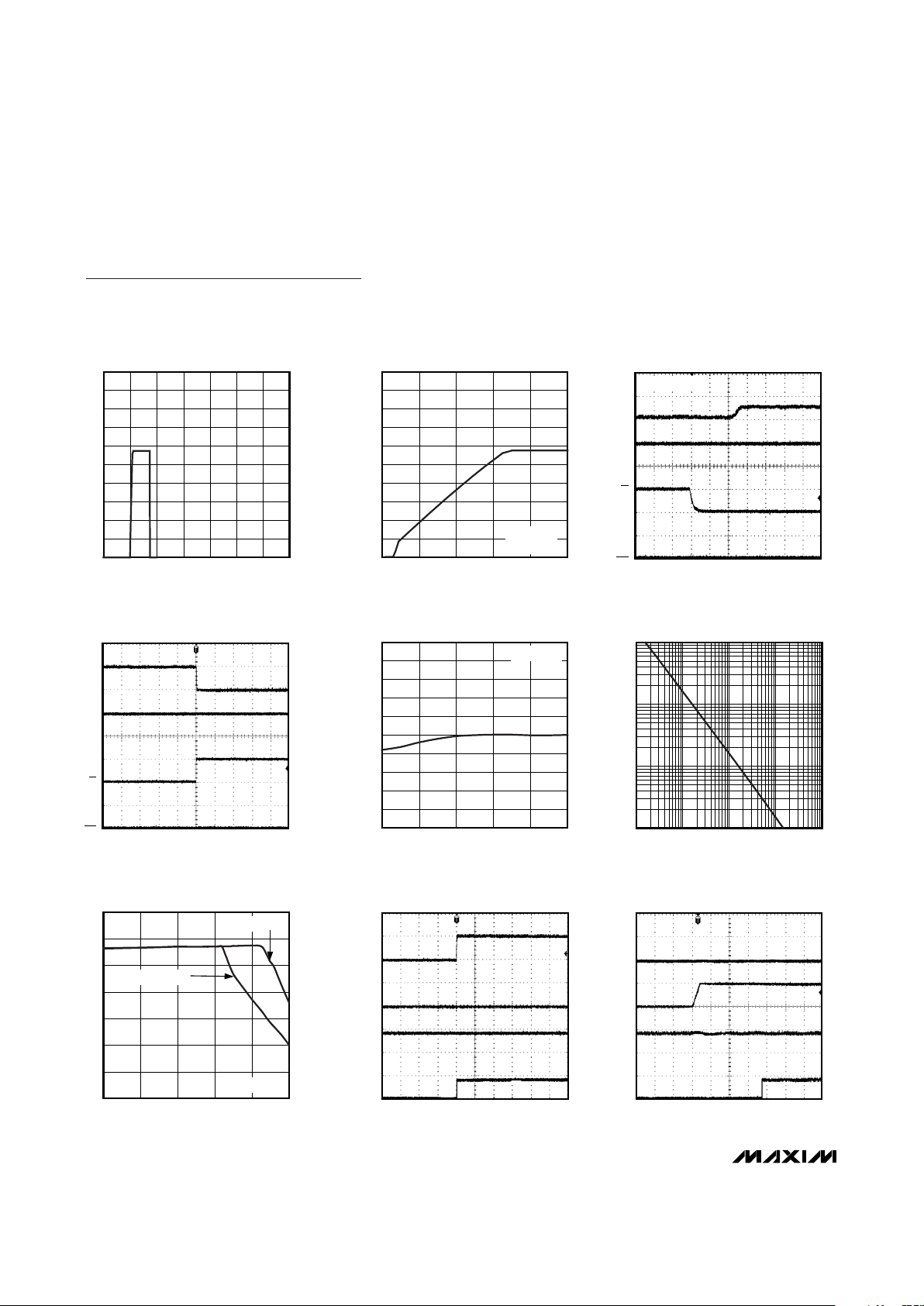
0
300
200
100
500
400
900
800
700
600
1000
0 4 8 12 16 20 24 28
CHARGE CURRENT
vs. INPUT VOLTAGE
MAX8814 toc04
INPUT VOLTAGE (V)
CHARGE CURRENT (mA)
0
300
200
100
400
500
600
700
800
900
1000
0 200100 300 400 500
CHARGE CURRENT vs. INPUT
VOLTAGE HEADROOM
MAX8814 toc05
VIN - V
BATT
(mV)
CHARGE CURRENT (mA)
V
BATT
= 4V
V
IN
RISING
40
μs/div
STARTUP INTO PRECHARGE
100mA/div
MAX8814 toc06
0A
5V/div
5V/div
5V/div
0V
0V
0V
I
BATT
V
IN
V
EN
V
POK
V
BATT
= 2V
100μs/div
SHUTDOWN
(FAST-CHARGE TO SHUTDOWN)
500mA/div
MAX8814 toc07
0A
0V
5V/div
5V/div
5V/div
0V
0V
I
BATT
V
IN
V
EN
V
POK
-1.0
-0.4
-0.6
-0.8
-0.2
0
0.2
0.4
0.6
0.8
1.0
-40 10-15 35 60 85
BATTERY REGULATION VOLTAGE
ACCURACY vs. AMBIENT TEMPERATURE
MAX8814 toc08
TEMPERATURE (°C)
BATTERY REGULATION VOLTAGE ACCURACY (%)
I
BATT
= 0A
CHARGE CURRENT vs. R
ISET
MAX8814 toc09
R
ISET
(kΩ)
CHARGE CURRENT (mA)
100010010
10
100
1000
1
1 10,000
0
200
100
400
300
600
500
700
-40 10-15 356085
CHARGE CURRENT vs. AMBIENT
TEMPERATURE
MAX8814 toc10
TEMPERATURE (°C)
CHARGE CURRENT (mA)
R
ISET
= 2.8kΩ
V
BATT
= 4V
V
BATT
= 3.2V
4μs/div
AUTOBOOT ENABLED
BY ABI SIGNAL
MAX8814 toc11
0V
0V
5V/div
5V/div
5V/div
5V/div
0V
0V
V
ABI
V
IN
V
BATT
V
ABO
4μs/div
AUTOBOOT ENABLED
BY INPUT SUPPLY
MAX8814 toc12
0V
5V/div
0V
5V/div
5V/div
5V/div
0V
0V
V
ABI
V
IN
V
BATT
V
ABO
Typical Operating Characteristics (continued)
(VIN= 5V, V
BATT
= 4V, R
POK
= 1MΩ to BATT, EN = 0V, R
ISET
= 2.8kΩ to GND, C
BATT
= 2.2µF, TA= -40°C to +85°C, unless other-
wise noted. Typical values are at T
A
= +25°C.)

MAX8814
28V Linear Li+ Battery Charger with
Smart Autoboot Assistant
_______________________________________________________________________________________ 5
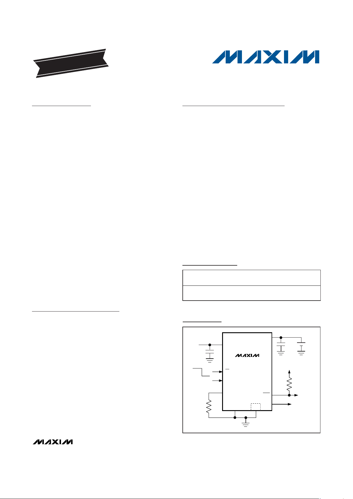
Pin Description
PIN NAME FUNCTION
1IN
Input Supply Voltage. Bypass IN to GND with a 1µF or larger ceramic capacitor to minimize line noise
and maximize input transient rejection.
2 GND
Ground. Connect GND and the exposed paddle to a large copper ground plane for maximum power
dissipation. Connect GND to the exposed paddle directly under the IC.
3 ISET
Charge-Current Program and Fast-Charge Current Monitor. Output current from ISET is 877.2µA per
ampere of battery charging current. Set the charging current by connecting a resistor (R2 in Figure 3)
from ISET to GND. I
FAST-CHARGE
= 1596V / R
ISET
. To configure the MAX8814 as a USB charger, see
Figure 4.
4 ABI
Autobooting External Input. See the Autobooting Assistant section and Table 1 for autobooting
conditions. ABI is pulled to GND through an internal 200kΩ resistor.
5 ABO
Autobooting Logic Output. See the Autobooting Assistant section and Table 1 for autobooting
conditions.
6 EN
Logic-Level Enable Input. Drive EN high to disable charger. Drive EN low or leave unconnected for
normal operation. EN has an internal 200kΩ pulldown resistor.
7 POK
Input-Voltage Status Indicator. Connect a 1MΩ pullup resistor from POK to an external system supply.
POK is an open-drain output that asserts low when VIN > 4.25V and (VIN - V
BATT
) ≥ 40mV. If V
BATT
≥
(V
IN
- 40mV), the IC is shut down and POK becomes high impedance.
8 BATT Battery Connection. Bypass BATT to GND with a minimum of 2.2µF of capacitor.
—EP
Exposed Paddle. Connect the exposed paddle to a large ground plane for maximum power
dissipation. Connect GND to the exposed paddle directly under the IC.

MAX8814
28V Linear Li+ Battery Charger with
Smart Autoboot Assistant
6 _______________________________________________________________________________________
Detailed Description
The MAX8814 charger uses voltage, current, and thermal-control loops to charge a single Li+ cell and protect the battery (Figure 1). When a Li+ battery with a
cell voltage below 2.5V is inserted, the MAX8814
charger enters the prequalification stage where it
precharges that cell with 10% of the user-programmed
fast-charge current (Figure 2). When the battery voltage
exceeds 2.5V, the charger soft-starts as it enters the
fast-charge stage. In the MAX8814, the fast-charge
current level is programmed through a resistor from
ISET to GND. As the battery voltage approaches 4.2V,
the charging current is reduced. Once the battery voltage reaches 4.2V, the IC then enters a constant voltage
regulation mode to maintain the battery at full charge.
Thermal Regulation
The thermal-regulation loop limits the MAX8814 die
temperature to +115°C by reducing the charge current
as necessary. This feature not only protects the IC from
overheating, but also allows a higher charge current
without risking damage to the IC.
6 _______________________________________________________________________________________
OUTPUT DRIVER,
CURRENT SENSE,
AND LOGIC
TEMPERATURE
SENSOR
VL
REGULATOR
REF
REFOK
V
IN
OVLO
VL
UVLO
V
REF
V
REF
LOGIC
BATT
ISET
ABI
ABO
EN
POK
IN
BATT
IN
BATT
POK
200kΩ
GND
EP
+115°C
Li+
C3
2.2μF
V
I/O
200kΩ
C1
1μF
R2
2.8kΩ
4.25V TO 28V
R3
1MΩ
MAX8814
V
L
V
REF
Figure 1. Functional Diagram

MAX8814
28V Linear Li+ Battery Charger with
Smart Autoboot Assistant
_______________________________________________________________________________________ 7
Charger Enable Input
The MAX8814 contains an active-low logic input (EN)
used to enable the charger. Drive EN low, leave unconnected, or connect to GND to enable the chargercontrol circuitry. Drive EN high to disable the chargercontrol circuitry. EN has an internal 200kΩ pull-down
resistor.
POK
Output
The open-drain POK output asserts low when VIN≥
4.25V and (VIN- V
BATT
) ≥ 40mV (typ, VINrising). POK
requires an external pullup resistor (1MΩ typ) to an
external power supply. POK is high impedance when
V
BATT
≥ (VIN- 40mV).
Autobooting Assistant
The MAX8814 contains an autobooting assistant circuit
that generates an enable signal for system booting
(ABO). The booting assistant functions as an internal
“OR” gate (Figure 1). The first input is dependent on
the input voltage (VIN), and the second input is an
external signal applied to ABI. The first input (POK) is
driven high once VIN≥ 4.25V and (VIN- V
BATT
) ≥ 40mV
(typ, VINrising).
The second input signal (ABI) is driven by an external
source. ABI enables an autoboot signal (ABO high)
when a battery is connected at BATT and is independent
of POK. If POK is pulled low, the booting assistant
always drives ABO high, regardless of ABI (see Table 1).
ABI is pulled to GND through an internal 200kΩ resistor.
If ABI is driven externally, a RC filter (R1 and C2 of
Figure 3) is required for ESD protection and noise filtering. If ABI is supplied by a system’s internal GPIO, or
logic, the RC filter is not required.
Soft-Start
The soft-start algorithm activates when entering fastcharge mode. In the MAX8814, when the prequalification state is complete (V
BATT
≥ 2.5V), the charging
current ramps up in 250µs to the full charging current.
This reduces the inrush current on the input supply.
_______________________________________________________________________________________ 7
V
BATT
< 2.5V
PRECHARGE
10% CHARGE CURRENT
FAST-CHARGE
CONSTANT-CURRENT CHARGE
100% CHARGE CURRENT
VOLTAGE REGULATION
CONSTANT VOLTAGE CHARGE
REGULATED 4.2V AT BATT
(V
IN
- V
BATT
) < 30mV
V
BATT
< 2.4V
V
BATT
≥ 2.5V
VIN < 7V, AND
(V
IN
- V
BATT
) ≥ 40mV, AND
IC ENABLED
SHUTDOWN
CHARGER = DISABLED
V
IN
> 7V, OR
(V
IN
- V
BATT
) < 30mV, OR
IC DISABLED
ASYNCHRONOUS
FROM ANYWHERE
V
IN
> 7V, OR
(V
IN
- V
BATT
) < 30mV, OR
IC DISABLED
V
BATT
≥ 4.2V
V
BATT
< 4.2V
Figure 2. Charge-State Diagram
ABI BATT POK CHARGER STATE ABO
Low Present Hi-Z Shutdown Low
High Present Hi-Z Shutdown High
X Not present Low
Fast-charge/voltage
regulation
High
X Present Low
Fast-charge/voltage
regulation
High
Table 1. ABO and POK States
X = Don’t care.

MAX8814
Applications Information
Charge-Current Selection
The maximum charging current is programmed by an
external resistor connected from ISET to GND (R
ISET
).
Calculate R
ISET
as follows:
where I
FAST-CHARGE
is in amperes and R
ISET
is in
ohms. ISET can be used to monitor the fast-charge current level. The output current from ISET is 877.2µA per
ampere of charging current. The output voltage at ISET
is proportional to the charging current:
The voltage at ISET is nominally 1.4V at the selected
fast-charge current and falls with charging current as
the cell becomes fully charged or as the thermal-regulation circuitry activates.
Capacitor Selection
Connect a ceramic capacitor from BATT to GND for
proper stability. Use a 2.2µF X5R ceramic capacitor for
most applications. Connect a 1µF ceramic capacitor
from IN to GND. Use a larger input bypass capacitor
for high charging currents to reduce supply noise.
Thermal Considerations
The MAX8814 is available in a thermally enhanced
TDFN package with an exposed paddle. Connect the
exposed paddle to a large copper ground plane to provide a thermal contact between the device and the circuit board for increased power dissipation. The exposed
paddle transfers heat away from the device, allowing the
IC to charge the battery with maximum current, while
minimizing the increase in die temperature.
DC Input Sources
The MAX8814 operates from a well-regulated DC
source. The full charging input voltage range is 4.25V
to 7V. The device can withstand up to 28V on the input
without damage to the IC. If VINis greater than 7V, the
internal overvoltage-protection circuitry disables charging until the input falls below 7V. An appropriate power
supply must provide at least 4.25V at the desired peak
charging current.
V
IR
ISET
CHARGE ISET
=
×
1140
R
V
I
ISET
FAST CHARGE
=
−
1596
28V Linear Li+ Battery Charger with
Smart Autoboot Assistant
8 _______________________________________________________________________________________
IN
ABI
ISET
ABO
BATT
GND
EP
VI/O
EN
GPIO
GPIO
ADC
POWER
SUPPLY
ON
SYSTEM
POK
GND
FACTORY TEST
FIXTURE
OR
AC ADAPTER
C3
2.2μF
Li+
R3
1MΩ
R4
10kΩ
C4
0.1μF
R2
2.8kΩ
C1
1μF
R1
10kΩ
C2
0.1μF
MAX8814
Figure 3. Microprocessor-Interfaced Li+ Battery Charger

Application Circuits
Microprocessor-Interfaced Charger
Figure 3 shows the MAX8814 as a microprocessorcooperated Li+ battery charger. The MAX8814 begins
charging the battery when EN is low. The microprocessor can drive EN high to disable the charger. The
MAX8814 generates a POK signal to indicate the presence of an input supply. By monitoring V
ISET
, the system can measure the charging current and decide
when to terminate the charge.
USB-Powered Li-Ion Charger
The universal serial bus (USB) provides a high-speed
serial communication port as well as power for the
remote device. The MAX8814 can be configured to
charge a battery at the highest current possible from
the host port. Figure 4 shows the MAX8814 as a USB
battery charger. To make the circuit compatible with
either 100mA or 500mA USB ports, the circuit initializes
at 100mA charging current. The microprocessor then
enumerates the host to determine its current capability.
If the host port is capable, the charging current is
increased to 425mA to avoid exceeding the 500mA
USB specification.
Layout and Bypassing
Place the input and output capacitors as close as possible to the IC. Provide a large copper ground plane to
allow the exposed paddle to sink heat away from the
IC. Connect the battery to BATT as close as possible to
the IC to provide accurate battery voltage sensing.
Make all high-current traces short and wide to minimize
voltage drops. A sample layout is available in the
MAX8814 Evaluation Kit to speed designs.
Chip Information
PROCESS: BiCMOS
MAX8814
28V Linear Li+ Battery Charger with
Smart Autoboot Assistant
_______________________________________________________________________________________ 9
IN
ABI
ISET
ABO
BATT
GND
EP
V
I/O
EN
GPIO
GPIO
GPIO
ADC
POWER
SUPPLY
ON
SYSTEM
POK
GND
USB PORT
C3
2.2μF
Li+
R3
1MΩ
R4
10kΩ
C4
0.1μF
R2
15.8kΩ
C1
1μF
MAX8814
VBUS
+
R5
4.99kΩ
N
Figure 4. USB Battery Charger

MAX8814
28V Linear Li+ Battery Charger with
Smart Autoboot Assistant
10 ______________________________________________________________________________________
134
865
BATT EN ABO
MAX8814
2
7
POK
IN ISET ABIGND
TDFN
2mm x 2mm
TOP VIEW
+
EXPOSED PADDLE
Pin Configuration

MAX8814
28V Linear Li+ Battery Charger with
Smart Autoboot Assistant
______________________________________________________________________________________ 11
Package Information
(The package drawing(s) in this data sheet may not reflect the most current specifications. For the latest package outline information
go to www.maxim-ic.com/packages
.)
PACKAGE OUTLINE
21-0168
2
1
D
6 & 8L TDFN EXPOSED PAD, 2x2x0.80mm
8L TDFN EXPOSED PADS.EPS

MAX8814
28V Linear Li+ Battery Charger with
Smart Autoboot Assistant
Maxim cannot assume responsibility for use of any circuitry other than circuitry entirely embodied in a Maxim product. No circuit patent licenses are
implied. Maxim reserves the right to change the circuitry and specifications without notice at any time.
12
____________________Maxim Integrated Products, 120 San Gabriel Drive, Sunnyvale, CA 94086 408-737-7600
© 2007 Maxim Integrated Products is a registered trademark of Maxim Integrated Products, Inc.
SYMBOL
COMMON DIMENSIONS
2.101.90
0.80
MAX.
0.70
MIN.
0.20 REF.
0.40
0.05
2.10
0.20
0.00
1.90
D
A
L
A1
E
A2
k
1.60±0.10 1.30 REF
[(N/2)-1] x e
0.30±0.05
b
0.65 TYP.
e
PACKAGE VARIATIONS
PKG. CODE
0.90±0.10
E2D2
6
N
T622-1
0.25 MIN.
PACKAGE OUTLINE
21-0168
2
2
D
6 & 8L TDFN EXPOSED PAD, 2x2x0.80mm
1.30±0.10 1.50 REF0.25±0.050.50 TYP. 0.70±0.108T822-1
0.150
r
0.125
1.20±0.10 1.50 REF0.25±0.050.50 TYP. 0.80±0.108T822-2 0.125
Package Information (continued)
(The package drawing(s) in this data sheet may not reflect the most current specifications. For the latest package outline information
go to www.maxim-ic.com/packages
.)
 Loading...