MAXIM MAX8804W, MAX8804Y, MAX8804Z Technical data
General Description
The MAX8804W/MAX8804Y/MAX8804Z intelligent,
dual-input, stand-alone, constant-current, constant-voltage (CCCV), thermally regulated linear chargers are
designed for a single-cell lithium-ion (Li+) battery. They
integrate the current-sense circuit, MOS pass element,
thermal-regulation circuitry, and overvoltage protection
(OVP), and eliminate the reverse-blocking Schottky
diode to create a simple and small charging solution for
handheld equipment.
The MAX8804W/MAX8804Z function as stand-alone
chargers to control the charging sequence from the prequalification state through fast-charge, top-off charge,
and full-charge indication. The MAX8804Y eliminates the
prequalification state to allow startup into a load without
a battery. Proprietary thermal-regulation circuitry limits
the die temperature when fast-charging or while
exposed to high ambient temperatures, allowing maximum charging current without damaging the IC.
The MAX8804Y/MAX8804Z achieve high flexibility by
providing an adjustable DC/USB fast-charge current
through a simple single-wire interface (SET input). The
chargers automatically select between either a USB or
AC adapter input source. The AC adapter charge current is programmable from 400mA to 700mA in 50mA
steps through a serial interface. The USB charge current is programmable to 95mA, 380mA, or 475mA
through the same interface. Other features include an
active-low battery charging-status indicator (CHG), an
active-low power-OK indicator (POK), an active-low
USB input detection output (USBPWR) on the
MAX8804Y/MAX8804Z, and battery pack detection
(DETBAT) on the MAX8804W.
The MAX8804W/MAX8804Y/MAX8804Z accept a 4.15V
to 30V DC source voltage or a 4.15V to 16V USB input
voltage, but disable charging when either input voltage
exceeds 7.5V to protect against unqualified or faulty
input sources. The MAX8804W/MAX8804Y/MAX8804Z
operate over the extended temperature range (-40°C to
+85°C) and are available in a tiny 8-pin thermally
enhanced 2mm x 3mm TDFN package.
Applications
Cell Phones/Smartphones
Digital Cameras
Portable Media Players
MP3 Players
Other Handheld Devices
Features
♦ Complete Chargers for Single-Cell Li+ Battery
♦ Dual-Input, 30V AC Adapter/16V USB
♦ No External FET, Blocking Diode, or Sense
Resistor Required
♦ Automatic USB/AC Adapter Input Selection
♦ Easy Programmable Fast-Charge Current and
Top-Off Threshold
♦ Proprietary Die Temperature Regulation Control
♦ ±5% Fast-Charge Current-Limit Accuracy
♦ Battery Pack Detection Input (MAX8804W)
♦ Power-Present and Charger-Status Outputs
♦ No Prequalification Charge (MAX8804Y)
♦ Tiny 2mm x 3mm Thermally Enhanced TDFN
Package
♦ USB Charging Protected by US Patent #6,507,172
MAX8804W/MAX8804Y/MAX8804Z
High-Voltage, Dual-Input, USB/AC
Adapter Chargers in 2mm x 3mm TDFN
________________________________________________________________
Maxim Integrated Products
1
19-0785; Rev 1; 10/07
For pricing, delivery, and ordering information, please contact Maxim Direct at 1-888-629-4642,
or visit Maxim's website at www.maxim-ic.com.
EVALUATION KIT
AVAILABLE
Ordering Information
*
EP = Exposed paddle.
+
Denotes a lead-free package.
Note: All devices are specified to operate over the -40°C to
+85°C operating temperature range.
Pin Configuration appears at end of data sheet.
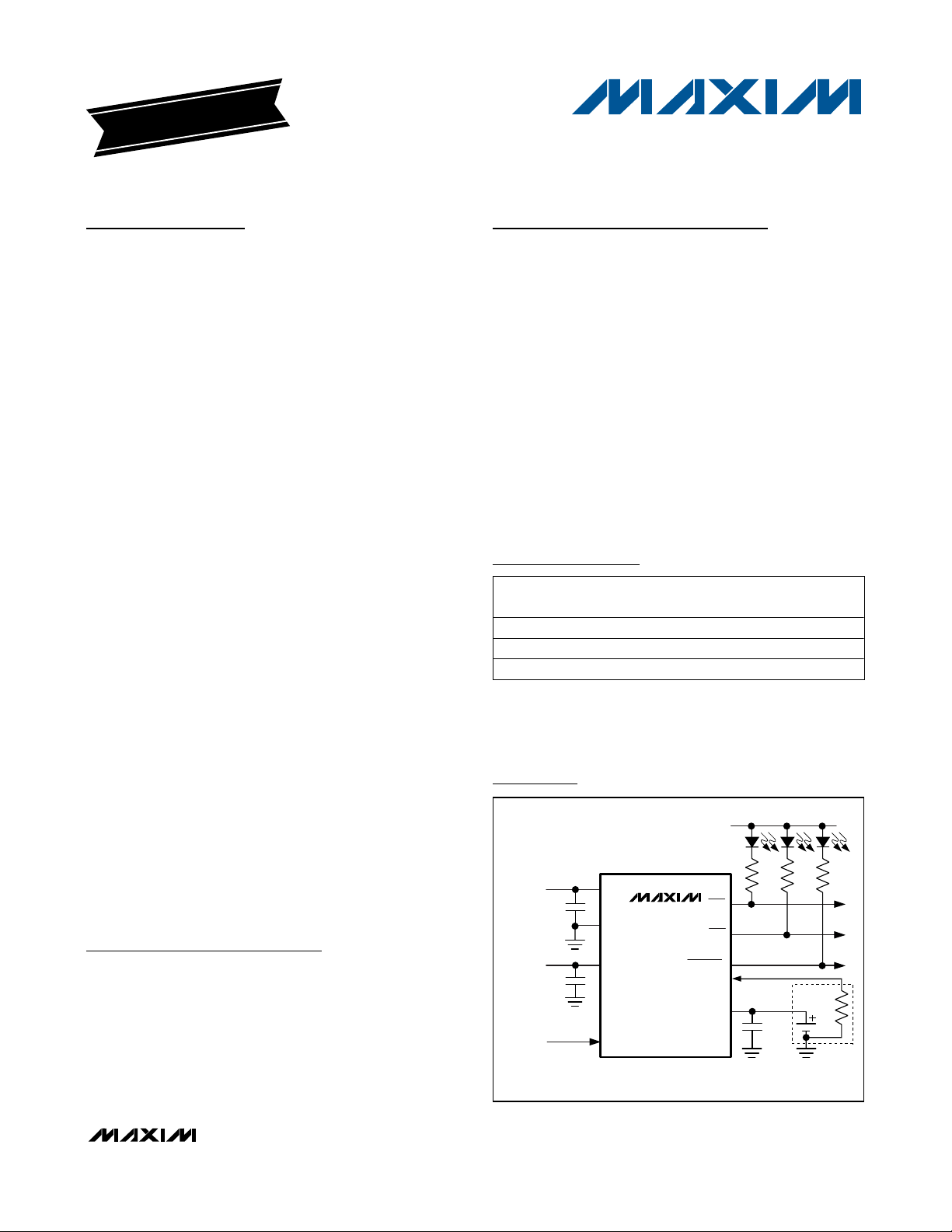
DC
GND
USB
SET
CHG
POK
<USBPWR>
BAT
+3.3V
AC
ADAPTER
USB
PORT
ENABLE/DISABLE
AND PROGRAMMING
Li+
1μF
2.2μF
MAX8804W
MAX8804Y
MAX8804Z
1μF
(DETBAT)
NOTE: () FOR MAX8804W, <> FOR MAX8804Y/MAX8804Z
Typical Application Circuit
PART
MAX8804WETA+ 8 TDFN-EP* T823+1 AAP
MAX8804YETA+ 8 TDFN-EP* T823+1 AAD
MAX8804ZETA+ 8 TDFN-EP* T823+1 AAC
PINPACKAGE
PKG
CODE
TOP
MARK
MAX8804W/MAX8804Y/MAX8804Z
High-Voltage, Dual-Input, USB/AC
Adapter Chargers in 2mm x 3mm TDFN
2 _______________________________________________________________________________________
ABSOLUTE MAXIMUM RATINGS
ELECTRICAL CHARACTERISTICS
((VDC= 5V, V
SET
= 0V) or (V
USB
= 5V, V
SET
= 5V), V
BAT
= unconnected, V
DETBAT
= 0V (MAX8804W), TA= -40°C to +85°C, unless
otherwise noted.) (Note 1)
Stresses beyond those listed under “Absolute Maximum Ratings” may cause permanent damage to the device. These are stress ratings only, and functional
operation of the device at these or any other conditions beyond those indicated in the operational sections of the specifications is not implied. Exposure to
absolute maximum rating conditions for extended periods may affect device reliability.
DC to GND .............................................................-0.3V to +30V
USB to GND ...........................................................-0.3V to +16V
BAT, CHG, SET, POK, USBPWR, DETBAT
to GND...............................................................-0.3V to +5.5V
Continuous Power Dissipation (T
A
= +70°C)
8-Pin TDFN 2mm x 3mm (derate 16.7mW/°C above +70°C)
(multilayer board) .......................................................1333mW
Operating Temperature Range ...........................-40°C to +85°C
Junction Temperature......................................................+150°C
Storage Temperature Range .............................-65°C to +150°C
Lead Temperature (soldering, 10s) .................................+300°C
DC AND USB
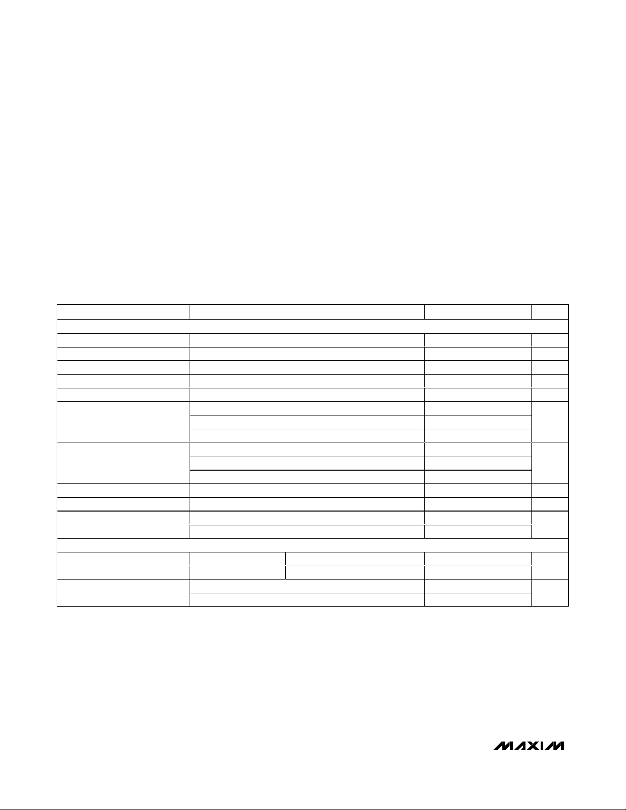
DC Input Voltage Range 028V
USB Input Voltage Range 014V
Input Operating Range (Notes 2, 3) 4.15 7.00 V
Input Undervoltage Threshold VIN rising, 500mV hysteresis (typ) (Note 2) 3.85 4.0 4.15 V
Input Overvoltage Threshold VIN rising, 200mV hysteresis (typ) (Note 2) 7.2 7.5 7.8 V
USB Input Supply Current
DC to BAT On-Resistance VDC = 3.7V, V
USB to BAT On-Resistance V
Input to BAT Comparator
Threshold (Note 2)
BAT
BAT Regulation Voltage I
Battery Removal Detection
Threshold
PARAMETER CONDITIONS MIN TYP MAX UNITS
V
V
V
VDC = 0V, V
V
V
VIN rising 145 260 385
V
BAT
V
Hysteresis 0.1
= 0V, I
USB
SET
= V
DC
SET
USB
USB
falling 55
IN
= 0mA
BAT
BAT
= 5V, standby mode 300 550DC Input Supply Current
= 4.3V, shutdown mode 300 550
BAT
SET
= 0V, standby mode 300 550
= V
= 4.3V, shutdown mode 300 550
BAT
= 3.7V, V
rising 4.40 4.67 4.90
= 0mA, charge mode 800 1200
= 5V, I
BAT
= 3.6V 0.55 1.0 Ω
BAT
= 3.6V 0.65 1.2 Ω
BAT
TA = +25°C 4.179 4.200 4.221
T
= 0mA, charge mode 800 1200
= -40°C to +85°C 4.158 4.200 4.242
A
µA
µA
mV
V
V
MAX8804W/MAX8804Y/MAX8804Z
High-Voltage, Dual-Input, USB/AC
Adapter Chargers in 2mm x 3mm TDFN
_______________________________________________________________________________________ 3
ELECTRICAL CHARACTERISTICS (continued)
((VDC= 5V, V
SET
= 0V) or (V
USB
= 5V, V
SET
= 5V), V
BAT
= unconnected, V
DETBAT
= 0V (MAX8804W), TA= -40°C to +85°C, unless
otherwise noted.) (Note 1)
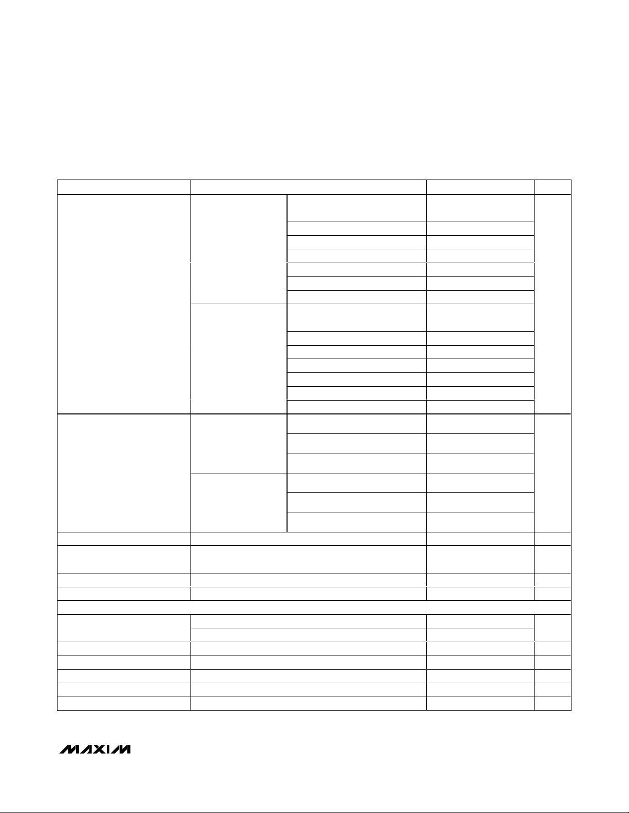
DC Charging Current
USB Charging Current
Soft-Start Time Ramping time from 0 to 500mA 250 µs
BAT Prequal Threshold
BAT Prequal Charge Current MAX8804W/MAX8804Z only 95 mA
BAT Leakage Current VDC = V
SET
Logic Input Thresholds
Logic-High Time Pulse width required to program DC charge current 1 1000 µs
Logic-Low Time Pulse width required to program USB charge current 1 1000 µs
SET DC Mode Shutdown Delay V
SET USB Mode Shutdown Delay VDC = 0V, V
SET Internal Pulldown Resistor 24MΩ
PARAMETER CONDITIONS MIN TYP MAX UNITS
V
V
rising edge detection
on SET
(MAX8804Y/
MAX8804Z)
V
V
edge detection on SET
(MAX8804W)
V
V
edge detection on SET
(MAX8804Y/
MAX8804Z)
V
V
edge detection on SET
(MAX8804W)
MAX8804W/MAX8804Z only, V
hysteresis (typ)
V
V
= 0V,
USB
= 3.6V,
BAT
= 0V,
USB
= 3.6V, rising
BAT
= 0V,
DC
= 3.6V, rising
BAT
= 0V,
DC
= 3.6V, rising
BAT
= 0V, V
USB
rising 1.6
SET
falling 0.4
SET
= 0V, VDC = 5V, measured from V
USB
USB
Default and 1st to 3rd interface
pulse
4th to 7th interface pulse 523 550 578
8th to 11th interface pulse 570 600 630
12th to 15th interface pulse 428 450 473
16th to 19th interface pulse 380 400 420
20th to 23rd interface pulse 618 650 683
24th to 27th interface pulse 665 700 735
Default and 1st to 3rd interface
pulse
4th to 7th interface pulse 523 550 578
8th to 11th interface pulse 475 500 525
12th to 15th interface pulse 380 400 420
16th to 19th interface pulse 570 600 630
20th to 23th interface pulse 618 650 683
24th to 27th interface pulse 665 700 735
Default 90 95 100
1st interface pulse 360 380 400
2nd interface pulse 450 475 500
Default 360 380 400
1st interface pulse 450 475 500
2nd interface pulse 90 95 100
rising, 300mV
BAT
= 4.2V 2 µA
BAT
SET
= 5V, measured from V
SET
475 500 525
428 450 473
2.35 2.50 2.65 V
low to high 1.5 2 2.5 ms
high to low 1.5 2 2.5 ms
mA
mA
V
MAX8804W/MAX8804Y/MAX8804Z
High-Voltage, Dual-Input, USB/AC
Adapter Chargers in 2mm x 3mm TDFN
4 _______________________________________________________________________________________
ELECTRICAL CHARACTERISTICS (continued)
((VDC= 5V, V
SET
= 0V) or (V
USB
= 5V, V
SET
= 5V), V
BAT
= unconnected, V
DETBAT
= 0V (MAX8804W), TA= -40°C to +85°C, unless
otherwise noted.) (Note 1)
Note 1: Devices are 100% production tested at TA= +25°C. Limits over the operating temperature range are guaranteed by design
and characterization.
Note 2: V
IN
refers to the input for the IC. For the MAX8804W/MAX8804Y/MAX8804Z, VINis VDCwith V
USB
= 0V or V
USB
with VDC=
0V.
Note 3: Guaranteed by undervoltage and overvoltage threshold testing. For charge completion, the input voltage must be greater
than 4.28V.
Note 4: This hysteresis is for all charge current except 95mA. In the case of 95mA charge current, voltage-mode to current-mode
detection gives indication of charge mode.
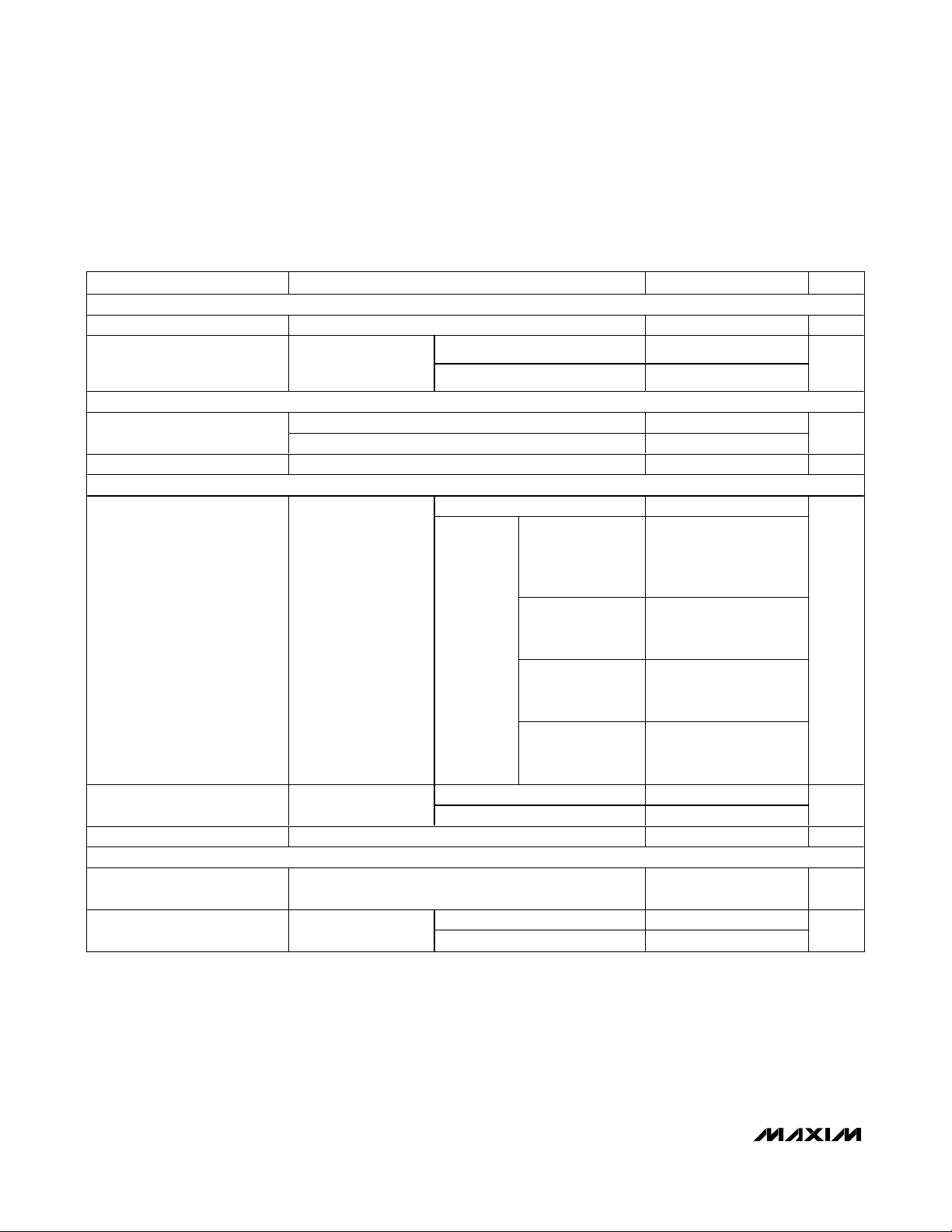
POK, CHG, USBPWR (USBPWR only for MAX8804Y/MAX8804Z)
Logic Output-Voltage Low I
Logic Output-Current High
DETBAT (MAX8804W only)
Logic Input Theshold
Pullup Resistor 63 kΩ
CHG
PARAMETER CONDITIONS MIN TYP MAX UNITS
= I
POK
V
POK
V
USBPWR
V
= V
DC
= V
= I
CHG
CHG
= 5.5V,
= 0V
USB
=
= 5mA 60 500 mV
USBPWR
TA = +25°C 0.001 1
T
= +85°C 0.01
A
Rising 1.6
Falling 0.4
VDC = 0V, V
= 5V 60 80 100
USB
Default, 4th, 8th,
12th, 16th, 20th,
24th, 28th interface
60 80 100
pulse
µA
V
1st, 5th, 9th, 13th,
17th, 21st, 25th
interface pulse
67.5 90 112.5
CHG Top-Off Threshold
I
falling, battery is
BAT
charged, rising edge
on SET
V
V
DC
USB
= 5V,
= 0V
2nd, 6th, 10th,
14th, 18th, 22nd,
75 100 125
26th interface pulse
3rd, 7th, 11th, 15th,
19th, 23rd, 27th
CHG Hysteresis
CHG Detection Delay I
I
rising after top-off
BAT
is detected (Note 4)
falls below top-off threshold 3 4 5 ms
BAT
DC mode 57
USB mode 51
interface pulse
52.7 70 87.5
THERMAL LOOP
Thermal-Regulation Set Point
Thermal-Regulation Gain
Junction temperature when the charge current is reduced,
T
rising
J
DC charging -40
J
BAT
for
USB charging -24
Reduction of I
increase of T
+105 °C
mA
mA
mA/°C
MAX8804W/MAX8804Y/MAX8804Z
High-Voltage, Dual-Input, USB/AC
Adapter Chargers in 2mm x 3mm TDFN
_______________________________________________________________________________________ 5
Typical Operating Characteristics
(V
BAT
= 3.6V; DC charge mode: VDC= 5V, V
USB
= 0V, V
DETBAT
= 0V (only for MAX8804W), V
SET
= 0V or unconnected; USB charge
mode: V
USB
= 5V, VDC= 0V, V
SET
= 5V; TA= +25°C, unless otherwise noted.)
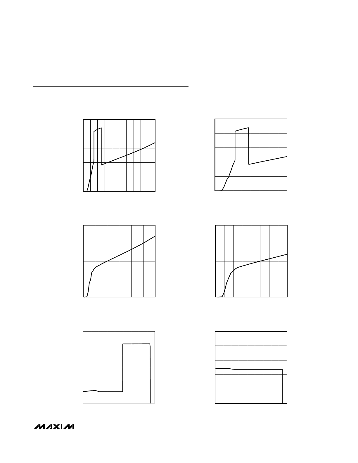
STANDBY-MODE SUPPLY CURRENT
vs. INPUT VOLTAGE (USB CHARGING MODE)
INPUT VOLTAGE (V)
SUPPLY CURRENT (mA)
MAX8804Y/Z toc04
0246810121416
0
0.2
0.4
0.6
0.8
CHARGE CURRENT vs. BATTERY VOLTAGE
(DC CHARGING MODE)
BATTERY VOLTAGE (V)
CHARGE CURRENT (mA)
MAX8804Y/Z toc05
0 0.5 1.0 1.5 2.0 2.5 3.0 3.5 4.0 4.5
0
100
200
300
400
500
600
CHARGE CURRENT vs. BATTERY VOLTAGE
(USB CHARGING MODE)
BATTERY VOLTAGE (V)
CHARGE CURRENT (mA)
MAX8804Y/Z toc06
0 0.5 1.0 1.5 2.0 2.5 3.0 3.5 4.0 4.5
0
40
80
120
160
200
SUPPLY CURRENT vs. INPUT VOLTAGE
1.0
0.8
0.6
0.4
SUPPLY CURRENT (mA)
0.2
0
036912151821242730
DISABLED-MODE SUPPLY CURRENT
vs. INPUT VOLTAGE (DC CHARGING MODE)
0.8
0.6
(DC CHARGING MODE)
MAX8804Y/Z toc01
INPUT VOLTAGE (V)
MAX8804Y/Z toc03
SUPPLY CURRENT vs. INPUT VOLTAGE
1.0
0.8
0.6
0.4
SUPPLY CURRENT (mA)
0.2
0
(USB CHARGING MODE)
MAX8804Y/Z toc02
0246810121416
INPUT VOLTAGE (V)
SUPPLY CURRENT (mA)
0.4
0.2
0
0 5 10 15 20 25 30
INPUT VOLTAGE (V)
CHARGE CURRENT
vs. AMBIENT TEMPERATURE
AMBIENT TEMPERATURE (°C)
CHARGE CURRENT (mA)
MAX8804Y/Z toc13
-40 -15 10 35 60 85
200
300
400
500
600
700
DC CHARGE MODE 650mA
BATTERY REGULATION VOLTAGE
vs. LOAD CURRENT
LOAD CURRENT (mA)
BATTERY REGULATION VOLTAGE (V)
MAX8804Y/Z toc14
0 100 200 300 400 500 600 700
4.10
4.15
4.20
4.25
4.30
550mA CHARGE-CURRENT SETTING
BATTERY REGULATION VOLTAGE
vs. AMBIENT TEMPERATURE
AMBIENT TEMPERATURE (°C)
BATTERY REGULATION VOLTAGE (V)
MAX8804Y/Z toc12
-40 -15 10 35 60 85
4.180
4.186
4.192
4.198
4.204
4.210
USB MODE
DC MODE
MAX8804W/MAX8804Y/MAX8804Z
High-Voltage, Dual-Input, USB/AC
Adapter Chargers in 2mm x 3mm TDFN
6 _______________________________________________________________________________________
Typical Operating Characteristics (continued)
(V
BAT
= 3.6V; DC charge mode: VDC= 5V, V
USB
= 0V, V
DETBAT
= 0V (only for MAX8804W), V
SET
= 0V or unconnected; USB charge
mode: V
USB
= 5V, VDC= 0V, V
SET
= 5V; TA= +25°C, unless otherwise noted.)
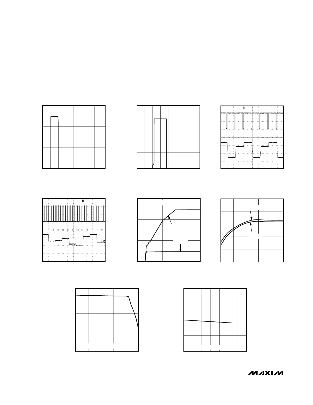
CHARGE CURRENT
vs. DC INPUT VOLTAGE
600
120
CHARGE CURRENT
vs. USB INPUT VOLTAGE
CHARGE CURRENT vs. SET PULSE
(USB CHARGING MODE) (MAX8804Y/MAX8804Z)
MAX8804Y/Z toc09
500
400
300
200
CHARGE CURRENT (mA)
100
0
0 5 10 15 20 25 30
INPUT VOLTAGE (V)
CHARGE CURRENT vs. SET PULSE
(DC CHARGING MODE) (MAX8804Y/MAX8804Z)
V
SET
700mA
I
CHG
500mA
550mA
600mA
450mA
650mA
400mA
MAX8804Y/Z toc10
700mA
2ms/div
500mA
MAX8804Y/Z toc07
1V/div
200mA/div
90
60
CHARGE CURRENT (mA)
30
0
0246810121416
INPUT VOLTAGE (V)
CHARGE CURRENT
vs. INPUT VOLTAGE HEADROOM
600
INPUT VOLTAGE DECREASING
500
400
300
200
CHARGE CURRENT (mA)
100
0
0 100 200 300 400 500
INPUT VOLTAGE HEADROOM (mV)
DC MODE
USB MODE
V
MAX8804Y/Z toc08
I
CHG
MAX8804Y/Z toc11
SET
475mA
475mA
380mA 380mA
95mA 95mA
2ms/div
1V/div
475mA
200mA/div
95mA
 Loading...