

General Description
The MAX8804W/MAX8804Y/MAX8804Z intelligent,
dual-input, stand-alone, constant-current, constant-voltage (CCCV), thermally regulated linear chargers are
designed for a single-cell lithium-ion (Li+) battery. They
integrate the current-sense circuit, MOS pass element,
thermal-regulation circuitry, and overvoltage protection
(OVP), and eliminate the reverse-blocking Schottky
diode to create a simple and small charging solution for
handheld equipment.
The MAX8804W/MAX8804Z function as stand-alone
chargers to control the charging sequence from the prequalification state through fast-charge, top-off charge,
and full-charge indication. The MAX8804Y eliminates the
prequalification state to allow startup into a load without
a battery. Proprietary thermal-regulation circuitry limits
the die temperature when fast-charging or while
exposed to high ambient temperatures, allowing maximum charging current without damaging the IC.
The MAX8804Y/MAX8804Z achieve high flexibility by
providing an adjustable DC/USB fast-charge current
through a simple single-wire interface (SET input). The
chargers automatically select between either a USB or
AC adapter input source. The AC adapter charge current is programmable from 400mA to 700mA in 50mA
steps through a serial interface. The USB charge current is programmable to 95mA, 380mA, or 475mA
through the same interface. Other features include an
active-low battery charging-status indicator (CHG), an
active-low power-OK indicator (POK), an active-low
USB input detection output (USBPWR) on the
MAX8804Y/MAX8804Z, and battery pack detection
(DETBAT) on the MAX8804W.
The MAX8804W/MAX8804Y/MAX8804Z accept a 4.15V
to 30V DC source voltage or a 4.15V to 16V USB input
voltage, but disable charging when either input voltage
exceeds 7.5V to protect against unqualified or faulty
input sources. The MAX8804W/MAX8804Y/MAX8804Z
operate over the extended temperature range (-40°C to
+85°C) and are available in a tiny 8-pin thermally
enhanced 2mm x 3mm TDFN package.
Applications
Cell Phones/Smartphones
Digital Cameras
Portable Media Players
MP3 Players
Other Handheld Devices
Features
♦ Complete Chargers for Single-Cell Li+ Battery
♦ Dual-Input, 30V AC Adapter/16V USB
♦ No External FET, Blocking Diode, or Sense
Resistor Required
♦ Automatic USB/AC Adapter Input Selection
♦ Easy Programmable Fast-Charge Current and
Top-Off Threshold
♦ Proprietary Die Temperature Regulation Control
♦ ±5% Fast-Charge Current-Limit Accuracy
♦ Battery Pack Detection Input (MAX8804W)
♦ Power-Present and Charger-Status Outputs
♦ No Prequalification Charge (MAX8804Y)
♦ Tiny 2mm x 3mm Thermally Enhanced TDFN
Package
♦ USB Charging Protected by US Patent #6,507,172
MAX8804W/MAX8804Y/MAX8804Z
High-Voltage, Dual-Input, USB/AC
Adapter Chargers in 2mm x 3mm TDFN
________________________________________________________________
Maxim Integrated Products
1
19-0785; Rev 1; 10/07
For pricing, delivery, and ordering information, please contact Maxim Direct at 1-888-629-4642,
or visit Maxim's website at www.maxim-ic.com.
EVALUATION KIT
AVAILABLE
Ordering Information
*
EP = Exposed paddle.
+
Denotes a lead-free package.
Note: All devices are specified to operate over the -40°C to
+85°C operating temperature range.
Pin Configuration appears at end of data sheet.
DC
GND
USB
SET
CHG
POK
<USBPWR>
BAT
+3.3V
AC
ADAPTER
USB
PORT
ENABLE/DISABLE
AND PROGRAMMING
Li+
1μF
2.2μF
MAX8804W
MAX8804Y
MAX8804Z
1μF
(DETBAT)
NOTE: () FOR MAX8804W, <> FOR MAX8804Y/MAX8804Z
Typical Application Circuit
PART
MAX8804WETA+ 8 TDFN-EP* T823+1 AAP
MAX8804YETA+ 8 TDFN-EP* T823+1 AAD
MAX8804ZETA+ 8 TDFN-EP* T823+1 AAC
PINPACKAGE
PKG
CODE
TOP
MARK
MAX8804W/MAX8804Y/MAX8804Z
High-Voltage, Dual-Input, USB/AC
Adapter Chargers in 2mm x 3mm TDFN
2 _______________________________________________________________________________________
ABSOLUTE MAXIMUM RATINGS
ELECTRICAL CHARACTERISTICS
((VDC= 5V, V
SET
= 0V) or (V
USB
= 5V, V
SET
= 5V), V
BAT
= unconnected, V
DETBAT
= 0V (MAX8804W), TA= -40°C to +85°C, unless
otherwise noted.) (Note 1)
Stresses beyond those listed under “Absolute Maximum Ratings” may cause permanent damage to the device. These are stress ratings only, and functional
operation of the device at these or any other conditions beyond those indicated in the operational sections of the specifications is not implied. Exposure to
absolute maximum rating conditions for extended periods may affect device reliability.
DC to GND .............................................................-0.3V to +30V
USB to GND ...........................................................-0.3V to +16V
BAT, CHG, SET, POK, USBPWR, DETBAT
to GND...............................................................-0.3V to +5.5V
Continuous Power Dissipation (T
A
= +70°C)
8-Pin TDFN 2mm x 3mm (derate 16.7mW/°C above +70°C)
(multilayer board) .......................................................1333mW
Operating Temperature Range ...........................-40°C to +85°C
Junction Temperature......................................................+150°C
Storage Temperature Range .............................-65°C to +150°C
Lead Temperature (soldering, 10s) .................................+300°C
DC AND USB
DC Input Voltage Range 028V
USB Input Voltage Range 014V
Input Operating Range (Notes 2, 3) 4.15 7.00 V
Input Undervoltage Threshold VIN rising, 500mV hysteresis (typ) (Note 2) 3.85 4.0 4.15 V
Input Overvoltage Threshold VIN rising, 200mV hysteresis (typ) (Note 2) 7.2 7.5 7.8 V
USB Input Supply Current
DC to BAT On-Resistance VDC = 3.7V, V
USB to BAT On-Resistance V
Input to BAT Comparator
Threshold (Note 2)
BAT
BAT Regulation Voltage I
Battery Removal Detection
Threshold
PARAMETER CONDITIONS MIN TYP MAX UNITS
V
V
V
VDC = 0V, V
V
V
VIN rising 145 260 385
V
BAT
V
Hysteresis 0.1
= 0V, I
USB
SET
= V
DC
SET
USB
USB
falling 55
IN
= 0mA
BAT
BAT
= 5V, standby mode 300 550DC Input Supply Current
= 4.3V, shutdown mode 300 550
BAT
SET
= 0V, standby mode 300 550
= V
= 4.3V, shutdown mode 300 550
BAT
= 3.7V, V
rising 4.40 4.67 4.90
= 0mA, charge mode 800 1200
= 5V, I
BAT
= 3.6V 0.55 1.0 Ω
BAT
= 3.6V 0.65 1.2 Ω
BAT
TA = +25°C 4.179 4.200 4.221
T
= 0mA, charge mode 800 1200
= -40°C to +85°C 4.158 4.200 4.242
A
µA
µA
mV
V
V
MAX8804W/MAX8804Y/MAX8804Z
High-Voltage, Dual-Input, USB/AC
Adapter Chargers in 2mm x 3mm TDFN
_______________________________________________________________________________________ 3
ELECTRICAL CHARACTERISTICS (continued)
((VDC= 5V, V
SET
= 0V) or (V
USB
= 5V, V
SET
= 5V), V
BAT
= unconnected, V
DETBAT
= 0V (MAX8804W), TA= -40°C to +85°C, unless
otherwise noted.) (Note 1)
DC Charging Current
USB Charging Current
Soft-Start Time Ramping time from 0 to 500mA 250 µs
BAT Prequal Threshold
BAT Prequal Charge Current MAX8804W/MAX8804Z only 95 mA
BAT Leakage Current VDC = V
SET
Logic Input Thresholds
Logic-High Time Pulse width required to program DC charge current 1 1000 µs
Logic-Low Time Pulse width required to program USB charge current 1 1000 µs
SET DC Mode Shutdown Delay V
SET USB Mode Shutdown Delay VDC = 0V, V
SET Internal Pulldown Resistor 24MΩ
PARAMETER CONDITIONS MIN TYP MAX UNITS
V
V
rising edge detection
on SET
(MAX8804Y/
MAX8804Z)
V
V
edge detection on SET
(MAX8804W)
V
V
edge detection on SET
(MAX8804Y/
MAX8804Z)
V
V
edge detection on SET
(MAX8804W)
MAX8804W/MAX8804Z only, V
hysteresis (typ)
V
V
= 0V,
USB
= 3.6V,
BAT
= 0V,
USB
= 3.6V, rising
BAT
= 0V,
DC
= 3.6V, rising
BAT
= 0V,
DC
= 3.6V, rising
BAT
= 0V, V
USB
rising 1.6
SET
falling 0.4
SET
= 0V, VDC = 5V, measured from V
USB
USB
Default and 1st to 3rd interface
pulse
4th to 7th interface pulse 523 550 578
8th to 11th interface pulse 570 600 630
12th to 15th interface pulse 428 450 473
16th to 19th interface pulse 380 400 420
20th to 23rd interface pulse 618 650 683
24th to 27th interface pulse 665 700 735
Default and 1st to 3rd interface
pulse
4th to 7th interface pulse 523 550 578
8th to 11th interface pulse 475 500 525
12th to 15th interface pulse 380 400 420
16th to 19th interface pulse 570 600 630
20th to 23th interface pulse 618 650 683
24th to 27th interface pulse 665 700 735
Default 90 95 100
1st interface pulse 360 380 400
2nd interface pulse 450 475 500
Default 360 380 400
1st interface pulse 450 475 500
2nd interface pulse 90 95 100
rising, 300mV
BAT
= 4.2V 2 µA
BAT
SET
= 5V, measured from V
SET
475 500 525
428 450 473
2.35 2.50 2.65 V
low to high 1.5 2 2.5 ms
high to low 1.5 2 2.5 ms
mA
mA
V
MAX8804W/MAX8804Y/MAX8804Z
High-Voltage, Dual-Input, USB/AC
Adapter Chargers in 2mm x 3mm TDFN
4 _______________________________________________________________________________________
ELECTRICAL CHARACTERISTICS (continued)
((VDC= 5V, V
SET
= 0V) or (V
USB
= 5V, V
SET
= 5V), V
BAT
= unconnected, V
DETBAT
= 0V (MAX8804W), TA= -40°C to +85°C, unless
otherwise noted.) (Note 1)
Note 1: Devices are 100% production tested at TA= +25°C. Limits over the operating temperature range are guaranteed by design
and characterization.
Note 2: V
IN
refers to the input for the IC. For the MAX8804W/MAX8804Y/MAX8804Z, VINis VDCwith V
USB
= 0V or V
USB
with VDC=
0V.
Note 3: Guaranteed by undervoltage and overvoltage threshold testing. For charge completion, the input voltage must be greater
than 4.28V.
Note 4: This hysteresis is for all charge current except 95mA. In the case of 95mA charge current, voltage-mode to current-mode
detection gives indication of charge mode.
POK, CHG, USBPWR (USBPWR only for MAX8804Y/MAX8804Z)
Logic Output-Voltage Low I
Logic Output-Current High
DETBAT (MAX8804W only)
Logic Input Theshold
Pullup Resistor 63 kΩ
CHG
PARAMETER CONDITIONS MIN TYP MAX UNITS
= I
POK
V
POK
V
USBPWR
V
= V
DC
= V
= I
CHG
CHG
= 5.5V,
= 0V
USB
=
= 5mA 60 500 mV
USBPWR
TA = +25°C 0.001 1
T
= +85°C 0.01
A
Rising 1.6
Falling 0.4
VDC = 0V, V
= 5V 60 80 100
USB
Default, 4th, 8th,
12th, 16th, 20th,
24th, 28th interface
60 80 100
pulse
µA
V
1st, 5th, 9th, 13th,
17th, 21st, 25th
interface pulse
67.5 90 112.5
CHG Top-Off Threshold
I
falling, battery is
BAT
charged, rising edge
on SET
V
V
DC
USB
= 5V,
= 0V
2nd, 6th, 10th,
14th, 18th, 22nd,
75 100 125
26th interface pulse
3rd, 7th, 11th, 15th,
19th, 23rd, 27th
CHG Hysteresis
CHG Detection Delay I
I
rising after top-off
BAT
is detected (Note 4)
falls below top-off threshold 3 4 5 ms
BAT
DC mode 57
USB mode 51
interface pulse
52.7 70 87.5
THERMAL LOOP
Thermal-Regulation Set Point
Thermal-Regulation Gain
Junction temperature when the charge current is reduced,
T
rising
J
DC charging -40
J
BAT
for
USB charging -24
Reduction of I
increase of T
+105 °C
mA
mA
mA/°C
MAX8804W/MAX8804Y/MAX8804Z
High-Voltage, Dual-Input, USB/AC
Adapter Chargers in 2mm x 3mm TDFN
_______________________________________________________________________________________ 5
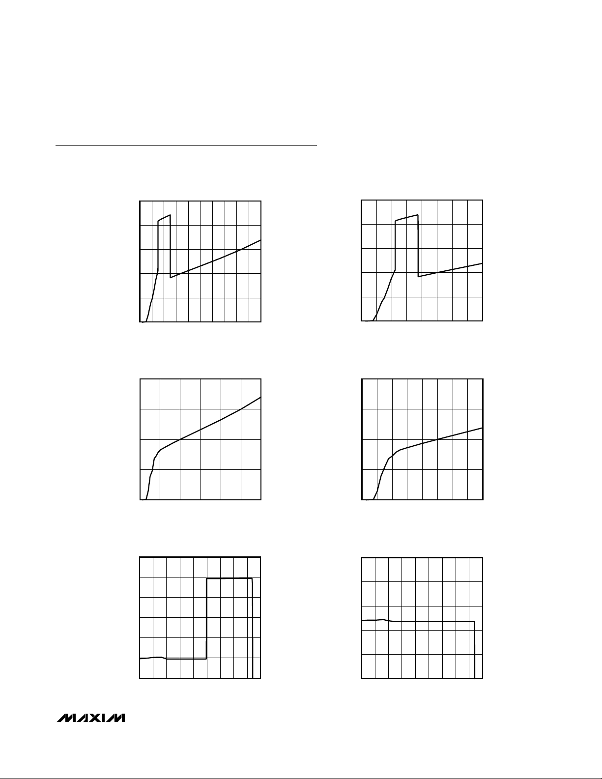
Typical Operating Characteristics
(V
BAT
= 3.6V; DC charge mode: VDC= 5V, V
USB
= 0V, V
DETBAT
= 0V (only for MAX8804W), V
SET
= 0V or unconnected; USB charge
mode: V
USB
= 5V, VDC= 0V, V
SET
= 5V; TA= +25°C, unless otherwise noted.)
STANDBY-MODE SUPPLY CURRENT
vs. INPUT VOLTAGE (USB CHARGING MODE)
INPUT VOLTAGE (V)
SUPPLY CURRENT (mA)
MAX8804Y/Z toc04
0246810121416
0
0.2
0.4
0.6
0.8
CHARGE CURRENT vs. BATTERY VOLTAGE
(DC CHARGING MODE)
BATTERY VOLTAGE (V)
CHARGE CURRENT (mA)
MAX8804Y/Z toc05
0 0.5 1.0 1.5 2.0 2.5 3.0 3.5 4.0 4.5
0
100
200
300
400
500
600
CHARGE CURRENT vs. BATTERY VOLTAGE
(USB CHARGING MODE)
BATTERY VOLTAGE (V)
CHARGE CURRENT (mA)
MAX8804Y/Z toc06
0 0.5 1.0 1.5 2.0 2.5 3.0 3.5 4.0 4.5
0
40
80
120
160
200
SUPPLY CURRENT vs. INPUT VOLTAGE
1.0
0.8
0.6
0.4
SUPPLY CURRENT (mA)
0.2
0
036912151821242730
DISABLED-MODE SUPPLY CURRENT
vs. INPUT VOLTAGE (DC CHARGING MODE)
0.8
0.6
(DC CHARGING MODE)
MAX8804Y/Z toc01
INPUT VOLTAGE (V)
MAX8804Y/Z toc03
SUPPLY CURRENT vs. INPUT VOLTAGE
1.0
0.8
0.6
0.4
SUPPLY CURRENT (mA)
0.2
0
(USB CHARGING MODE)
MAX8804Y/Z toc02
0246810121416
INPUT VOLTAGE (V)
SUPPLY CURRENT (mA)
0.4
0.2
0
0 5 10 15 20 25 30
INPUT VOLTAGE (V)
CHARGE CURRENT
vs. AMBIENT TEMPERATURE
AMBIENT TEMPERATURE (°C)
CHARGE CURRENT (mA)
MAX8804Y/Z toc13
-40 -15 10 35 60 85
200
300
400
500
600
700
DC CHARGE MODE 650mA
BATTERY REGULATION VOLTAGE
vs. LOAD CURRENT
LOAD CURRENT (mA)
BATTERY REGULATION VOLTAGE (V)
MAX8804Y/Z toc14
0 100 200 300 400 500 600 700
4.10
4.15
4.20
4.25
4.30
550mA CHARGE-CURRENT SETTING
BATTERY REGULATION VOLTAGE
vs. AMBIENT TEMPERATURE
AMBIENT TEMPERATURE (°C)
BATTERY REGULATION VOLTAGE (V)
MAX8804Y/Z toc12
-40 -15 10 35 60 85
4.180
4.186
4.192
4.198
4.204
4.210
USB MODE
DC MODE
MAX8804W/MAX8804Y/MAX8804Z
High-Voltage, Dual-Input, USB/AC
Adapter Chargers in 2mm x 3mm TDFN
6 _______________________________________________________________________________________
Typical Operating Characteristics (continued)
(V
BAT
= 3.6V; DC charge mode: VDC= 5V, V
USB
= 0V, V
DETBAT
= 0V (only for MAX8804W), V
SET
= 0V or unconnected; USB charge
mode: V
USB
= 5V, VDC= 0V, V
SET
= 5V; TA= +25°C, unless otherwise noted.)
CHARGE CURRENT
vs. DC INPUT VOLTAGE
600
120
CHARGE CURRENT
vs. USB INPUT VOLTAGE
CHARGE CURRENT vs. SET PULSE
(USB CHARGING MODE) (MAX8804Y/MAX8804Z)
MAX8804Y/Z toc09
500
400
300
200
CHARGE CURRENT (mA)
100
0
0 5 10 15 20 25 30
INPUT VOLTAGE (V)
CHARGE CURRENT vs. SET PULSE
(DC CHARGING MODE) (MAX8804Y/MAX8804Z)
V
SET
700mA
I
CHG
500mA
550mA
600mA
450mA
650mA
400mA
MAX8804Y/Z toc10
700mA
2ms/div
500mA
MAX8804Y/Z toc07
1V/div
200mA/div
90
60
CHARGE CURRENT (mA)
30
0
0246810121416
INPUT VOLTAGE (V)
CHARGE CURRENT
vs. INPUT VOLTAGE HEADROOM
600
INPUT VOLTAGE DECREASING
500
400
300
200
CHARGE CURRENT (mA)
100
0
0 100 200 300 400 500
INPUT VOLTAGE HEADROOM (mV)
DC MODE
USB MODE
V
MAX8804Y/Z toc08
I
CHG
MAX8804Y/Z toc11
SET
475mA
475mA
380mA 380mA
95mA 95mA
2ms/div
1V/div
475mA
200mA/div
95mA

MAX8804W/MAX8804Y/MAX8804Z
High-Voltage, Dual-Input, USB/AC
Adapter Chargers in 2mm x 3mm TDFN
_______________________________________________________________________________________ 7
Pin Description
PIN
MAX8804W
1 1 BAT
2 — DETBAT
—2USBPWR
33POK
44DC
5 5 USB
66CHG
7 7 SET
8 8 GND Ground
— — EP Exposed Paddle. Connect to the GND plane for optimum thermal dissipation.
MAX8804Y/
MAX8804Z
NAME FUNCTION
Battery Connection. The IC delivers charging current and monitors battery voltage
using BAT. Bypass BAT to GND with a 2.2µF or larger ceramic capacitor. BAT is high
impedance when the IC is disabled.
Battery Pack Detection Input. Drive DETBAT low or connect it to GND to allow SET to
control the charger. Leave DETBAT unconnected to disable any charge mode.
USB Input Detection Output. USBPWR is internally pulled low if a valid voltage is
present at USB, otherwise it is high impedance. USBPWR circuitry is active regardless
of SET and charger on/off status.
Power-OK Monitor. POK is an open-drain output that is internally pulled low when a
valid charging source is detected at either DC or USB. POK is high impedance when
both input voltages are less than V
DC Input Supply. Connect DC to a 4.15V to 7V charging source. Bypass DC to GND
with a 1µF or larger ceramic capacitor. DC takes priority over USB when both are valid.
USB Input Source. Connect USB to a USB port. Bypass USB to GND with a 1µF or
larger ceramic capacitor.
Charging-Status Output. CHG is internally pulled low when the battery is being
charged. CHG is high impedance when the charger is in top-off mode or disabled.
Enable/Disable, Charging Current, and Top-Off Threshold Set Input. Drive SET low to
enable DC charge mode and drive high to enable USB charge mode. If both DC and
USB inputs are present, SET is used for the DC charge mode only and USB charge is
disabled. SET is also used for programming the charge current and top-off threshold.
See the DC/USB Mode and Charging Current Setting section for details.
UVLO
or V
BAT
.

MAX8804W/MAX8804Y/MAX8804Z
High-Voltage, Dual-Input, USB/AC
Adapter Chargers in 2mm x 3mm TDFN
8 _______________________________________________________________________________________
Detailed Description
The MAX8804W/MAX8804Y/MAX8804Z dual-input linear
battery chargers use voltage, current, and thermal-control loops to charge and protect a single Li+ battery.
When a Li+ battery with a cell voltage below 2.5V is
inserted, the MAX8804W/MAX8804Z chargers enter the
prequalification stage where they precharge that cell
with 95mA (Figure 2). The CHG indicator output is driven low to indicate entry into the prequalification state.
When battery voltage exceeds 2.5V, the charger softstarts as it enters the fast-charge stage. The MAX8804Y
eliminates the prequalification state and enters fastcharge when the battery is inserted. The fast-charge current level is programmed by a simple single-wire
interface. As the battery voltage approaches 4.2V, the
charging current is reduced. If the battery current drops
below the top-off current threshold, the CHG indicator
goes high impedance, signaling that the battery is fully
charged. The ICs then enter a constant voltage-regulation mode to maintain the battery at full charge.
The MAX8804W/MAX8804Y/MAX8804Z automatically
select between either a USB or AC adapter input source.
The AC adapter charge current is programmable from
400mA to 700mA in 50mA steps through a simple singlewire interface (see Tables 2 and 3). The USB charge current is programmable to 95mA, 380mA, or 475mA
through the same interface (see Tables 4 and 5).
Figure 1. Functional Diagram
4.15V TO 30V
4.15V TO 16V
USB
DC
MAX8804Y
MAX8804Z
DC
POK
USB
POK
DC AND USB OUTPUT CONTROL
VOLTAGE
LOGIC
CONTROL
BAT
Li+
+105°C
TEMP
SENSOR
LOOP
OVERVOLTAGE
PROTECTION
(DETBAT)
SET
CHG
POK
<USBPWR>
REF
BIAS
CIRCUIT
GND
NOTE: ( ) FOR MAX8804W ONLY
< > FOR MAX8804Y/MAX8804Z ONLY

MAX8804W/MAX8804Y/MAX8804Z
High-Voltage, Dual-Input, USB/AC
Adapter Chargers in 2mm x 3mm TDFN
_______________________________________________________________________________________ 9
DC Charging
The MAX8804W/MAX8804Y/MAX8804Z are designed
to charge a single-cell Li+ battery from a DC source
voltage between 4.15V and 7V and withstand up to 30V
maximum input voltage. The charge current and top-off
threshold are programmed with the SET input.
USB Charging
The MAX8804W/MAX8804Y/MAX8804Z contain a USB
input that allows operation from a USB port with voltages
between 4.15V and 7V and can withstand up to 16V maximum input voltage. Pulsing SET allows programming a
95mA, 380mA, or 475mA maximum charging current
when using the USB input.
Figure 2. Charger State Diagram
ASYNCHRONOUS
FROM ANYWHERE
= HIGH > 2ms
t
SET
FOR DC MODE
= LOW > 2ms
t
SET
FOR USB MODE
< 2.5V
V
BAT
STANDBY MODE
CHARGER = OFF
POK = LOW
CHG = HIGH IMPEDANCE
t
SET
POK = LOW
CHG = LOW
FOR DC MODE
t
SET
FOR USB MODE
MAX8804W/
MAX8804Z
PREQUALIFICATION
DEFAULT CHARGE CURRENT
V
< 2.2V
BAT
MAX8804W/
MAX8804Z
= LOW > 2ms
= HIGH > 2ms
> 2.5V
V
BAT
< VIN < V
V
UVLO
AND VIN > V
BAT
OVP
SHUTDOWN
CHARGER = OFF
POK = HIGH IMPEDANCE*
CHG = HIGH IMPEDANCE
VIN < V
OR V
OR V
OR DETBAT = HIGH
MAX8804Y
= LOW > 2ms
t
SET
FOR DC MODE
= HIGH > 2ms
t
SET
FOR USB MODE
IN
BAT
UVLO
> V
> V
OVP
ASYNCHRONOUS
FROM ANYWHERE
< V
V
IN
IN
OR VIN > V
OR V
BAT
OR DETBAT = HIGH
UVLO
> V
OVP
IN
FAST-CHARGE
100% CHARGE CURRENT
POK = LOW
CHG = LOW
I
> I
TOP-OFF
+ 57mA FOR ALL
I
CHG
FULL BAT
= 4.2V
V
BAT
POK = LOW
CHG = HIGH IMPEDANCE
< I
TOP-OFF
CHG
FAST-CHARGE OPTIONS EXCEPT 95mA
CV MODE TO CC MODE FOR 95mA
FAST-CHARGE OPTION
*POK = LOW WHEN VIN > V
OVP

MAX8804W/MAX8804Y/MAX8804Z
High-Voltage, Dual-Input, USB/AC
Adapter Chargers in 2mm x 3mm TDFN
10 ______________________________________________________________________________________
DC/USB Mode and
Charging Current Setting
SET is a logic input that sets DC/USB charging mode
and charging current. Drive SET low or leave it unconnected to enable DC charging mode. Drive SET high to
enable USB charging mode (see Table 1). SET can
also be driven by series pulses to program the charging current in both DC and USB mode.
DC Charge Mode
Drive SET low or leave it unconnected to enable DC
charging mode. Subsequent pulses on SET program
the charging current and the top-off threshold. There
are seven fast-charge current options and four top-off
threshold options. Default fast-charge current and topoff threshold current are 500mA and 80mA. Pulse SET
high (1µs to 1ms pulse width) subsequently to realize
charging current and top-off threshold programming
and transition. After the 28th pulse, the MAX8804W/
MAX8804Y/MAX8804Z go into the default mode and
start a new cycle. See Tables 2 and 3 and Figure 3 to
set the desired charging current and top-off threshold.
Drive SET high longer than 2ms to disable the DC
charging-control circuitry.
Table 1. SET Truth Table
Table 2. MAX8804Y/MAX8804Z DC Charging Current Programming by Series Pulses
Table 3. MAX8804W DC Charging Current Programming by Series Pulses
Note: This table is true when DETBAT = LOW for the MAX8804W.
When DETBAT = HIGH, the MAX8804W enters shutdown.
SET V
0 Invalid Invalid Off
0 Invalid Valid Off
0 Valid Invalid
0 Valid Valid
1 Invalid Invalid Off
1 Invalid Valid
1 Valid Invalid Off
1 Valid Valid Off
DC
V
USB
CHARGER STATUS
DC charging mode enabled,
USB charging mode disabled
DC charging mode enabled,
USB charging mode disabled
DC charging mode disabled,
USB charging mode enabled
PULSE
NUMBER
I
(mA) 500 500 500 500 550 550 550 550 600 600 600 600 450 450 450
CHG
Top - O ff C ur r ent
Thr eshol d ( m A)
PULSE
NUMBER
I
(mA) — 450 400 400 400 400 650 650 650 650 700 700 700 700 500
CHG
Top - O ff C ur r ent
Thr eshol d ( m A)
DEFAULT 1st 2nd 3rd 4th 5th 6th 7th 8th 9th 10th 11th 12th 13th 14th
80 90 100 70 80 90 100 70 80 90 100 70 80 90 100
— 15th 16th 17th 18th 19th 20th 21st 2 2 n d 2 3 r d 24th 25th 26th 27th 28th
— 70 80 90 100 70 80 90 100 70 80 90 100 70 80
PULSE
NUMBER
I
(mA) 450 450 450 450 550 550 550 550 500 500 500 500 400 400 400
CHG
Top - O ff C ur r ent
Thr eshol d ( m A)
PULSE
NUMBER
I
(mA) — 400 600 600 600 600 650 650 650 650 700 700 700 700 450
CHG
Top - O ff C ur r ent
Thr eshol d ( m A)
DEFAULT 1st 2nd 3rd 4th 5th 6th 7th 8th 9th 10th 11th 12th 13th 14th
80 90 100 70 80 90 100 70 80 90 100 70 80 90 100
— 15th 16th 17th 18th 19th 20th 21st 2 2 n d 2 3 r d 24th 25th 26th 27th 28th
— 70 80 90 100 70 80 90 100 70 80 90 100 70 80

MAX8804W/MAX8804Y/MAX8804Z
High-Voltage, Dual-Input, USB/AC
Adapter Chargers in 2mm x 3mm TDFN
______________________________________________________________________________________ 11
USB Charge Mode
Drive SET high to enable USB charging mode when the
USB input is valid. Subsequent low pulses with 1µs to
1ms pulse width on SET program the fast charging current from 95mA, 380mA, to 475mA and then repeat
new cycle as shown in Tables 4 and 5. Drive SET low or
leave it unconnected longer than 2ms to disable USB
charging-control circuitry.
Table 4. MAX8804Y/MAX8804Z USB
Charging Current Programming by Series
Pulses
POK
Figure 3. DC Charging Current and Top-Off Threshold Programming
Table 5. MAX8804W USB Charging
Current Programming by Series Pulses
SET
I
CHG
DC
234 2425262728
1
> 2ms
t
HIGH
2ms
DELAY
0mA
t
SOFTSTART
500mA
(450mA)
550mA
(550mA)
700mA
(700mA)
500mA
(450mA)
0mA
TOP-OFF
CURRENT
THRESHOLD
NOTE: ( ) FOR MAX8804W
80mA
90mA
100mA
70mA
80mA
100mA
80mA
90mA
70mA
80mA
PULSE NUMBER DEFAULT 1st 2nd 3rd
I
(mA) 95 380 475 95
CHG
Top-Off Current
Threshold (mA)
80 80 80 80
PULSE NUMBER DEFAULT 1st 2nd 3rd
I
(mA) 380 475 95 380
CHG
Top-Off Current
Threshold (mA)
80 80 80 80

MAX8804W/MAX8804Y/MAX8804Z
High-Voltage, Dual-Input, USB/AC
Adapter Chargers in 2mm x 3mm TDFN
12 ______________________________________________________________________________________
Soft-Start
The soft-start circuitry activates when entering fastcharge mode. In the MAX8804Y, soft-start is entered
directly after being enabled, and the charging current
ramps up in 250µs from 0 to 500mA (95mA in USB
mode). This reduces the inrush current on the input
supply. Note that the MAX8804W/MAX8804Z has a prequalification state and the charging current ramps up
when the prequalification state is complete (V
BAT
exceeds 2.5V).
Thermal Regulation Control
The thermal-regulation loop limits the MAX8804W/
MAX8804Y/MAX8804Z die temperature to +105°C by
reducing the charge current as necessary. This feature
not only protects the ICs from overheating, but also
allows a higher charge current at room temperature
without risking damage to the system.
Charging-Status Output (
CHG
)
CHG is an open-drain output that indicates charger status. CHG goes low during charge cycles where the
MAX8804W/MAX8804Y/MAX8804Z are in prequalification or fast-charge mode. CHG goes high impedance
when the charge current reaches the top-off threshold
for more than 4ms, indicating charging is done. The
CHG status is latched after the top-off threshold is
reached. The latch is reset by toggling the SET input,
recycling input power, or increasing the charging current to the top-off threshold plus 57mA (typ).
When the MAX8804W/MAX8804Y/MAX8804Z are used
in conjunction with a microprocessor (µP), connect a
pullup resistor between CHG and the logic I/O voltage
to indicate charge status to the µP. Alternatively, CHG
can sink up to 5mA for an LED charge indicator.
Figure 4. USB Charging Current Programming
USB
POK
USBPWR
1
SET
t
LOW
2ms
t
SOFTSTART
DELAY
MAX8804Y/
MAX8804Z
I
CHG
0mA
MAX8804W
I
CHG
0mA
TOP-OFF
CURRENT
THRESHOLD
95mA
380mA
380mA
475mA
2
475mA
95mA
80mA
3
95mA
380mA
> 2ms
0mA
0mA

MAX8804W/MAX8804Y/MAX8804Z
High-Voltage, Dual-Input, USB/AC
Adapter Chargers in 2mm x 3mm TDFN
______________________________________________________________________________________ 13
Power-OK Monitor (
POK
)
The MAX8804W/MAX8804Y/MAX8804Z contain an
open-drain POK output that goes low when a valid input
source is detected at either DC or USB. A valid input
source is one whose voltage is greater than 4.15V and
exceeds the battery voltage by 250mV. After a valid
input has been established, charging is sustained with
inputs as low as 3.5V as long as the input voltage
remains above the battery voltage by at least 40mV.
POK status is maintained regardless of SET status.
When the MAX8804W/MAX8804Y/MAX8804Z are used
in conjunction with a µP, connect a pullup resistor
between POK and the logic I/O voltage to indicate
power-OK to the µP. Alternatively, POK can sink up to
5mA for an LED power-OK indicator.
USB Power Status Output (
USBPWR
)
(MAX8804Y/MAX8804Z Only)
USBPWR is internally pulled low when V
USB
> V
UVLO
and V
USB
- V
BAT
> 250mV. Otherwise, it is high imped-
ance. USBPWR indicates the USB input presence
regardless of SET status and charger status.
When the MAX8804Y/MAX8804Z are used in conjunction
with a µP, connect a pullup resistor between USBPWR
and the logic I/O voltage to indicate USB power status
to the µP. Alternatively, USBPWR can sink up to 5mA
for an LED USB power status indicator.
Battery Pack Dectection Input
(DETBAT, MAX8804W Only)
DETBAT is pulled up to an internal 3V supply through a
63kΩ resistor. Driving DETBAT low or connecting it to
GND allows SET to control the charger. When DETBAT
is left unconnected, the MAX8804W enters shutdown.
Applications Information
Capacitor Selection
Connect a 2.2µF ceramic capacitor from BAT to GND for
proper stability. Connect a 1µF ceramic capacitor from
DC to GND. If using the USB input, bypass USB to GND
with a 1µF ceramic capacitor. Use a larger input bypass
capacitor for high charging currents to reduce supply
noise. All capacitors should be X5R dielectric or better.
Be aware that some capacitors have large voltage and
temperature coefficients and should be avoided.
Thermal Considerations
The MAX8804W/MAX8804Y/MAX8804Z are available in
a thermally enhanced TDFN package with an exposed
paddle. Connect the exposed paddle to a large copper
ground plane to provide a thermal contact between the
device and the PCB for increased power dissipation.
The exposed paddle transfers heat away from the
device, allowing the IC to charge the battery with maximum current, while minimizing the die temperature
increase.
Input Sources
The MAX8804W/MAX8804Y/MAX8804Z operate from
well-regulated input sources. The operating input voltage range is 4.15V to 7V. The device survives DC input
supply voltages up to 30V and USB input source voltages up to 16V without damage to the IC. If the input
voltage is greater than 7.5V (typ), the IC stops charging. An appropriate power supply must provide at least
4.2V plus the voltage drop across the internal pass
transistor when sourcing the desired maximum charging current:
V
IN(MIN)
> 4.2V + I
CHARGE(MAX)
x R
ON
where RONis the input-to-BAT resistance (typically
0.55Ω for DC or 0.65Ω for USB). Failure to meet this
requirement results in an incomplete charge or
increased charge time.
Application Circuits
Stand-Alone Li+ Charger
The MAX8804W/MAX8804Y/MAX8804Z provide a complete Li+ charging solution. The
Typical Application
Circuit
shows the MAX8804W/MAX8804Y/MAX8804Z as
a stand-alone Li+ battery charger. The LED indicates
when either fast-charge or prequalification has begun.
When the battery is fully charged, the LED turns off.
Microprocessor-Interfaced Li+ Charger
Figure 5 shows the MAX8804W/MAX8804Y/MAX8804Z
as a µP-interfaced Li+ battery charger. The µP drives
SET to enable/disable DC/USB mode charging. CHG
can be used to detect the charge status of a battery.
Layout and Bypassing
Connect the input capacitors as close as possible to
the IC. Provide a large copper GND plane to allow the
exposed paddle to sink heat away from the IC. Connect
the battery to BAT as close as possible to the IC to provide accurate battery voltage sensing. Make all highcurrent traces short and wide to minimize voltage
drops. A sample layout is available in the MAX8804Z
evaluation kit to speed designs.
MAX8804W/MAX8804Y/MAX8804Z
High-Voltage, Dual-Input, USB/AC
Adapter Chargers in 2mm x 3mm TDFN
14 ______________________________________________________________________________________
Figure 5. Microprocessor-Interfaced Li+ Charger with the MAX8804W/MAX8804Y/MAX8804Z
Chip Information
PROCESS: BiCMOS
1
+
34
865
GND CHG USB
MAX8804W
MAX8804Y
MAX8804Z
2
7
SET
BAT POK
DC
USBPWR
TDFN
2mm × 3mm
TOP VIEW
(DETBAT)
() FOR MAX8804W
Pin Configuration
SYSTEM I/O
AC
ADAPTER
USB PORT
1μF
1μF
Li+
2.2μF
DC
USB
(DETBAT)
BAT
MAX8804W
MAX8804Y
MAX8804Z
GND
CHG
POK
<USBPWR>
SET
NOTE: () FOR MAX8804W
<> FOR MAX8804Y/MAX8804Z
μP

MAX8804W/MAX8804Y/MAX8804Z
High-Voltage, Dual-Input, USB/AC
Adapter Chargers in 2mm x 3mm TDFN
______________________________________________________________________________________ 15
Package Information
(The package drawing(s) in this data sheet may not reflect the most current specifications. For the latest package outline information,
go to www.maxim-ic.com/packages
.)
8L, TDFN.EPS
PACKAGE OUTLINE
8L TDFN, EXPOSED PAD, 2x3x0.8mm
21-0174
1
B
2

MAX8804W/MAX8804Y/MAX8804Z
High-Voltage, Dual-Input, USB/AC
Adapter Chargers in 2mm x 3mm TDFN
16 ______________________________________________________________________________________
Package Information (continued)
(The package drawing(s) in this data sheet may not reflect the most current specifications. For the latest package outline information,
go to www.maxim-ic.com/packages
.)
SYMBOL
A
E
D
A1
L
k 0.20 MIN.
A2
e
b
MIN.
0.70
1.95
0.00
0.30
DIMENSIONS
NOM.
0.75
3.002.95
2.00
0.02
0.40
0.20 REF.
8N
0.50 BSC
0.250.18 0.30
MAX.
0.80
3.05
2.05
0.05
0.50
PKG.
CODE
T823-1
MIN.
1.60
EXPOSED PAD PACKAGE
E2
MAX.
1.90
MIN.
1.50
NOM.
1.75
D2
NOM.
1.63
MAX.
1.75
PACKAGE OUTLINE
8L TDFN, EXPOSED PAD, 2x3x0.8mm
21-0174
2
B
2

MAX8804W/MAX8804Y/MAX8804Z
High-Voltage, Dual-Input, USB/AC
Adapter Chargers in 2mm x 3mm TDFN
Maxim cannot assume responsibility for use of any circuitry other than circuitry entirely embodied in a Maxim product. No circuit patent licenses are
implied. Maxim reserves the right to change the circuitry and specifications without notice at any time.
Maxim Integrated Products, 120 San Gabriel Drive, Sunnyvale, CA 94086 408-737-7600 ____________________
17
© 2007 Maxim Integrated Products is a registered trademark of Maxim Integrated Products, Inc.
Heaney
Revision History
REVISION
NUMBER
0 4/07 Initial release. —
1 10/07 Added MAX8804W and Battery Pack Detection feature. 1–16
REVISION
DATE
DESCRIPTION
PAGES
CHANGED
 Loading...