General Description
The MAX8790 is a high-efficiency driver for white lightemitting diodes (LEDs). It is designed for large liquidcrystal displays (LCDs) that employ an array of LEDs as
the light source. A current-mode step-up controller drives
up to six parallel strings of multiple series-connected
LEDs. Each string is terminated with ballast that achieves
±1.5% current regulation accuracy, ensuring even brightness for all LEDs. The MAX8790 has a wide input-voltage
range from 4.5V to 26V, and provides a fixed 20mA or
adjustable 15mA to 25mA full-scale LED current.
The MAX8790 has two dimming control modes to
enable a wide variety of applications. In direct DPWM
mode, the LED current is directly turned on and off by a
PWM signal. In analog dimming mode, an internal
phase-locked loop (PLL) circuit translates the PWM signal into an analog signal and linearly controls the LED
current down to 12.5%. Below 12.5%, digital dimming is
added to allow lower average LED current down to 1%.
Both control methods provide 100:1 dimming range.
The MAX8790 has multiple features to protect the controller from fault conditions. Separate feedback loops limit
the output voltage if one or more LEDs fail open or short.
The controller features cycle-by-cycle current limit to provide consistent operation and soft-start capability. A thermal-shutdown circuit provides another level of protection.
The step-up controller uses an external MOSFET, which
provides good efficiency and allows for scalable output
power and maximum operating voltage. Low feedback
voltage at each LED string (450mV) helps reduce
power loss. The MAX8790 features selectable switching
frequency (500kHz, 750kHz, or 1MHz), which allows
trade-offs between external component size and operating efficiency.
The MAX8790 is available in a thermally enhanced,
lead-free, 20-pin, 4mm x 4mm, Thin QFN package.
Applications
Notebook, Subnotebook, and Tablet Computer
Displays
Automotive Systems
Handy Terminals
Features
o Drives Six Parallel Strings with Multiple Series-
Connected LEDs per String
o ±1.5% Current Regulation Accuracy Between
Strings
o Low 450mV Feedback Voltage at Full Current
Improves Efficiency
o Step-Up Controller Regulates the Output Just
Above the Highest LED String Voltage
o Full-Scale LED Current Adjustable from 15mA to
25mA, or Preset 20mA
o Wide 100:1 Dimming Range
o Programmable Dimming Control: Direct DPWM or
Analog Dimming
o Built-In PLL for Synchronized Dimming Control
o Open and Short LED Protections
o Output Overvoltage Protection
o Wide Input Voltage Range from 4.5V to 26V
o External MOSFET Allows a Large Number of LEDs
per String
o 500kHz/750kHz/1MHz Switching Frequency
o Small, 20-Pin, 4mm x 4mm Thin QFN Package
MAX8790
Six-String White LED Driver with Active
Current Balancing for LCD Panel Applications
________________________________________________________________
Maxim Integrated Products
1
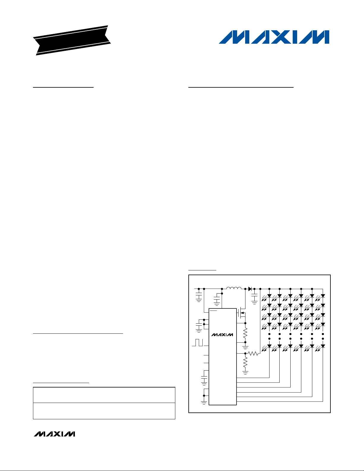
Simplified Operating Circuit
Ordering Information
19-0658; Rev 0; 11/06
For pricing, delivery, and ordering information, please contact Maxim/Dallas Direct! at
1-888-629-4642, or visit Maxim’s website at www.maxim-ic.com.
+
Denotes a lead-free package.
EVALUATION KIT
AVAILABLE
PART
TEMP RANGE
PIN-PACKAGE
PKG
CODE
MAX8790ETP+
20 Thin QFN
T2044-3
Pin Configuration appears at end of data sheet.
-40°C to +85°C
(4mm x 4mm)
V
D1
IN
MAX8790
GND
L1
EXT
CS
OV
FB1
FB2
FB3
FB4
FB5
FB6
V
IN
C
IN
0.1μF
SHDN
V
CC
FSET
ISET
BRT
N.C.
OSC
N.C.
CPLL
CCV
ENA
EP
OUT
N1
Rs
R1
R2
ABSOLUTE MAXIMUM RATINGS
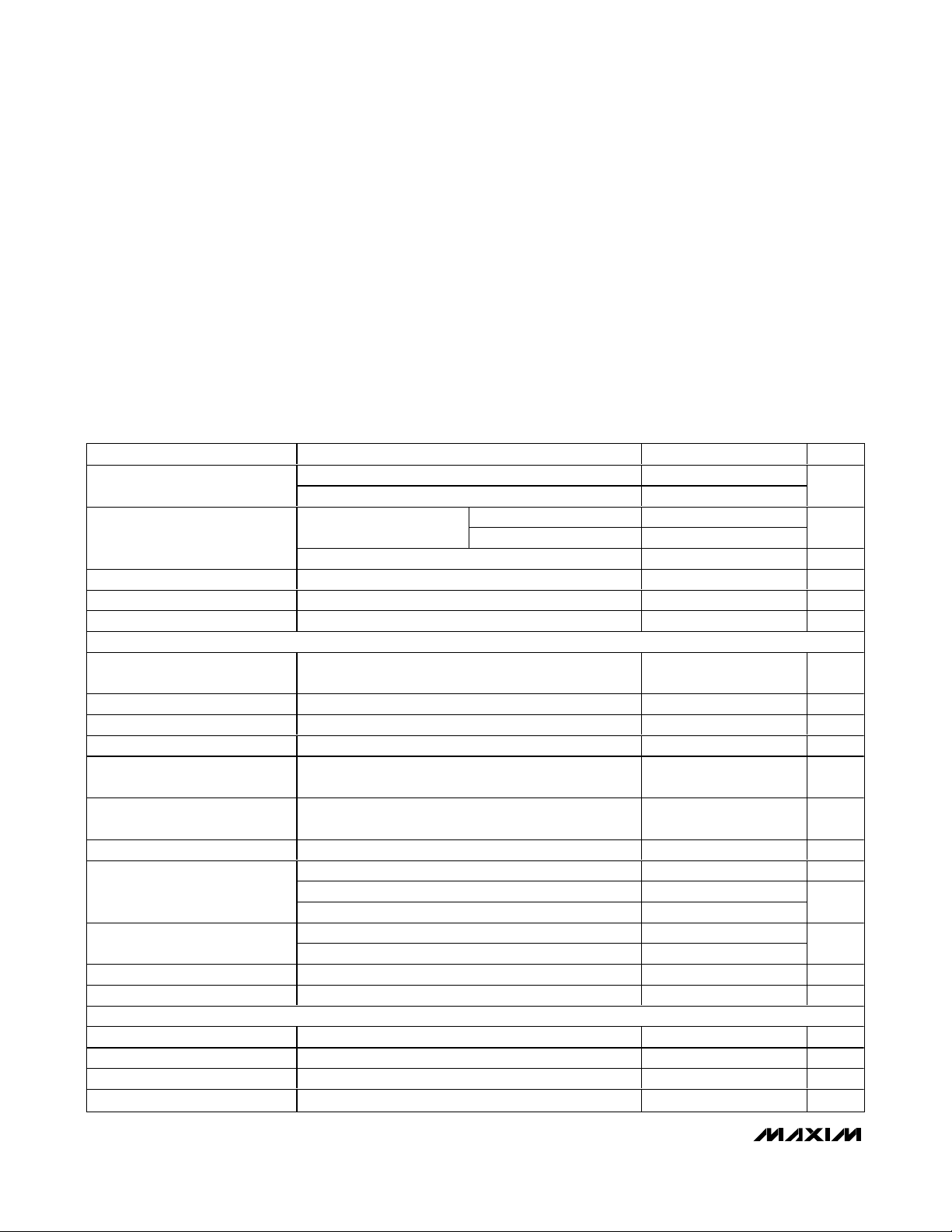
ELECTRICAL CHARACTERISTICS
(Circuit of Figure 1. VIN= 12V, V
SHDN
= VIN, CCV = 0.1µF, TA= 0°C to +85°C, unless otherwise noted. Typical values are at TA= +25°C.)
Stresses beyond those listed under “Absolute Maximum Ratings” may cause permanent damage to the device. These are stress ratings only, and functional
operation of the device at these or any other conditions beyond those indicated in the operational sections of the specifications is not implied. Exposure to
absolute maximum rating conditions for extended periods may affect device reliability.
IN, SHDN, to GND .................................................-0.3V to +28V
FB_ to GND ............................................................-0.3V to +28V
V
CC
, BRT, ENA, OSC, OV to GND ...........................-0.3V to +6V
ISET, CCV, CS, FSET, CPLL, EXT to GND .-0.3V to (V
CC
+ 0.3V)
Continuous Power Dissipation (T
A
= +70°C)
20-Pin Thin QFN (derate 16.9mW/°C above +70°C) ...1349mW
Operating Temperature Range ...........................-40°C to +85°C
Junction Temperature......................................................+150°C
Storage Temperature Range .............................-60°C to +150°C
Lead Temperature (soldering, 10s) .................................+300°C
MAX8790
Six-String White LED Driver with Active
Current Balancing for LCD Panel Applications
2 _______________________________________________________________________________________
PARAMETER CONDITIONS MIN TYP MAX UNITS
IN Input Voltage Range
IN Quiescent Current
VCC Output voltage V
VCC Short-Circuit Current 15 56 130 mA
VCC UVLO Threshold Rising edge, hysteresis = 20mV 4.00 4.25 4.45 V
STEP-UP CONVERTER
EXT High Level 10mA from EXT to GND
EXT Low Level -10mA from EXT to V
EXT On-Resistance EXT high or low 2 5 Ω
EXT Sink/Source Current EXT forced to 2V 1 A
OSC High-Level Threshold
OSC Midlevel Threshold 1.5
OSC Low-Level Threshold 0.4 V
Operating Frequency
Minimum Duty Cycle
Maximum Duty Cycle 94 95 %
CS Trip Voltage Duty cycle = 75% 85 100 115 mV
CONTROL INPUT
SHDN Logic-Input High Level 2.1 V
SHDN Logic-Input Low Level 0.8 V
BRT, ENA Logic-Input High Level 2.1 V
BRT, ENA Logic-Input Low Level 0.8 V
V
= V
IN
CC
V
= bypassed to GND through 1µF cap 5.5 26.0
CC
V
= high
SHDN
SHDN = GND
= 5V, 6V < VIN < 26V, 0 < I
SHDN
CC
V
= V
V
V
OSC
OSC
OSC
CC
= open 675 750 825
= GND 450 500 550
PWM mode 10
Pulse skipping, no load 0
4.5 5.5
VIN = 26V 1 2
= VCC = 5V 1 2
V
IN
10 µA
< 10mA 4.7 5.0 5.3 V
VCC
V
-
CC
0.1
V
CC
V
0 0.1 V
V
-
CC
0.4
V
VCC -
2.0
0.9 1.0 1.1 MHz
V
mA
V
kHz
%
MAX8790
Six-String White LED Driver with Active
Current Balancing for LCD Panel Applications
_______________________________________________________________________________________ 3
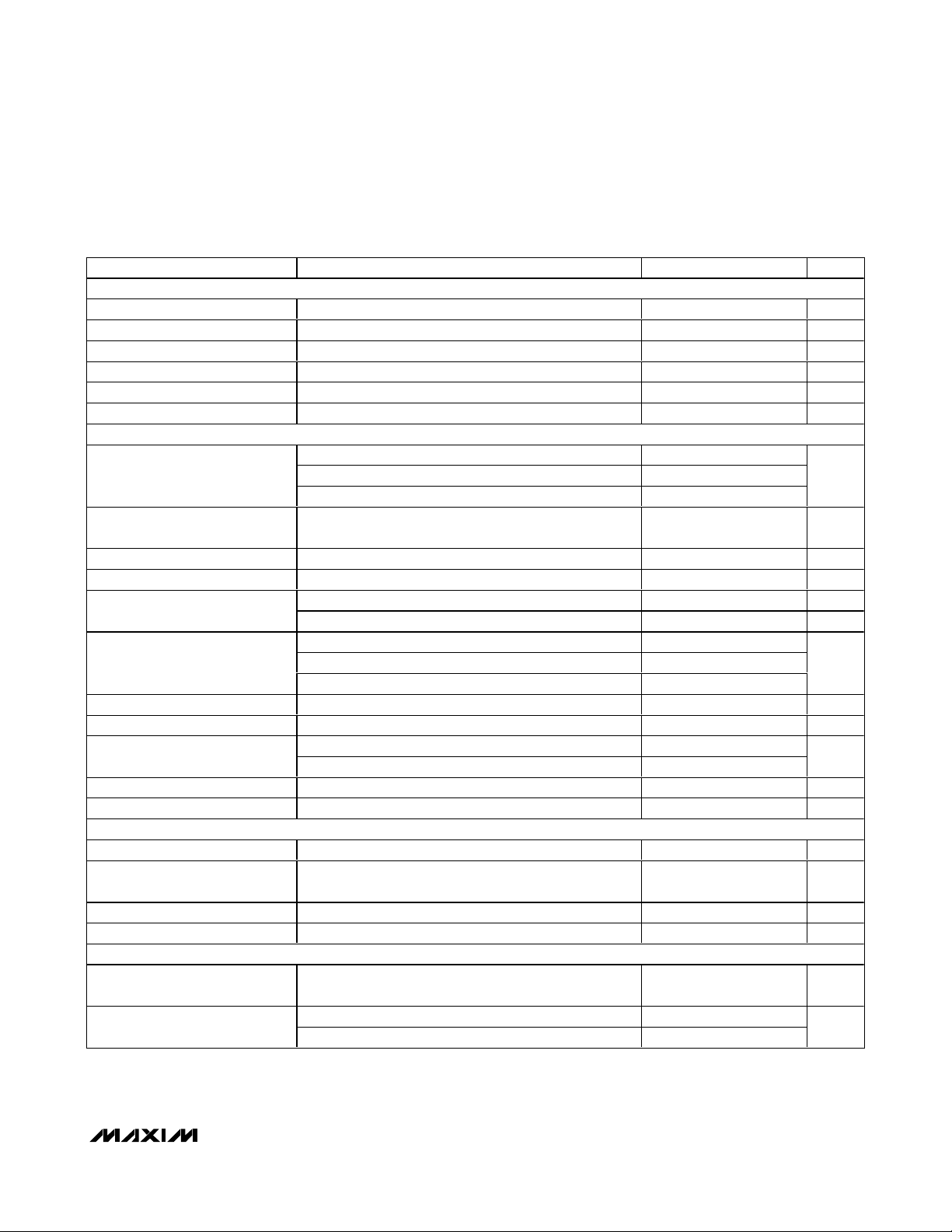
ELECTRICAL CHARACTERISTICS (continued)
(Circuit of Figure 1. VIN= 12V, V
SHDN
= VIN, CCV = 0.1µF, TA= 0°C to +85°C, unless otherwise noted. Typical values are at TA= +25°C.)
PARAMETER CONDITIONS MIN TYP MAX UNITS
INPUT LEAKAGE
SHDN Leakage Current SHDN = 26V +35 µA
CS Leakage Current VCS = GND +40 +50 µA
OSC Leakage Current -3 +3 µA
BRT, ENA Leakage Current -1 +1 µA
FSET, ISET Leakage Current FSET = ISET = V
OV Leakage Current -0.1 +0.1 µA
LED CURRENT
Full-Scale FB_ Output Current
ISET High-Level Threshold Default setting for 20mA full-scale LED current
ISET Voltage 1.12 1.19 1.26 V
20% Output Current ISET = VCC, BRT = 20% 3.84 4.00 4.16 mA
Current Regulation Between
Strings
Minimum FB_ Regulation Voltage
Maximum FB_ Ripple ISET = V
FB_ On-Resistance V
FB_ Leakage Current
BRT Input Frequency 100 500 Hz
Minimum BRT Duty Cycle PLL active 12.5 %
FAULT PROTECTION
OV Threshold Voltage 1.16 1.23 1.30 V
FB_ Overvoltage Threshold
FAULT Shutdown Timer V
Thermal-Shutdown Threshold (Note 1) 170 °C
PHASE-LOCKED LOOP
FSET High-Level Threshold PLL disabled
BRT Frequency Capture Range
CC
ISET = V
R
ISET
R
ISET
ISET = V
ISET = V
R
ISET
ISET = V
ISET = V
FB_
SHDN = GND, V
SHDN = V
FB_
R
FSET
R
FSET
, BRT = 100% 19.40 20.00 20.60
CC
= 80kΩ to GND, BRT = 100% 24.25 25.00 25.75
= 133kΩ to GND, BRT = 100% 14.40 15.00 15.60
, BRT = 100% -1.5 +1.5 %
CC
, BRT = 20% -2.0 +2.0 %
CC
= 80kΩ to GND, BRT = 100% 300 500 800
, BRT = 100% 270 450 720
CC
, 12.5% 150 275 500
CC
CC , COUT
= 50mV 13 20 Ω
IN
> 5.6V (typ) 50 65 80 ms
= 500kΩ 150 200 250
= 250kΩ 300 400 500
= 1µF, OSC = VCC (Note 1) 120 200 mV
= 26V 1
FB_
, BRT = GND, V
FB_
= 15V
-1 +1 µA
V
-
CC
0.4
V
10 28
VCC +
0.20
V
CC
0.4
V
+
CC
0.6
-
V
V
1.45
CC
+
mA
mV
P-P
µA
V
Hz
MAX8790
Six-String White LED Driver with Active
Current Balancing for LCD Panel Applications
4 _______________________________________________________________________________________
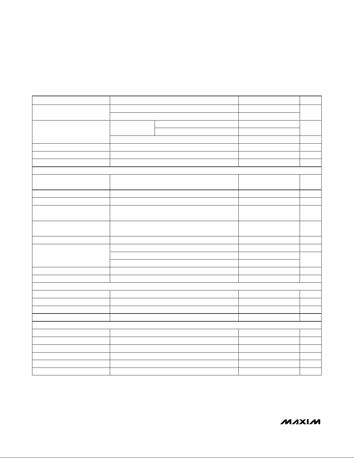
ELECTRICAL CHARACTERISTICS
(Circuit of Figure 1. VIN= 12V, V
SHDN
= VIN, CCV = 0.1µF, TA= -40°C to +85°C, unless otherwise noted.) (Note 2)
PARAMETER CONDITIONS MIN TYP MAX UNITS
IN Input Voltage Range
IN Quiescent Current
VCC Output Voltage V
VCC Short-Circuit Current 12 130 mA
VCC UVLO Threshold Rising edge, hysteresis = 20mV 4.00 4.45 V
STEP-UP CONVERTER
EXT High Level 10mA from EXT to GND
EXT Low Level -10mA from EXT to V
EXT On-Resistance EXT high or low 5 Ω
OSC High-Level Threshold
OSC Midlevel Threshold 1.5
OSC Low-Level Threshold 0.4 V
Maximum Duty Cycle 94 %
CS Trip Voltage Duty cycle = 75% 85 115 mV
CONTROL INPUT
SHDN Logic-Input High Level 2.1 V
SHDN Logic-Input Low Level 0.8 V
BRT, ENA Logic-Input High Level 2.1 V
BRT, ENA Logic-Input Low Level 0.8 V
INPUT LEAKAGE
SHDN Leakage Current SHDN = 26V +35 µA
CS Leakage Current VCS = GND +50 µA
OSC Leakage Current -3 +3 µA
BRT, ENA Leakage Current -1 +1 µA
FSET, ISET Leakage Current FSET = ISET = V
OV Leakage Current -0.1 +0.1 µA
V
= V
IN
CC
V
bypassed to GND through 1µF cap 5.5 26.0
CC
V
= high
SHDN
SHDN = GND
= 5V, 6V < VIN < 26V, 0 < I
SHDN
V
= V
V
V
OSC
OSC
OSC
CC
= open 675 825Operating Frequency
= GND 450 550
VIN = 26V 2
= VCC = 5V 2
V
IN
< 10mA 4.7 5.3 V
VCC
CC
CC
4.5 5.5
V
CC
0.1
V
CC
0.4
0.9 1.1 MHz
-1 +1 µA
10 µA
-
V
0.1 V
-
V
VCC -
2.0
V
mA
V
kHz
MAX8790
Six-String White LED Driver with Active
Current Balancing for LCD Panel Applications
_______________________________________________________________________________________ 5
Note 1: Specifications are guaranteed by design, not production tested.
Note 2: Specifications to -40°C are guaranteed by design, not production tested.
ELECTRICAL CHARACTERISTICS (continued)
(Circuit of Figure 1. VIN= 12V, V
SHDN
= VIN, CCV = 0.1µF, TA= -40°C to +85°C, unless otherwise noted.) (Note 2)
PARAMETER CONDITIONS MIN TYP MAX UNITS
LED CURRENT
ISET High-Level Threshold Default setting for 20mA full-scale LED current
ISET Voltage 1.12 1.26 V
20% Output Current ISET = VCC, BRT = 20% 3.8 4.2 mA
Current Regulation Between
Strings
Maximum FB_ Ripple ISET= VCC, C
FB_ On-Resistance V
FB_ Leakage Current
BRT Input Frequency 100 500 Hz
FAULT PROTECTION
OV Threshold Voltage 1.16 1.30 V
FB_ Overvoltage Threshold
FAULT Shutdown Timer V
ISET = V
R
ISET
R
ISET
ISET = V
ISET = V
R
ISET
ISET= V
ISET = V
FB_
SHDN = GND, V
SHDN = V
FB_
, BRT = 100% 19.2 20.8
CC
= 80kΩ to GND, BRT = 100% 24.0 26.0Full-Scale FB_ Output Current
= 133kΩ to GND, BRT = 100% 14.4 15.6
V
CC
0.4
, BRT = 100% -2 +2
CC
, BRT = 20% -3 +3
CC
= 80kΩ to GND, BRT = 100% 280 840
, BRT = 100% 250 760Minimum FB_ Regulation Voltage
CC
, BRT = 12.5% 140 530
CC
= 1µF, OSC = VCC (Note 1) 200 mV
OUT
= 50mV 20 Ω
= 26V 1
FB_
, BRT = GND, V
IN
> 5.6V (typ) 50 80 ms
= 15V 28
FB_
V
CC
0.2
-
V
+
VCC +
1.45
PHASE-LOCKED LOOP
V
-
FSET High-Level Threshold PLL disabled
R
= 500kΩ 150 250 Hz
BRT Frequency Capture Range
FSET
R
= 250kΩ 300 500 Hz
FSET
CC
0.4
V
mA
%
mV
P-P
µA
V
MAX8790
Six-String White LED Driver with Active
Current Balancing for LCD Panel Applications
6 _______________________________________________________________________________________
Typical Operating Characteristics
(Circuit configuration 1, VIN= 12V, V
SHDN
= VIN, LEDs = 8 series x 6 parallel strings, ISET = VCC, TA= +25°C, unless otherwise noted.)
BOOST CONVERTER EFFICIENCY
vs. INPUT VOLTAGE (BRT = 100%)
MAX8790 toc01
BOOST CONVERTER EFFICIENCY (%)
INPUT VOLTAGE (V)
94
93
92
91
90
89
88
87
86
71217
500kHz
750kHz
1MHz
NORMALIZED POWER vs. TOTAL LED CURRENT
(ANALOG AND DPWM DIMMING)
MAX8790 toc02
NORMALIZED POWER
TOTAL LED CURRENT (mA)
1.2
1.0
0.8
0.6
0.4
0.2
0
1 10 100 1000
NORMALIZED TO VIN = 20V, AND I
LED
= 20mA
V
IN
= 7V
TOTAL LED
POWER, ANALOG
TOTAL INPUT
POWER, DPWM
TOTAL INPUT
POWER, ANALOG
TOTAL LED
POWER, DPWM
LED CURRENT vs. BRT DUTY CYCLE
(BRT AT 200Hz)
MAX8790 toc03
LED CURRENT (mA)
BRT DUTY CYCLE (%)
25
20
15
10
5
0
1 10 100
IDENTICAL FOR DPWM DIMMING
AND ANALOG DIMMING
LED CURRENT
vs. AMBIENT TEMPERATURE (BRT = 100%)
MAX8790 toc04
LED CURRENT (mA)
AMBIENT TEMPERATURE (°)
21.0
20.8
20.6
20.4
20.2
20.0
19.8
19.6
19.4
19.2
19.0
020 6040 80
LED CURRENT REGULATION
vs. INPUT VOLTAGE
MAX8790 toc05
LED CURRENT REGULATION (%)
INPUT VOLTAGE (V)
0.05
0.04
0.03
0.02
0.01
0
-0.01
-0.02
-0.03
-0.04
-0.05
71217
ANALOG DIMMING
BRT = 10%
DPWM DIMMING
BRT = 100%
DPWM DIMMING
BRT = 10%
FB_ VOLTAGE vs. LED CURRENT
(ANALOG DIMMING)
MAX8790 toc06
FB_ REGULATION VOLTAGE (V)
LED STRING CURRENT (mA)
0.7
0.6
0.5
0.4
0.3
0.2
0.1
0
0 5 10 15 20 25 30
SUPPLY CURRENT vs. INPUT VOLTAGE
(DPWM DIMMING)
MAX8790 toc07
SUPPLY CURRENT (mA)
INPUT VOLTAGE (V)
7
6
5
4
3
2
1
0
71217
BRT = 100%
BRT = 0%
SHUTDOWN CURRENT vs. INPUT VOLTAGE
MAX8790 toc08
SHUTDOWN CURRENT (μA)
INPUT VOLTAGE (V)
7
6
5
4
3
2
1
0
71217
SWITCHING WAVEFORMS
(BRT = 100%)
MAX8790 toc09
200ns/div
I
L
500mA/div
0mA
V
LX
10V/div
0V
MAX8790
Six-String White LED Driver with Active
Current Balancing for LCD Panel Applications
_______________________________________________________________________________________
7
Typical Operating Characteristics (continued)
(Circuit configuration 1, VIN= 12V, V
SHDN
= VIN, LEDs = 8 series x 6 parallel strings, ISET = VCC, TA= +25°C, unless otherwise noted.)
SWITCHING WAVEFORMS
(BRT = 15%, ANALOG DIMMING)
1μs/div
MAX8790 toc10
LED CURRENT WAVEFORMS
(BRT = 1% AT 200Hz, DPWM DIMMING)
LED CURRENT WAVEFORMS
(BRT = 50% AT 200Hz, DPWM DIMMING)
2ms/div
MAX8790 toc14
MAX8790 toc12
0V
0V
V
LX
10V/div
0V
I
L
500mA/div
0mA
STARTUP WAVEFORMS
(BRT = 100%, DPWM DIMMING)
4ms/div
MAX8790 toc13
BRT
5V/div
0V
V
FB1
5V/div
0V
MAX8790 toc11
SHDN
5V/div
0V
V
OUT
20V/div
0V
V
CCV
2V/div
0V
I
L
1A/div
0A
LED CURRENT WAVEFORMS
(BRT = 50% AT 200Hz, ANALOG DIMMING)
BRT
5V/div
V
FB1
1V/div
0V
0V
0mA
0A
BRT
5V/div
V
FB1
5V/div
I
LED
100mA/div
I
L
1A/div
1ms/div
LED CURRENT WAVEFORMS
(BRT = 1% AT 200Hz, ANALOG DIMMING)
1ms/div
MAX8790 toc15
0mA
0A
0V
0V
0mA
0mA
I
LED
100mA/div
I
L
1A/div
BRT
5V/div
V
FB1
2V/div
I
LED
50mA/div
I
L
500mA/div
1ms/div
LED-OPEN FAULT PROTECTION
(BRT = 100%, LED OPEN ON FB3)
20ms/div
MAX8790 toc16
0mA
0A
0V
0V
0V
0A
I
LED
50mA/div
I
L
1A/div
V
FB3
1V/div
V
FB1
10V/div
V
OUT
20V/div
I
L
1A/div
MAX8790
Six-String White LED Driver with Active
Current Balancing for LCD Panel Applications
8 _______________________________________________________________________________________
Typical Operating Characteristics (continued)
(Circuit configuration 1, VIN= 12V, V
SHDN
= VIN, LEDs = 8 series x 6 parallel strings, ISET = VCC, TA= +25°C, unless otherwise noted.)
LED-SHORT FAULT PROTECTION
(BRT = 100%, 2 LEDs SHORT ON FB3)
10ms/div
0A
V
FB3
1V/div
V
FB1
10V/div
V
OUT
20V/div
I
L
1A/div
0V
0V
0V
MAX8790 toc17
LED CURRENT BALANCING
vs. INPUT VOLTAGE (BRT = 100%)
MAX8790 toc18
LED CURRENT BALANCING ACCURACY (%)
INPUT VOLTAGE (V)
1.00
0.90
0.80
0.70
0.60
0.50
0.40
0.30
0.20
0.10
0
71217
750kHz
500kHz
1MHz
Pin Description
PIN NAME FUNCTION
1 OSC
2 ENA
3 BRT
4 SHDN
5 FB1
6 FB2
7 FB3
8 GND Ground
9 FB4
10 FB5
O sci l l ator Fr eq uency S el ecti on P i n. C onnect OS C to V
1M H z. C onnect O S C to G N D to set the fr eq uency to 500kH z. Fl oat OS C to set the fr eq uency to 750kH z.
Anal og D i m m i ng E nab l e. E N A sets the P WM contr ol m od e. S et E N A LOW to enab l e d i r ect D P WM d i m m i ng .
S et E N A H IGH to enab l e anal og d i m m i ng . In b oth m od es, the d uty cycl e of the P WM si g nal at the BRT i np ut
contr ol s the LE D cur r ent char acter i sti cs. S ee the D i m m i ng C ontr ol secti on for a com p l ete d escr i p ti on.
Brightness Control Input. The duty cycle of this digital input signal controls the LED current characteristics.
The allowable frequency range is 100Hz to 500Hz in analog dimming mode. The duty cycle can be 100%
to 1%. The BRT frequency can go above 500Hz in direct DPWM mode as long as the BRT pulse width is
greater than 50µs minimum. See the Dimming Control section for a complete description.
Shutdown Control Input. The MAX8790 shuts down when SHDN is less than 0.8V. Pulling SHDN above
2.1V enables the MAX8790. SHDN can be connected to the input voltage if desired.
LED String 1 Cathode Connection. FB1 is the open-drain output of an internal regulator, which controls
current through FB1. FB1 can sink up to 25mA. If unused, connect FB1 to GND.
LED String 2 Cathode Connection. FB2 is the open-drain output of an internal regulator, which controls
current through FB2. FB2 can sink up to 25mA. If unused, connect FB2 to GND.
LED String 3 Cathode Connection. FB3 is the open-drain output of an internal regulator, which controls
current through FB3. FB3 can sink up to 25mA. If unused, connect FB3 to GND.
LED String 4 Cathode Connection. FB4 is the open-drain output of an internal regulator, which controls
current through FB4. FB4 can sink up to 25mA. If unused, connect FB4 to GND.
LED String 5 Cathode Connection. FB5 is the open-drain output of an internal regulator, which controls
current through FB5. FB5 can sink up to 25mA. If unused, connect FB5 to GND.
to set the step - up conver ter ’ s osci l l ator fr eq uency to
C C
 Loading...