

Page 1
For pricing, delivery, and ordering information, please contact Maxim Direct at 1-888-629-4642,
or visit Maxim’s website at www.maxim-ic.com.
General Description
The MAX8744A/MAX8745A are dual step-down, switchmode, power-supply (SMPS) controllers with synchronous rectification, intended for main 5V/3.3V power
generation in battery-powered systems. Fixed-frequency
operation with optimal interleaving minimizes input ripple current from the lowest input voltages up to the 26V
maximum input. Optimal 40/60 interleaving allows the
input voltage to go down to 8.3V before duty-cycle
overlap occurs, compared to 180° out-of-phase regulators where the duty-cycle overlap occurs when the
input drops below 10V.
Output current sensing provides peak current-limit protection, using either an accurate sense resistor or using
lossless inductor DCR current sensing. A low-noise
mode maintains high light-load efficiency while keeping
the switching frequency out of the audible range.
An internal, fixed 5V, 100mA linear regulator powers up
the MAX8744A/MAX8745A and their gate drivers, as
well as external keep-alive loads. When the main PWM
regulator is in regulation, an automatic bootstrap switch
bypasses the internal linear regulator, providing current
up to 200mA. An additional adjustable linear-regulator
driver with an external pnp transistor can be used with
a secondary winding to provide a 12V supply, or powered directly from the main outputs to generate lowvoltage outputs as low as 1V.
Independent enable controls and power-good signals
allow flexible power sequencing. Voltage soft-start
gradually ramps up the output voltage and reduces
inrush current, while soft-shutdown gradually ramps the
output voltage down, preventing negative voltage dips.
The MAX8744A/MAX8745A feature output undervoltage
and thermal-fault protection. The MAX8744A also
includes output overvoltage-fault protection.
The MAX8744A/MAX8745A are available in a 32-pin,
5mm x 5mm, thin QFN package. The exposed backside pad improves thermal characteristics for demanding linear keep-alive applications.
Applications
Main Power Supplies
2 to 4 Li+ Cell Battery-Powered Devices
Notebook and Subnotebook Computers
PDAs and Mobile Communicators
Features
o Fixed-Frequency, Current-Mode Control
o 40/60 Optimal Interleaving
o Internal BST Switches
o Internal 5V, 100mA Linear Regulator
o Auxiliary Linear-Regulator Driver (12V or
Adjustable Down to 1V)
o Dual Mode™ Feedback—3.3V/5V Fixed or
Adjustable Output Voltages
o 200kHz/300kHz/500kHz Switching Frequency
o Undervoltage and Thermal-Fault Protection
o Overvoltage-Fault Protection (MAX8744A Only)
o 6V to 26V Input Range
o 2V ±0.75% Reference Output
o Independent Enable Inputs and Power-Good
Outputs
o Soft-Start and Soft-Shutdown (Voltage Ramp)
o 8μA (typ) Shutdown Current
MAX8744A/MAX8745A
High-Efficiency, Quad Output, Main Power-
Supply Controllers for Notebook Computers
________________________________________________________________
Maxim Integrated Products
1
19-0839; Rev 0; 6/07
+
Denotes a lead-free package.
*
Future product—contact factory for availability.
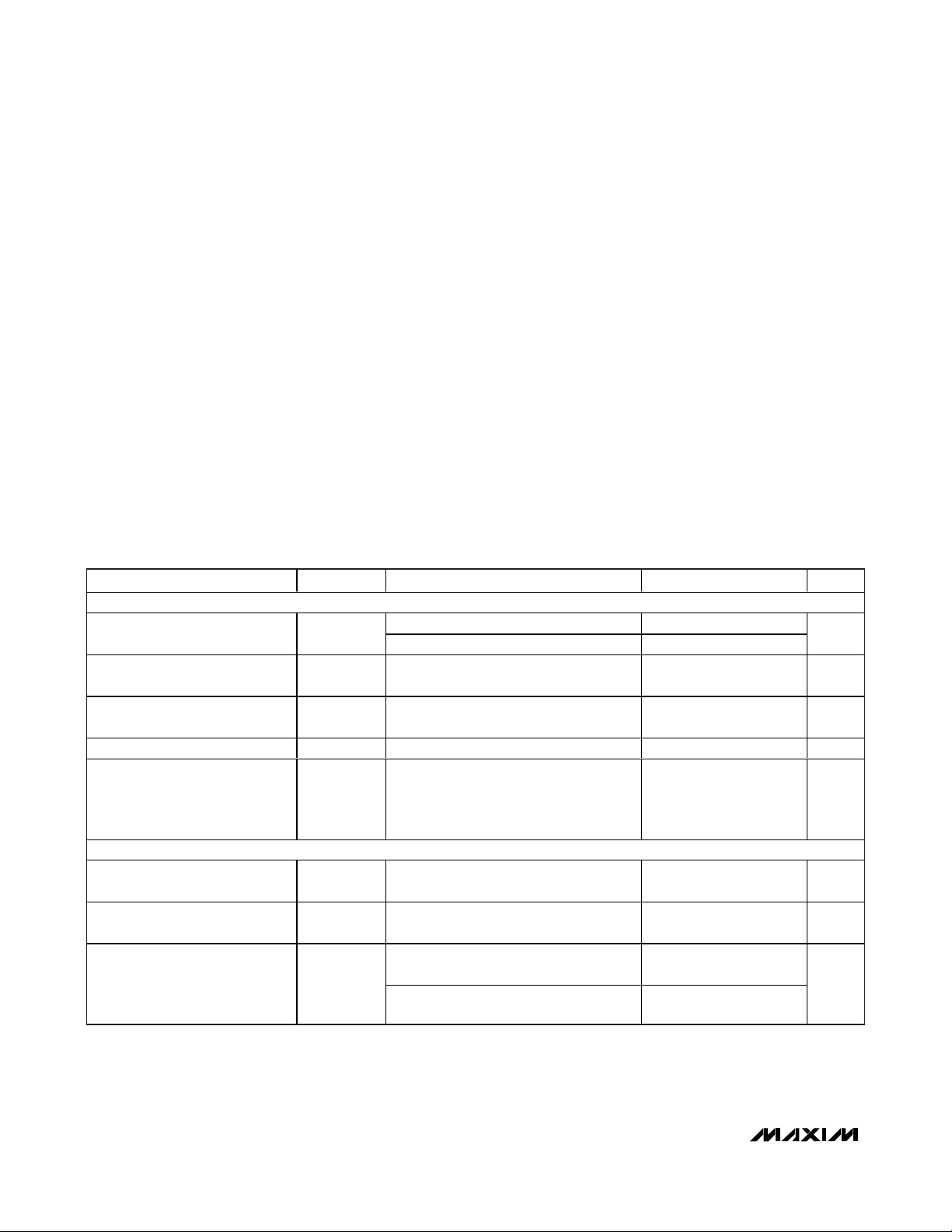
MAX8744A
MAX8745A
THIN QFN
5mm x 5mm
TOP VIEW
29
30
28
27
12
11
13
DRVA
SHDN
ON3
ON5
REF
14
ONA
DL3
IN
LDO5
LX3
PGND
DL5
12
+
CSL3
4567
2324 22 20 19 18
CSH3
FB3
PGOOD5
CSL5
CSH5
FB5
ILIM
PGOODA
3
21
31
10
FBA
SKIP
32
9
OUTA
FSEL
PGOOD3
26
15
BST5
BST3
25
16
DH5
GND
LX5
8
17
DH3
Pin Configuration
Ordering Information
Dual Mode is a trademark of Maxim Integrated Products, Inc.
EVALUATION KIT
AVAILABLE
PART TEMP RANGE
MAX8744AETJ+ -40°C to +85°C
MAX8745AETJ+* -40°C to +85°C
PINPACKAGE
32 Thin QFN
(5mm x 5mm)
32 Thin QFN
(5mm x 5mm)
PKG
CODE
T3255-4
T3255-4
Page 2
MAX8744A/MAX8745A
High-Efficiency, Quad Output, Main PowerSupply Controllers for Notebook Computers
2 _______________________________________________________________________________________
ABSOLUTE MAXIMUM RATINGS
Stresses beyond those listed under “Absolute Maximum Ratings” may cause permanent damage to the device. These are stress ratings only, and functional
operation of the device at these or any other conditions beyond those indicated in the operational sections of the specifications is not implied. Exposure to
absolute maximum rating conditions for extended periods may affect device reliability.
IN, SHDN, DRVA, OUTA to GND............................-0.3V to +28V
LDO5, ON3, ON5, ONA to GND ..............................-0.3V to +6V
PGOODA, PGOOD3, PGOOD5 to GND...................-0.3V to +6V
CSL3, CSH3, CSL5, CSH5 to GND ..........................-0.3V to +6V
REF, FB3, FB5, FBA to GND...................-0.3V to (V
LDO5
+ 0.3V)
SKIP, FSEL, ILIM to GND........................-0.3V to (V
LDO5
+ 0.3V)
DL3, DL5 to PGND..................................-0.3V to (V
LDO5
+ 0.3V)
BST3, BST5 to PGND .............................................-0.3V to +34V
BST3 to LX3..............................................................-0.3V to +6V
DH3 to LX3 ..............................................-0.3V to (V
BST3
+ 0.3V)
BST5 to LX5..............................................................-0.3V to +6V
DH5 to LX5 ..............................................-0.3V to (V
BST5
+ 0.3V)
GND to PGND .......................................................-0.3V to +0.3V
BST3, BST5 to LDO5 .............................................-0.3V to +0.3V
LDO Short Circuit to GND ..........................................Momentary
REF Short Circuit to GND ...........................................Momentary
DRVA Current (Sinking) ......................................................30mA
OUTA Shunt Current ...........................................................30mA
Continuous Power Dissipation (T
A
= +70°C)
Multilayer PCB
32-Pin, 5mm x 5mm TQFN
(derated 34.5mW/°C above +70°C) .........................2459mW
Operating Temperature Range ...........................-40°C to +85°C
Junction Temperature......................................................+150°C
Storage Temperature Range .............................-65°C to +150°C
Lead Temperature (soldering, 10s) ................................+300°C
ELECTRICAL CHARACTERISTICS
(Circuit of Figure 1, VIN= 12V, both SMPS enabled, FSEL = REF, SKIP = GND, ILIM = LDO5, FBA = LDO5, I
REF
= I
LDO5
= I
OUTA
=
no load, T
A
= 0°C to +85°C, unless otherwise noted. Typical values are at TA= +25°C.)
INPUT SUPPLIES (Note 1)
VIN Input Voltage Range V
VIN Operating Supply Current I
VIN Standby Supply Current I
VIN Shutdown Supply Current I
Quiescent Power Consumption P
MAIN SMPS CONTROLLERS
3.3V Output Voltage in Fixed
Mode
5V Output Voltage in Fixed Mode V
Feedback Voltage in Adjustable
Mode (Note 2)
PARAMETER SYMBOL CONDITIONS MIN TYP MAX UNITS
IN
IN
IN(STBY)
IN(SHDN)VIN
Q
V
OUT3
OUT5
V
FB_
LDO5 in regulation 5.4 26.0
IN = LDO5, V
LDO5 switched over to CSL5, either
SMPS on
VIN = 6V to 26V, both SMPS off, includes
I
SHDN
= 6V to 26V 8 20 µA
Both S M P S on, FB3 = FB5 = LD O5,
SKIP = GN D , V
= 15V ,
V
OU T A
P
+ P
IN
C S L 3
VIN = 6V to 26V, SKIP = FB3 = LDO5,
0 < V
CSH3
VIN = 6V to 26V, SKIP = FB5 = LDO5,
0 < V
CSH5
VIN = 6V to 26V, FB3 or FB5
duty factor = 20% to 80%
VIN = 6V to 26V, FB3 or FB5
duty factor = 50%
< 4.4V 4.5 5.5
CSL5
20 36 µA
65 120 µA
+ P
- V
- V
C S L 3
C S L 5
CSL3
CSL5
= 3.5V , V
+ P
OU T A
< 50mV (Note 2)
< 50mV (Note 2)
C S L 5
= 5.3V ,
3.5 4.5 mW
3.265 3.315 3.365 V
4.94 5.015 5.09 V
1.980 2.010 2.040
1.990 2.010 2.030
V
V
Page 3
MAX8744A/MAX8745A
High-Efficiency, Quad Output, Main Power-
Supply Controllers for Notebook Computers
_______________________________________________________________________________________ 3
ELECTRICAL CHARACTERISTICS (continued)
(Circuit of Figure 1, VIN= 12V, both SMPS enabled, FSEL = REF, SKIP = GND, ILIM = LDO5, FBA = LDO5, I
REF
= I
LDO5
= I
OUTA
=
no load, T
A
= 0°C to +85°C, unless otherwise noted. Typical values are at TA= +25°C.)
Idle Mode is a trademark of Maxim Integrated Products, Inc.
PARAMETER SYMBOL CONDITIONS MIN TYP MAX UNITS
Output Voltage Adjust Range Either SMPS 2.0 5.5 V
FB3, FB5 Dual Mode Threshold 3.0
Feedback Input Leakage Current V
DC Load Regulation
= V
FB3
= 2.1V -0.1 +0.1 µA
FB5
Either SMPS, SKIP = LDO5,
- V
0 < V
CSH_
CSL_
< 50mV
Line Regulation Error Either SMPS, 6V < VIN < 26V 0.03 %/V
FSEL = GND 170 200 230
Operating Frequency (Note 1) f
OSC
FSEL = REF 270 300 330
FSEL = LDO5 425 500 575
Maximum Duty Factor D
Minimum On-Time t
MAX
ONMIN
(Note 1) 97.5 99 %
SMPS3-to-SMPS5 Phase Shift SMPS5 starts after SMPS3
CURRENT LIMIT
ILIM Adjustment Range 0.5 V
Current-Sense Input Leakage
Current
Current-Limit Threshold (Fixed) V
Current-Limit Threshold
(Adjustable)
Current-Limit Threshold
(Negative)
Current-Limit Threshold
(Zero Crossing)
V
V
LIMIT
LIMIT
NEG
V
ZX
CSH3 = CSH5 = GND or LDO5 -1 +1 µA
V
V
V
V
CSH
CSH
CSH
CSH
_ - V
_ - V
_ - V
_ - V
_, ILIM = LDO5 45 50 55 mV
CSL
V
= 2.00V 185 200 215
_
CSL
_, SKIP = ILIM = LDO5 -67 -60 -53 mV
CSL
_, SKIP = LDO5, adjustable
CSL
ILIM
= 1.00V 94 100 106
V
ILIM
mode, percent of current limit
V
_ - V
CSH
ILIM = LDO5
_, SKIP = GND,
CSL
036mV
ILIM = LDO5 6 10 14 mV
Idle Mode™ Threshold V
IDLE
_ - V
CSH
SKIP = GND
CSL
_,
With respect to
current-limit
threshold (V
LIMIT
)
V
ILIM = LDO5 2.5 5 7.5 mV
Idle Mode Threshold
(Low Audible-Noise Mode)
V
IDLE
V
_ - V
CSH
SKIP = REF
CSL
_,
With respect to
current-limit
threshold (V
LIMIT
)
ILIM Leakage Current ILIM = GND or REF -1 +1 µA
V
LOO5
- 1.0
V
LOO5
- 0.4
-0.1 %
100 ns
40 %
144 Deg
REF
-120 %
20 %
10 %
V
kHz
V
mV
Page 4
MAX8744A/MAX8745A
High-Efficiency, Quad Output, Main PowerSupply Controllers for Notebook Computers
4 _______________________________________________________________________________________
ELECTRICAL CHARACTERISTICS (continued)
(Circuit of Figure 1, VIN= 12V, both SMPS enabled, FSEL = REF, SKIP = GND, ILIM = LDO5, FBA = LDO5, I
REF
= I
LDO5
= I
OUTA
=
no load, T
A
= 0°C to +85°C, unless otherwise noted. Typical values are at TA= +25°C.)
)
PARAMETER SYMBOL CONDITIONS MIN TYP MAX UNITS
Soft-Start Ramp Time t
Soft-Stop Ramp Time t
SSTART
SSTOP
Measured from the rising edge of ON_ to
full scale
Measured from the falling edge of ON_ to
full scale
INTERNAL FIXED LINEAR REGULATORS
LDO5 Output Voltage V
LDO5
ON5 = GND, 6V < VIN < 26V,
0 < I
LDO5
< 100mA
LDO5 Undervoltage-Lockout Fault Rising edge, hysteresis = 1%
Short-Circuit Current (Switched
Over to CSL5)
LDO5 = GND, V
> 4.7V 200 425 mA
CSL5
4.85 4.95 5.10 V
3.7 4.0 4.1 V
AUXILIARY LINEAR REGULATOR
DRVA Voltage Range V
DRVA Drive Current
FBA Regulation Threshold V
FBA Load Regulation V
DRVA
FBA
V
= 1.05V, V
FBA
= 0.965V, V
V
FBA
V
DRVA
DRA
= 5V, I
= 5V, I
= 5V 0.4
DRVA
= 5V 10
DRVA
= 1mA (sink) 0.98 1.00 1.02 V
DRVA
= 0.5mA to 5mA -1.2 -2.2 %
DRVA
0.5 26.0 V
OUTA Shunt Trip Level Rising edge 25 26 27 V
FBA Leakage Current V
Secondary Feedback Regulation
Threshold
= 1.035V -0.1 +0.1 µA
FBA
V
- V
DRVA
OUTA
DL5 Pulse Width
OUTA Leakage Current I
OUTA
V
DRVA
= V
= 25V 50 µA
OUTA
REFERENCE (REF)
Reference Voltage V
Reference Load-Regulation Error ΔV
REF Lockout Voltage V
REF(UVLO
REF
REF
LDO5 in regulation, I
I
= -5µA to +50µA -10 +10 mV
REF
= 0 1.985 2.00 2.015 V
REF
Rising edge 1.8 V
FAULT DETECTION
Output Overvoltage Trip Threshold
(MAX8744A Only)
Outp ut Over vol tag e Faul t
P r op ag ati on D elay (M AX 8744A Only)
t
OVP
With respect to error-comparator
threshold
81114%
50mV overdrive 10 µs
2ms
4ms
0V
1/
3f
OSC
mA
µs
Page 5

MAX8744A/MAX8745A
High-Efficiency, Quad Output, Main Power-
Supply Controllers for Notebook Computers
_______________________________________________________________________________________ 5
ELECTRICAL CHARACTERISTICS (continued)
(Circuit of Figure 1, VIN= 12V, both SMPS enabled, FSEL = REF, SKIP = GND, ILIM = LDO5, FBA = LDO5, I
REF
= I
LDO5
= I
OUTA
=
no load, T
A
= 0°C to +85°C, unless otherwise noted. Typical values are at TA= +25°C.)
)
Output Undervoltage Protection
Trip Threshold
Output Undevoltage Fault
Propagation Delay
Output Undervoltage Protection
Blanking Time
PGOOD_ Lower Trip Threshold
PGOOD_ Propagation Delay t
PGOOD_ Output Low Voltage I
PGOOD_ Leakage Current I
Thermal-Shutdown Threshold t
GATE DRIVERS
DH_ Gate-Driver On-Resistance R
DL_ Gate-Driver On-Resistance R
DH_ Gate-Driver Source/Sink
Current
DL_ Gate-Driver Source Current
DL_ Gate-Driver Sink Current I
Dead Time t
Internal BST_ Switch
On-Resistance
BST_ Leakage Current V
INPUTS AND OUTPUTS
SHDN Input Trip Level
ONA Logic Input Voltage Hysteresis = 600mV (typ)
ON3, ON5 Input Voltage
PARAMETER SYMBOL CONDITIONS MIN TYP MAX UNITS
With respect to error-comparator
threshold
t
UVP
t
BLANK
PGOOD
PGOOD
SHDN
DH
DL
I
DH
I
DL
DL (SINK
DEAD
R
BST
50mV overdrive 10 µs
From rising edge of ON_ with respect to
f
SW
With respect to error-comparator
threshold, hysteresis = 1% (typ)
Falling edge, 50mV overdrive 10
_
Rising edge, 50mV overdrive 1
= 1mA 0.4 V
SINK
_ High state, PGOOD_ forced to 5.5V 1 µA
Hysteresis = 15°C +160 °C
BST_ – LX_ forced to 5V 1.3 5 Ω
DL_, high state 1.7 5
DL_, low state 0.6 3
DH_ forced to 2.5V, BST_ – LX_ forced to
5V
DL_ forced to 2.5V 1.7 A
DL_ forced to 2.5V 3.3 A
DH_low to DL_high 15 45
DL_low to DH_high 15 44
I
= 10mA 5 Ω
BST
_ = 26V 2 20 µA
BST
Rising trip level 1.1 1.6 2.2
Falling trip level 0.96 1 1.04
High 2.4
Low 0.8
SMPS off level/clear fault level 0.8
Delay start level 1.9 2.1
SMPS on level 2.4
65 70 75 %
5000 6144 7000 1/f
-12 -10 -8 %
2A
OSC
µs
Ω
ns
V
V
V
Page 6
MAX8744A/MAX8745A
High-Efficiency, Quad Output, Main PowerSupply Controllers for Notebook Computers
6 _______________________________________________________________________________________
ELECTRICAL CHARACTERISTICS
(Circuit of Figure 1, VIN= 12V, both SMPS enabled, FSEL = REF, SKIP = GND, ILIM = LDO5, FBA = LDO5, I
REF
= I
LDO5
= I
OUTA
=
no load, T
A
= -40°C to +85°C, unless otherwise noted.) (Note 3)
ELECTRICAL CHARACTERISTICS (continued)
(Circuit of Figure 1, VIN= 12V, both SMPS enabled, FSEL = REF, SKIP = GND, ILIM = LDO5, FBA = LDO5, I
REF
= I
LDO5
= I
OUTA
=
no load, T
A
= 0°C to +85°C, unless otherwise noted. Typical values are at TA= +25°C.)
PARAMETER SYMBOL CONDITIONS MIN TYP MAX UNITS
V
LDO5
- 0.4
Tri-Level Input Logic SKIP, FSEL
High
REF 1.65 2.35
GND 0.5
Input Leakage Current
SKIP, FSEL forced to GND or LDO5 -1 +1
SHDN forced to GND or 26V -1 +1
INPUT SUPPLIES (Note 1)
VIN Input Voltage Range VIN
VIN Operating Supply Current I
VIN Standby Supply Current I
VIN Shutdown Supply Current I
Quiescent Power Consumption P
MAIN SMPS CONTROLLERS
3.3V Output Voltage in Fixed
Mode
5V Output Voltage in Fixed Mode V
Feedback Voltage in Adjustable
Mode
Output Voltage Adjust Range
FB3, FB5 Dual Mode Threshold
Operating Frequency (Note 1) f
Maximum Duty Factor D
PARAMETER SYMBOL CONDITIONS MIN MAX UNITS
LDO5 in regulat ion 5.4 26.0
IN = LDO5, V
LDO5 switched over to CSL5, either SMPS on 40 μA
IN
IN(STBY)
IN(SHDN) VIN
VIN = 6V to 26V, both SMPS off, includes
I
SHDN
= 6V to 26V 20 μA
< 4.4V 4.5 5.5
CSL5
Both SMPS on, FB3 = FB5 = LDO5; SKIP =
GND, V
Q
V
OUTA
P
+ P
IN
V
OUT3
OUT5
V
VIN = 6V to 26V, SKIP = FB3 = LDO5,
0 < V
VIN = 6V to 26V, SKIP = FB5 = LDO5,
0 < V
VIN = 6V to 26V, FB3 or FB5
FB_
duty factor = 20% to 80% (Note 2)
Either SMPS 2.0 5.5 V
3V
CSL3
= 15V,
CSL3
- V
CSH3
- V
CSH5
= 3.5V, V
+ P
+ P
CSL5
< 50mV (Note 2)
CSL3
< 50mV (Note 2)
CSL5
CSL5
= 5.3V,
OUTA
3.255 3.375 V
4.925 5.105 V
1.974 2.046 V
FSEL = GND 170 230
OSC
FSEL = REF 270 330
FSEL = LDO5 425 575
97 %
MAX
120 μA
4.5 mW
V
LDO5
0.4
-
µA
kHz
V
V
V
Page 7
MAX8744A/MAX8745A
High-Efficiency, Quad Output, Main Power-
Supply Controllers for Notebook Computers
_______________________________________________________________________________________ 7
ELECTRICAL CHARACTERISTICS (continued)
(Circuit of Figure 1, VIN= 12V, both SMPS enabled, FSEL = REF, SKIP = GND, ILIM = LDO5, FBA = LDO5, I
REF
= I
LDO5
= I
OUTA
=
no load, T
A
= -40°C to +85°C, unless otherwise noted.) (Note 3)
CURRENT LIMIT
ILIM Adjustment Range
Current-Limit Threshold (Fixed) V
Current-Limit Thresho ld
(Adjustable)
PARAMETER SYMBOL CONDITIONS MIN MAX UNITS
0.5 V
LIMIT VCSH
V
LIMIT VCSH
_ - V
_ - V
_, ILIM = LDO5 44 56 mV
CSL
V
= 2.00V 185 215
CSL
_
ILIM
= 1.00V 93 107
V
ILIM
INTERNAL FIXED LINEAR REGULATORS
LDO5 Output Voltage V
LDO5 Undervoltage-Lockout
Fault Threshold
LDO5 Bootstrap Switch
LDO5
ON5 = GND, 6V < VIN < 26V,
Risi ng edge, hysteresi s = 1% (typ) 3.7 4.1 V
Risi ng edge of CSL5, hysteres is = 1% (typ) 4.30 4.75 V
4.85 5.10 V
Short-Circuit Current LDO5 = GND, ON5 = GND 450 mA
Short-Circuit Current (Switched
over to CSL5)
AUXILIARY LINEAR REGULATOR
DRVA Voltage Range V
DRVA
DRVA Dri ve Current
FBA Regulation Threshold V
LDO5 = GND, V
0.5 26.0 V
V
= 1.05V, V
FBA
= 0.965V, V
V
FBA
V
FBA
DRVA
= 5V, I
> 4.7V 200 mA
CSL5
= 5V 0.4
DRVA
= 5V 10
DRVA
= 1mA (sink) 0.98 1.02 V
DRVA
OUTA Shunt Trip Level 25 27 V
REFERENCE (REF)
Reference Voltage V
LDO5 in regulation, I
REF
= 0 1.980 2.020 V
REF
V
REF
mV
mA
Page 8
MAX8744A/MAX8745A
High-Efficiency, Quad Output, Main PowerSupply Controllers for Notebook Computers
8 _______________________________________________________________________________________
ELECTRICAL CHARACTERISTICS (continued)
(Circuit of Figure 1, VIN= 12V, both SMPS enabled, FSEL = REF, SKIP = GND, ILIM = LDO5, FBA = LDO5, I
REF
= I
LDO5
= I
OUTA
=
no load, T
A
= -40°C to +85°C, unless otherwise noted.) (Note 3)
Note 1: The MAX8744A/MAX8745A cannot operate over all combinations of frequency, input voltage (VIN), and output voltage. For
large input-to-output differentials and high switching-frequency settings, the required on-time may be too short to maintain
the regulation specifications. Under these conditions, a lower operating frequency must be selected. The minimum on-time
must be greater than 150ns, regardless of the selected switching frequency. On-time and off-time specifications are measured from 50% point to 50% point at the DH_ pin with LX_ = GND, V
BST_
= 5V, and a 250pF capacitor connected from
DH_ to LX_. Actual in-circuit times may differ due to MOSFET switching speeds.
Note 2: When the inductor is in continuous conduction, the output voltage has a DC-regulation level lower than the error-comparator
threshold by 50% of the ripple. In discontinuous conduction (SKIP = GND, light load), the output voltage has a DC regulation level higher than the trip level by approximately 1.1% due to slope compensation.
Note 3: Specifications from -40°C to +85°C are guaranteed by design, not production tested.
FAULT DETECTION
Output Overvoltage Trip
Threshold (MAX8744A Only)
Output Undervoltage Protection
PGOOD_ Lower Trip Threshold
PGOOD_ Output Low Voltage I
GATE DRIVERS
DH_ Gate-Driver On-Resistance R
DL_ Gate-Driver On-Resistance R
INPUTS AND OUTPUTS
SHDN Input Trip Level
ONA Logic Input Voltage Hysteresis = 600mV
Tri-Level Input Logic SKIP, FSEL
PARAMETER SYMBOL CONDITIONS MIN TYP MAX UNITS
With respect to error comparator threshold 8 14 %
With respect to error comparator threshold 65 75 %
With respect to error comparator threshold,
hysteresis = 1%
= 1mA 0.4 V
SINK
BST_ – LX_ forced to 5V 5 Ω
DH
DL_, high state 5
DL
DL_, low state 3
Rising trip level 1.0 2.3
Falling trip level 0.96 1.04
High 2.4
Low 0.8
SMPS off level/clear fault level 0.8
Delay start level 1.9 2.1ON3, ON5 Input Voltage
SMPS on level 2.4
High V
REF 1.65 2.35
GND 0.5
-12 -8 %
LDO5
- 0.4
Ω
V
V
V
V
Page 9
MAX8744A/MAX8745A
High-Efficiency, Quad Output, Main Power-
Supply Controllers for Notebook Computers
_______________________________________________________________________________________
9
Typical Operating Characteristics
(Circuit of Figure 1, VIN= 12V, SKIP = GND, FSEL = REF, TA= +25°C, unless otherwise noted.)
5V OUTPUT EFFICIENCY
vs. LOAD CURRENT
100
90
80
70
EFFICIENCY (%)
60
50
0.001 0.01 0.1 1 10
7V
20V
LOAD CURRENT (A)
3.3V OUTPUT EFFICIENCY
vs. LOAD CURRENT
100
7V
90
80
12V
SKIP MODE
PWM MODE
12V
20V
MAX8744A toc01
MAX8744A toc04
100
90
80
70
EFFICIENCY (%)
60
50
100
90
80
5V OUTPUT EFFICIENCY
vs. LOAD CURRENT
SKIP MODE
LOW-NOISE
MODE
0.001 0.01 0.1 1 10
LOAD CURRENT (A)
PWM MODE
3.3V OUTPUT EFFICIENCY
vs. LOAD CURRENT
SKIP MODE
MAX8744A toc02
OUTPUT VOLTAGE (V)
MAX8744A toc05
5V OUTPUT VOLTAGE
vs. LOAD CURRENT
5.10
SKIP MODE
5.05
5.00
PWM MODE
4.95
4.90
0.0 1.0 2.0 3.0 4.0 5.0
LOW-NOISE MODE
LOAD CURRENT (A)
3.3V OUTPUT VOLTAGE
vs. LOAD CURRENT
3.39
SKIP MODE
3.36
LOW-NOISE MODE
3.33
MAX8744A toc03
MAX8744A toc06
70
EFFICIENCY (%)
60
50
0.001 0.01 0.1 1 10
LOAD CURRENT (A)
OUTPUT VOLTAGE DEVIATION
vs. INPUT VOLTAGE
3
2
1
0
-1
OUTPUT VOLTAGE DEVIATION (%)
-2
-3
0 4 8 12 16 20
3.3V OUTPUT
5.0V OUTPUT
INPUT VOLTAGE (V)
SKIP MODE
PWM MODE
70
EFFICIENCY (%)
60
50
100
MAX8744A toc07
10
SUPPLY CURRENT (mA)
1
LOW-NOISE
MODE
0.001 0.01 0.1 1 10
LOAD CURRENT (A)
PWM MODE
NO-LOAD INPUT SUPPLY CURRENT
vs. INPUT VOLTAGE
PWM MODE
LOW-NOISE MODE
SKIP MODE
0 4 8 12 16 20
INPUT VOLTAGE (V)
3.30
PWM MODE
OUTPUT VOLTAGE (V)
3.27
3.24
012345
LOAD CURRENT (A)
STANDBY AND SHUTDOWN INPUT CURRENT
vs. INPUT VOLTAGE
100
MAX8744A toc08
STANDBY (ONx = GND)
10
SUPPLY CURRENT (μA)
1
0 4 8 12 16 20
INPUT VOLTAGE (V)
SHUTDOWN
(SHDN = GND)
MAX8744A toc09
Page 10
MAX8744A/MAX8745A
High-Efficiency, Quad Output, Main PowerSupply Controllers for Notebook Computers
10 ______________________________________________________________________________________
Typical Operating Characteristics (continued)
(Circuit of Figure 1, VIN= 12V, SKIP = GND, FSEL = REF, TA= +25°C, unless otherwise noted.)
3.3V IDLE MODE CURRENT
vs. INPUT VOLTAGE
3
SKIP MODE
SKIP = GND
2
1
IDLE MODE CURRENT (A)
0
0 4 8 12 16 20
LOW-NOISE MODE
SKIP = REF
INPUT VOLTAGE (V)
1000
FORCED-PWM
MAX8744A toc10
100
LOW-NOISE SKIP
10
SWITCHING FREQUENCY (kHz)
1
0.001 10
LDO5 OUTPUT VOLTAGE
5.0
vs. LOAD CURRENT
4.9
4.8
4.7
OUTPUT VOLTAGE (V)
4.6
4.5
0 20406080100
LOAD CURRENT (mA)
12.2
MAX8744A toc13
12.1
12.0
OUTPUT VOLTAGE (V)
11.9
0 50 100 150
3.3V SWITCHING FREQUENCY
vs. LOAD CURRENT
PULSE SKIPPING
10.10.01
LOAD CURRENT (A)
OUTA OUTPUT VOLTAGE
vs. LOAD CURRENT
LOAD CURRENT (mA)
50
MAX8744A toc11
40
30
20
SAMPLE PERCENTAGE (%)
10
0
-10 -6 -2 2 6 10
12V
MAX8744A toc14
5V
2V
1V
5V
0
5V
0
REFERENCE OFFSET VOLTAGE
DISTRIBUTION
+85°C
+25°C
2V REF OFFSET VOLTAGE (mV)
SAMPLE SIZE = 125
LDO5 POWER-UP
1ms/div
A. INPUT SUPPLY, 5V/div
B. REF, 2V/div
SHDN = IN
C. LDO5, 5V/div
D. PGOOD5, 5V/div
MAX8744A toc12
MAX8744A toc15
A
B
C
D
Page 11
MAX8744A/MAX8745A
High-Efficiency, Quad Output, Main Power-
Supply Controllers for Notebook Computers
______________________________________________________________________________________
11
Typical Operating Characteristics (continued)
(Circuit of Figure 1, VIN= 12V, SKIP = GND, FSEL = REF, TA= +25°C, unless otherwise noted.)
SOFT-START WAVEFORM
MAX8744A toc16
B
A
400μs/div
C
D
E
3.3V
0
5V
0
0
0
12V
5A
0
A. ON3 AND ON5, 5V/div
B. 5V OUTPUT (V
OUT5
), 5V/div
C. PGOOD5, 5V/div
D. AUX LDO OUTPUT
(V
OUTA
), 10V/div
E. L5 INDUCTOR CURRENT,
5A/div
SMPS DELAYED STARTUP SEQUENCE
(ON3 = REF)
MAX8744A toc17
B
A
1ms/div
C
D
E
3.3V
0
5V
0
0
0
3.3V
0
A. ON5, 5V/div
B. 5V OUTPUT (V
OUT5
), 5V/div
C. PGOOD5, 5V/div
ON3 = REF
D. 3.3V OUTPUT (V
OUT3
),
5V/div
E. PGOOD3, 5V/div
SMPS DELAYED STARTUP SEQUENCE
(ON5 = REF)
MAX8744A toc18
B
A
1ms/div
C
D
E
3.3V
0
5V
0
0
0
3.3V
0
A. ON3, 5V/div
B. 5V OUTPUT (V
OUT5
), 5V/div
C. PGOOD5, 5V/div
ON5 = REF
D. 3.3V OUTPUT (V
OUT3
),
5V/div
E. PGOOD3, 5V/div
SMPS SHUTDOWN WAVEFORM
MAX8744A toc19
B
A
1ms/div
C
D
E
3.3V
5V
3.3V
5V
0
0
0
0
A. SHDN, 5V/div
B. 5V OUTPUT (V
OUT5
), 5V/div
C. PGOOD5, 5V/div
NO LOAD
D. 3.3V OUTPUT (V
OUT3
),
5V/div
E. PGOOD3, 5V/div
OUT5 LOAD TRANSIENT
MAX8744A toc20
B
A
20μs/div
C
D
5A
5.1V
1A
5A
12V
5.0V
4.9V
0
1A
A. I
OUT5
= 1A TO 5A, 5A/div
B. V
OUT5
, 50mV/div
C. INDUCTOR CURRENT,
5A/div
D. LX5, 10V/div
OUT3 LOAD TRANSIENT
MAX8744A toc21
B
A
20μs/div
C
D
3A
3.35V
1A
3A
12V
3.30V
3.25V
0
1A
A. I
OUT3
= 1A TO 3A, 5A/div
B. V
OUT3
, 50mV/div
C. INDUCTOR CURRENT,
5A/div
D. LX3, 10V/div
Page 12
MAX8744A/MAX8745A
High-Efficiency, Quad Output, Main PowerSupply Controllers for Notebook Computers
12 ______________________________________________________________________________________
Typical Operating Characteristics (continued)
(Circuit of Figure 1, VIN= 12V, SKIP = GND, FSEL = REF, TA= +25°C, unless otherwise noted.)
3.3V
0
3.35V
3.25V
2A
0
12V
0
SKIP TRANSITION
5V/div
A. SKIP,
B. 3.3V OUTPUT (V
100mV/div
0.5A LOAD
40μs/div
C. INDUCTOR CURRENT,
),
2A/div
OUT3
D. LX3, 10V/div
MAX8744A toc22
OUTPUT OVERVOLTAGE
FAULT PROTECTION (MAX8744A ONLY)
5V
A
0
3.3
B
0
5V
C
0
5V
D
0
1ms/div
A. PGOOD3, 5V/div
B. 3.3V OUTPUT (V
2V/div
OUT3
),
MAX8744A toc23
C. 5V OUTPUT (V
5V/div
D. DL3, 5V/div
OUT5
5V
A
0
3.3V
B
0
5V
C
0
12V
D
),
0
OUTPUT UNDERVOLTAGE
(SHORT-CIRCUIT) FAULT PROTECTION
20μs/div
A. LOAD FET GATE, 5V/div
B. 3.3V OUTPUT (V
30mΩ MOSFET
OUT3
), 1V/div
MAX8744A toc24
C. DL3, 5V/div
D. DH3, 10V/div
A
B
C
D
5.00V
4.95V
100mA
0
A. LDO5 OUTPUT, 50mV/div
B. LOAD CURRENT, 50mA/div
LDOH5 LOAD TRANSIENT
20μs/div
MAX8744A toc25
LDOHA LOAD TRANSIENT
5V
A
B
0
15.0V
14.5V
12.0V
11.9V
A. LOAD FET GATE, 5V/div
B. AUX LDO INPUT, 0.5V/div
0 TO 150mA LOAD TRANSIENT
20μs/div
MAX8744A toc26
C. AUX LDO OUTPUT (V
0.1V/div
A
B
C
),
OUTA
Page 13

MAX8744A/MAX8745A
High-Efficiency, Quad Output, Main Power-
Supply Controllers for Notebook Computers
______________________________________________________________________________________ 13
Pin Description
PIN NAME FUNCTION
1 ONA
2 DRVA
3 ILIM
4 SHDN
5 ON3
6 ON5
7 REF
8 GND Analog Ground. Connect the exposed backside pad to GND.
9 FSEL
Auxiliary LDO Enable Input. When ONA is pulled low, OUTA is high impedance and the secondary
feedback control is disabled. When ONA is driven high, the controller enables the auxiliary LDO.
Auxiliary LDO Transistor Base Driver. Connect DRVA to the base of a pnp power transistor. Add a
680Ω pullup resistor between the base and emitter.
Peak Current-Limit Threshold Adjustment. The current-limit threshold defaults to 50mV if ILIM is pulled
up to LDO5. In adjustable mode, the current-limit threshold across CSH_ and CSL_ is precisely 1/10
the voltage seen at ILIM over a 0.5V to 2.0V range. The logic threshold for switchover to the 50mV
default value is approximately V
Shutdown Control Input. The device enters its 8µA supply-current shutdown mode if V
than the SHDN input falling edge trip level and does not restart until V
input rising-edge trip level. Connect SHDN to V
through a resistive voltage-divider to implement a programmable undervoltage lockout.
V
IN
3.3V SMPS Enable Input. Driving ON3 high enables the 3.3V SMPS, while pulling ON3 low disables
the 3.3V SMPS. If ON3 is connected to REF, the 3.3V SMPS starts after the 5V SMPS reaches
regulation (delayed start). Drive ON3 below the clear fault level to reset the fault latch.
5V SMPS Enable Input. Driving ON5 high enables the 5V SMPS, while pulling ON5 low disables the
5V SMPS. If ON5 is connected to REF, the 5V SMPS starts after the 3.3V SMPS reaches regulation
(delayed start). Drive ON5 below the clear fault level to reset the fault latch.
2.0V Reference Voltage Output. Bypass REF to analog ground with a 0.1µF or greater ceramic
capacitor. The reference sources up to 50µA for external loads. Loading REF degrades outputvoltage accuracy according to the REF load-regulation error. The reference shuts down when the
system pulls SHDN low.
Frequency Select Input. This three-level logic input sets the controllers’ switching frequency. Connect
to LDO5, REF, or GND to select the following typical switching frequencies:
LDO5 = 500kHz, REF = 300kHz, GND = 200kHz.
LDO5
- 1V.
for automatic startup. SHDN can be connected to
IN
is less
is greater than the SHDN
SHDN
SHDN
10 SKIP
11 FB5
12 CSH5
13 CSL5
14 PGOOD5
Pulse-Skipping Control Input. Connect to LDO5 for low-noise, forced-PWM operation. Connect to REF
for automatic, low-noise, pulse-skipping operation at light loads. Connect to GND for automatic, highefficiency, pulse-skipping operation at light loads.
Feedback Input for the 5V SMPS. Connect to LDO5 for the preset 5V output. In adjustable mode, FB5
regulates to 2V.
P osi ti ve C ur r ent- S ense Inp ut for the 5V S M P S . C onnect to the p osi ti ve ter m i nal of the cur r ent- sense
el em ent. Fi g ur e 7 d escr i b es tw o d i ffer ent cur r ent- sensi ng op ti ons— usi ng accur ate sense r esi stor s or
l ossl ess i nd uctor D C R sensi ng .
Output-Sense and Negative Current-Sense Input for the 5V SMPS. When using the internal preset 5V
feedback-divider (FB5 = LDO5), the controller uses CSL5 to sense the output voltage. Connect to the
negative terminal of the current-sense element. CSL5 also serves as the bootstrap input for LDO5.
Open-Drain, Power-Good Output for the 5V SMPS. PGOOD5 is pulled low if CSL5 drops more than
10% (typ) below the normal regulation point. PGOOD5 is held low during soft-start and shutdown.
PGOOD5 becomes high impedance when CSL5 is in regulation.
Page 14

MAX8744A/MAX8745A
High-Efficiency, Quad Output, Main PowerSupply Controllers for Notebook Computers
14 ______________________________________________________________________________________
Pin Description (continued)
PIN NAME FUNCTION
Boost Flying Capacitor Connection for the 5V SMPS. The MAX8744A/MAX8745A include an internal
15 BST5
16 DH5 High-Side Gate-Driver Output for the 5V SMPS. DH5 swings from LX5 to BST5.
17 LX5
18 DL5 Low-Side Gate-Driver Output for the 5V SMPS. DL5 swings from PGND to LDO5.
19 PGND Power Ground
20 LDO5
21 IN
22 PGOODA
23 DL3 Low-Side Gate-Driver Output for the 3.3V SMPS. DL3 swings from PGND to LDO5.
24 LX3
25 DH3 High-Side Gate-Driver Output for the 3.3V SMPS. DH3 swings from LX3 to BST3.
26 BST3
boost switch connected between LDO5 and BST5. Connect to an external capacitor as shown in
Figure 1.
Inductor Connection for the 5V SMPS. Connect LX5 to the switched side of the inductor. LX5 serves
as the lower supply rail for the DH5 high-side gate driver.
5V Internal Linear-Regulator Output. Bypass with 4.7µF minimum (1µF/25mA). Provides at least
100mA for the DL_ low-side gate drivers, the DH_ high-side drivers through the BST switches, the
PWM controller, logic, reference, and external loads. If CSL5 is greater than 4.5V and soft-start is
complete, the linear regulator shuts down, and LDO5 connects to CSL5 through a 1Ω switch rated for
loads up to 200mA.
Input of the Startup Circuitry and the LDO5 Internal 5V Linear Regulator. Bypass to PGND with a
0.22µF or greater ceramic capacitor close to the IC.
Open-Drain, Power-Good Output for the Auxiliary LDO. PGOODA is pulled low if FBA drops more
than 10% (typ) below the normal regulation point, and when the auxiliary LDO is shut down. PGOODA
becomes high impedance when FBA is in regulation.
Inductor Connection for the 3.3V SMPS. Connect LX3 to the switched side of the inductor. LX3 serves
as the lower supply rail for the DH3 high-side gate driver.
Boost Flying Capacitor Connection for the 3.3V SMPS. The MAX8744A/MAX8745A include an internal
boost switch connected between LDO5 and BST3. Connect to an external capacitor as shown in
Figure 1.
Open-Drain, Power-Good Output for the 3.3V SMPS. PGOOD3 is pulled low if CSL3 drops more than
27 PGOOD3
28 CSL3
29 CSH3
30 FB3
31 FBA
10% (typ) below the normal regulation point. PGOOD3 is held low during soft-start and shutdown.
PGOOD3 becomes high impedance when CSL3 is in regulation.
Output Sense and Negative Current Sense for the 3.3V SMPS. When using the internal preset 3.3V
feedback divider (FB3 = LDO5), the controller uses CSL3 to sense the output voltage. Connect to the
negative terminal of the current-sense element.
Positive Current-Sense Input for the 3.3V SMPS. Connect to the positive terminal of the current-sense
element. Figure 7 describes two different current-sensing options—using accurate sense resistors or
lossless inductor DCR sensing.
Feedback Input for the 3.3V SMPS. Connect to LDO5 for fixed 3.3V output. In adjustable mode, FB3
regulates to 2V.
Auxiliary LDO Feedback Input. Connect a resistive voltage-divider from OUTA to analog ground to
adjust the auxiliary linear-regulator output voltage. FBA regulates at 1V.
Page 15

MAX8744A/MAX8745A
High-Efficiency, Quad Output, Main Power-
Supply Controllers for Notebook Computers
______________________________________________________________________________________ 15
Pin Description (continued)
Table 1. Component Selection for Standard Applications
Pin Description (continued)
PIN NAME FUNCTION
PIN NAME FUNCTION
Adjustable Auxiliary Linear-Regulator Output. Bypass OUTA to GND with 1µF or greater capacitor
Boost Flying Capacitor Connection for the 5V SMPS. The MAX8744A/MAX8745A include an internal
(1µF/25mA). When DRVA < OUTA, the secondary feedback control triggers the DL5 for 1µs forcing
15 BST5
32 OUTA
16 DH5 High-Side Gate-Driver Output for the 5V SMPS. DH5 swings from LX5 to BST5.
17 LX5
EP EP Exposed Pad. Connect the exposed backside pad to analog ground.
18 DL5 Low-Side Gate-Driver Output for the 5V SMPS. DL5 swings from PGND to LDO5.
19 PGND Power Ground
20 LDO5
COMPONENT
INPUT VOLTAGE VIN = 7V TO 24V VIN = 7V TO 24V
21 IN
C
, Input Capacitor
IN_
5V OUTPUT
22 PGOODA
C
, Output Capacitor
OUT5
23 DL3 Low-Side Gate-Driver Output for the 3.3V SMPS. DL3 swings from PGND to LDO5.
L5/T5 Inductor/Transformer
24 LX3
25 DH3 High-Side Gate-Driver Output for the 3.3V SMPS. DH3 swings from LX3 to BST3.
NH5 High-Side MOSFET
26 BST3
27 PGOOD3
NL5 Low-Side MOSFET
3V OUTPUT
28 CSL3
, Output Capacitor
C
OUT3
29 CSH3
L3, Inductor
30 FB3
NH3 High-Side MOSFET
31 FBA
boost switch connected between LDO5 and BST5. Connect to an external capacitor as shown in
the controller to recharge the auxiliary storage capacitor. When DRVA exceeds 25V, the
Figure 1.
MAX8744A/MAX8745A enable a 10mA shunt on OUTA, preventing the storage capacitor from rising
to unsafe levels due to the transformer’s leakage inductance. Pulling ONA high enables the linear-
Inductor Connection for the 5V SMPS. Connect LX5 to the switched side of the inductor. LX5 serves
regulator driver and the secondary feedback control.
as the lower supply rail for the DH5 high-side gate driver.
5V Internal Linear-Regulator Output. Bypass with 4.7µF minimum (1µF/25mA). Provides at least
100mA for the DL_ low-side gate drivers, the DH_ high-side drivers through the BST switches, the
PWM controller, logic, reference, and external loads. If CSL5 is greater than 4.5V and soft-start is
complete, the linear regulator shuts down, and LDO5 connects to CSL5 through a 1Ω switch rated for
loads up to 200mA.
Input of the Startup Circuitry and the LDO5 Internal 5V Linear Regulator. Bypass to PGND with a
(3) 10µF, 25V
0.22µF or greater ceramic capacitor close to the IC.
Taiyo Yuden TMK432BJ106KM
Open-Drain, Power-Good Output for the Auxiliary LDO. PGOODA is pulled low if FBA drops more
than 10% (typ) below the normal regulation point, and when the auxiliary LDO is shut down. PGOODA
2x 100µF, 6V, 35mΩ
becomes high impedance when FBA is in regulation.
SANYO 6TPE100MAZB
6.8µH, 6.4A, 18mΩ (max) 1:2
Inductor Connection for the 3.3V SMPS. Connect LX3 to the switched side of the inductor. LX3 serves
Sumida 4749-T132
as the lower supply rail for the DH3 high-side gate driver.
Fairchild Semiconductor
FDS6612A
Boost Flying Capacitor Connection for the 3.3V SMPS. The MAX8744A/MAX8745A include an internal
International Rectifier
boost switch connected between LDO5 and BST3. Connect to an external capacitor as shown in
IRF7807V
Figure 1.
Fairchild Semiconductor
Open-Drain, Power-Good Output for the 3.3V SMPS. PGOOD3 is pulled low if CSL3 drops more than
FDS6670S
10% (typ) below the normal regulation point. PGOOD3 is held low during soft-start and shutdown.
International Rectifier
PGOOD3 becomes high impedance when CSL3 is in regulation.
IRF7807VD1
Output Sense and Negative Current Sense for the 3.3V SMPS. When using the internal preset 3.3V
feedback divider (FB3 = LDO5), the controller uses CSL3 to sense the output voltage. Connect to the
2x 150µF, 4V, 35mΩ
negative terminal of the current-sense element.
SANYO 4TPE150MAZB
Positive Current-Sense Input for the 3.3V SMPS. Connect to the positive terminal of the current-sense
5.8µH, 8.6A, 16.2mΩ
element. Figure 7 describes two different current-sensing options—using accurate sense resistors or
Sumida
lossless inductor DCR sensing.
CDRH127/LD-5R8NC
Feedback Input for the 3.3V SMPS. Connect to LDO5 for fixed 3.3V output. In adjustable mode, FB3
Fairchild Semiconductor
regulates to 2V.
FDS6612A
Auxiliary LDO Feedback Input. Connect a resistive voltage-divider from OUTA to analog ground to
International Rectifier
adjust the auxiliary linear-regulator output voltage. FBA regulates at 1V.
IRF7807V
300kHz
5V AT 5A
3.3V AT 5A
(3) 10µF, 25V
Taiyo Yuden TMK432BJ106KM
2x 100µF, 6V, 35mΩ
SANYO 6TPE100MAZB
—
Fairchild Semiconductor
FDS6612A
International Rectifier
IRF7807V
Fairchild Semiconductor
FDS6670S
International Rectifier
IRF7807VD1
2x 100µF, 6V, 35mΩ
SANYO 6TPE100MAZB
3.9µH, 6.5A, 15mΩ
Sumida CDRH124-3R9NC
Fairchild Semiconductor
FDS6612A
International Rectifier
IRF7807V
500kHz
5V AT 3A
3.3V AT 5A
NL3 Low-Side MOSFET
Fairchild Semiconductor
FDS6670S
International Rectifier
IRF7807VD1
Fairchild Semiconductor
FDS6670S
International Rectifier
IRF7807VD1
Page 16

MAX8744A/MAX8745A
High-Efficiency, Quad Output, Main PowerSupply Controllers for Notebook Computers
16 ______________________________________________________________________________________
Figure 1. Standard Application Circuit
)
INPUT (V
C
IN
21
IN
C
IN
IN
N
H1
25
DH3
26
N
L1
C
REF
0.22μF
24
23
29
28
9
7
2
32
31
4
5
6
1
BST3
LX3
DL3
CSH3
CSL3
FSEL
REF
MAX8744A
MAX8745A
DRVA
OUTA
FBA
SHDN
ON3
ON5
ONA
C
3.3V PWM
OUTPUT
C
OUT3
L3
6.96kΩ
R2
3.48kΩ
C1
0.22μF
1000pF
R1
C3
SECONDARY
OUTPUT
12V LDO
OUTPUT
C
LDOA
4.7μF
BST1
0.1μF
D
L1
REF
(300kHz)
R10
680Ω
R5
110kΩ
R6
10kΩ
OFFON
DH5
BST5
LX5
DL5
PGND
GND
CSH5
CSL5
ILIM
FB5
FB3
LDO5
SKIP
PGOODA
PGOOD3
PGOOD5
T5
R3
10.5kΩ
R4
4.02kΩ
C2
0.22μF
C4
1000pF
R9
100kΩ
D1
CONNECT
TO 5V OR 3.3V
N
H2
16
15
C
BST2
0.1μF
17
18
N
L2
19
8
12
13
3
11
30
20
10
R7
100kΩ
22
27
14
C
LDO5
4.7μF
D
L2
5V LDO OUTPUT
R8
100kΩ
SECONDARY
OUTPUT
C
AUX
4.7μF
5V PWM
OUTPUT
C
OUT5
POWER-GOOD
POWER GROUND
ANALOG GROUND
SEE TABLE 1 FOR COMPONENT SPECIFICATIONS.
Page 17

MAX8744A/MAX8745A
High-Efficiency, Quad Output, Main Power-
Supply Controllers for Notebook Computers
______________________________________________________________________________________ 17
Detailed Description
The MAX8744A/MAX8745A standard application circuit
(Figure 1) generates the 5V/5A and 3.3V/5A typical of the
main supplies in a notebook computer. The input supply
range is 7V to 24V. See Table 1 for component selections, while Table 2 lists the component manufacturers.
The MAX8744A/MAX8745A contain two interleaved,
fixed-frequency, step-down controllers designed for lowvoltage power supplies. The optimal interleaved architecture guarantees out-of-phase operation, reducing the
input capacitor ripple. One internal LDO generates the
keep-alive 5V power. The MAX8744A/MAX8745A have
an auxiliary LDO with an adjustable output for generating either the 3.3V keep-alive supply or regulating the
low-power 12V system supply.
Fixed 5V Linear Regulator (LDO5)
An internal linear regulator produces a preset 5V lowcurrent output. LDO5 powers the gate drivers for the
external MOSFETs, and provides the bias supply
required for the SMPS analog controller, reference, and
logic blocks. LDO5 supplies at least 100mA for external and internal loads, including the MOSFET gate
drive, which typically varies from 5mA to 50mA,
depending on the switching frequency and external
MOSFETs selected. Bypass LDO5 with a 4.7µF or
greater ceramic capacitor (1µF per 25mA of load) to
guarantee stability under the full-load conditions.
The MAX8744A/MAX8745A switch-mode power supplies
(SMPS) require a 5V bias supply in addition to the highpower input supply (battery or AC adapter). This 5V bias
supply is generated by the controller’s internal 5V linear
regulator (LDO5). This bootstrapped LDO allows the
controller to power up independently. The gate-driver
input supply is connected to the fixed 5V linear-regulator
output (LDO5). Therefore, the 5V LDO supply must provide LDO5 (PWM controller) and the gate-drive power,
so the maximum supply current required is:
I
BIAS
= ICC+ fSW(Q
G(LOW)
+ Q
G(HIGH)
)
= 5mA to 50mA (typ)
where ICCis 0.7mA (typ), fSWis the switching frequency,
and Q
G(LOW)
and Q
G(HIGH)
are the MOSFET data
sheet’s total gate-charge specification limits at VGS= 5V.
SMPS to LDO Bootstrap Switchover
When the 5V main output voltage is above the LDO5
bootstrap-switchover threshold and has completed
soft-start, an internal 1Ω (typ) p-channel MOSFET
shorts CSL5 to LDO5, while simultaneously shutting
down the LDO5 linear regulator. This bootstraps the
device, powering the internal circuitry and external
loads from the 5V SMPS output (CSL5), rather than
through the linear regulator from the battery. Bootstrapping reduces power dissipation due to gate
charge and quiescent losses by providing power from
a 90%-efficient switch-mode source, rather than from a
much-less-efficient linear regulator. The current capability increases from 100mA to 200mA when the LDO5
output is switched over to CSL5. When ON5 is pulled
low, the controller immediately disables the bootstrap
switch and reenables the 5V LDO.
Reference (REF)
The 2V reference is accurate to ±1% over temperature
and load, making REF useful as a precision system reference. Bypass REF to GND with a 0.1µF or greater
ceramic capacitor. The reference sources up to 50µA
and sinks 5µA to support external loads. If highly accurate specifications are required for the main SMPS output voltages, the reference should not be loaded.
Loading the reference reduces the LDO5, CSL5
(OUT5), CSL3 (OUT3), and OUTA output voltages
slightly because of the reference load-regulation error.
System Enable/Shutdown (
SHDN
)
Drive SHDN below the precise SHDN input falling-edge
trip level to place the MAX8744A/MAX8745A in its lowpower shutdown state. The controller consumes only
8µA of quiescent current while in shutdown mode.
When shutdown mode activates, the reference turns off
after the controller completes the shutdown sequence
Table 2. Component Suppliers
SUPPLIER WEBSITE
AVX www.avx.com
Central Semiconductor www.centralsemi.com
Fairchild
International Rectifier www.irf.com
KEMET www.kemet.com
NEC/Tokin www.nec-tokin.com
Panasonic www.panasonic.com/industrial
Philips www.philips.com
Pulse www.pulseeng.com
Renesas www.renesas.com
SANYO www.edc.sanyo.com
Sumida www.sumida.com
Taiyo Yuden www.t-yuden.com
TDK www.component.tdk.com
TOKO www.tokoam.com
Vishay (Dale, Siliconix) www.vishay.com
www.fairchildsemi.com
Page 18

MAX8744A/MAX8745A
High-Efficiency, Quad Output, Main PowerSupply Controllers for Notebook Computers
18 ______________________________________________________________________________________
making the threshold to exit shutdown less accurate. To
guarantee startup, drive SHDN above 2V (SHDN input
rising-edge trip level). For automatic shutdown and
startup, connect SHDN to VIN. The accurate 1V fallingedge threshold on SHDN can be used to detect a specific input voltage level and shut the device down. Once
in shutdown, the 1.6V rising-edge threshold activates,
providing sufficient hysteresis for most applications.
SMPS POR, UVLO, and Soft-Start
Power-on reset (POR) occurs when LDO5 rises above
approximately 1V, resetting the undervoltage, overvoltage, and thermal-shutdown fault latches. The POR circuit also ensures that the low-side drivers are pulled
high until the SMPS controllers are activated. Figure 2 is
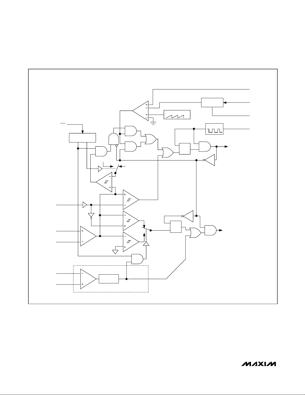
the MAX8744A/MAX8745A block diagram.
Figure 2. Block Diagram
FSEL
ILIM
SKIP
CSH3
CSL3
BST3
DH3
LX3
DL3
PGND
FB3
ON3
PGOOD5
PGOOD3
PGOODA
OSC
LDO5
LDO5
CONTROLLER
FB
DECODE
(FIGURE 5)
PWM3
(FIGURE 3)
INTERNAL
FB
POWER-GOOD AND FAULT
PROTECTION
(FIGURE 6)
MAX8744A
MAX8745A
IN
FAULT
5V LINEAR
REGULATOR
LDO BYPASS
CIRCUITRY
PWM5
CONTROLLER
(FIGURE 3)
DECODE
(FIGURE 5)
SECONDARY
FEEDBACK
LINEAR REGULATOR
LDO5
FB
2.0V
R
AUXILIARY
REF
R
SHDN
LDO5
CSH5
CSL5
BST5
DH5
LX5
DL5
ON5
FB5
REF
GND
DRVA
OUTA
FBA
ONA
Page 19

MAX8744A/MAX8745A
High-Efficiency, Quad Output, Main Power-
Supply Controllers for Notebook Computers
______________________________________________________________________________________ 19
The LDO5 input undervoltage-lockout (UVLO) circuitry
inhibits switching if the 5V bias supply (LDO5) is below
its 4V UVLO threshold. Once the 5V bias supply
(LDO5) rises above this input UVLO threshold and the
SMPS controllers are enabled (ON_ driven high), the
SMPS controllers start switching, and the output voltages begin to ramp up using soft-start. If the LDO5
voltage drops below the UVLO threshold, the controller
stops switching and pulls the low-side gate drivers low
until the LDO5 voltage recovers or drops below the
POR threshold.
The internal soft-start gradually increases the feedback
voltage with a 1V/ms slew rate. Therefore, the outputs
reach their nominal regulation voltage 2ms after the
SMPS controllers are enabled (see the SMPS Shutdown
Waveform in the
Typical Operating Characteristics
).
This gradual slew rate effectively reduces the input
surge current by minimizing the current required to
charge the output capacitors (I
OUT
= I
LOAD
+ C
OUT
x
V
OUT(NOM)
/ t
SLEW
).
SMPS Enable Controls (ON3, ON5)
ON3 and ON5 control SMPS power-up sequencing.
ON3 or ON5 rising above 2.4V enables the respective
outputs. ON3 or ON5 falling below 1.6V disables the
respective outputs. Driving ON_ below 0.8V clears the
overvoltage, undervoltage, and thermal fault latches.
SMPS Power-Up Sequencing
Connecting ON3 or ON5 to REF forces the respective
outputs off while the other output is below regulation
and starts after that output regulates. The second
SMPS remains on until the first SMPS turns off, the
device shuts down, a fault occurs, or LDO5 goes into
UVLO. Both supplies begin their power-down
sequence immediately when the first supply turns off.
Output Discharge (Soft-Shutdown)
When the switching regulators are disabled—when ON_
or SHDN is pulled low, or when an output undervoltage
fault occurs—the internal soft-shutdown gradually
decreases the feedback voltage with a 0.5V/ms slew rate.
Therefore, the regulation voltage drops to 0V within 4ms
after the SMPS controllers are disabled (see the SMPS
Shutdown Waveform in the
Typical Operating
Characteristics
). This slowly discharges the output
capacitance, eliminating the negative output voltages
caused by quickly discharging the output through the
inductor and low-side MOSFET. When an SMPS target
voltage discharges to 0.1V, its low-side driver (DL_) is
forced high, clamping the respective SMPS output to
GND. The reference remains active to provide an accurate threshold and to provide overvoltage protection. Both
SMPS controllers contain separate soft-shutdown circuits.
Table 3. Operating Mode Truth Table
*
SHDN is an accurate, low-voltage logic input with 1V falling-edge threshold voltage and 1.6V rising-edge threshold voltage. ON3
and ON5 are tri-level CMOS logic inputs, a logic-low voltage is less than 0.8V, a logic-high voltage is greater than 2.4V, and the middle-logic level is between 1.7V and 2.3V (see the
Electrical Characteristics
table).
MODE
Shutdown Mode Low X X OFF OFF OFF
Standby Mode High Low Low ON OFF OFF
Normal Operation High High High ON ON ON
3.3V SMPS Active High Low High ON OFF ON
5V SMPS Active High High Low
Normal Operation
(Delayed 5V SMPS
Startup)
Normal Operation
(Delayed 3.3V SMPS
Startup)
SHDN ON5 ON3 LDO5 5V SMPS 3V SMPS
High Ref High
High High Ref
INPUTS* OUTPUTS
OFF
LDO5 to CSL5 bypass
switch enabled
OFF
LDO5 to CSL5 bypass
switch enabled
OFF
LDO5 to CSL5 bypass
switch enabled
ON OFF
ON
Power-up after 3.3V
SMPS is in regulation
ON
ON
ON
Power-up after 5V
SMPS is in regulation
Page 20
MAX8744A/MAX8745A
High-Efficiency, Quad Output, Main PowerSupply Controllers for Notebook Computers
20 ______________________________________________________________________________________
Fixed-Frequency, Current-Mode
PWM Controller
The heart of each current-mode PWM controller is a
multi-input, open-loop comparator that sums two signals: the output-voltage error signal with respect to the
reference voltage and the slope-compensation ramp
(Figure 3). The MAX8744A/MAX8745A use a directsumming configuration, approaching ideal cycle-tocycle control over the output voltage without a
traditional error amplifier and the phase shift associated
with it.
Figure 3. PWM Controller Functional Diagram
FROM FB
(SEE FIGURE 5)
SKIP
TRI-LEVEL
DECODE
0.2 x V
LIMIT
0.1 x V
LIMIT
IDLE MODE
ILIM
CSH_
CSL_
A = 1/10
A = 1.2
CURRENT
PEAK CURRENT
LIMIT
NEG CURRENT
LIMIT
ZERO
CROSSING
AGND
SLOPE COMP
S
Q
R
SOFT-
START/STOP
OSC
R
Q
S
DH DRIVER
DL DRIVER
REF
ON_
FSEL
PGND
DRVA
OUTA
ONE-SHOT
5V SMPS ONLY
Page 21

MAX8744A/MAX8745A
High-Efficiency, Quad Output, Main Power-
Supply Controllers for Notebook Computers
_______________________________________
Frequency Selection (FSEL)
The FSEL input selects the PWM mode switching frequency. Table 4 shows the switching frequency based
on FSEL connection. High-frequency (500kHz) operation
optimizes the application for the smallest component
size, trading off efficiency due to higher switching losses.
This may be acceptable in ultraportable devices where
the load currents are lower. Low-frequency (200kHz)
operation offers the best overall efficiency at the expense
of component size and board space.
Forced-PWM Mode
The low-noise forced-PWM mode (SKIP = LDO5) disables the zero-crossing comparator, which controls the
low-side switch on-time. This forces the low-side gatedrive waveform to be constantly the complement of the
high-side gate-drive waveform, so the inductor current
reverses at light loads while DH_ maintains a duty factor
of V
OUT/VIN
. The benefit of forced-PWM mode is to keep
the switching frequency fairly constant. However, forcedPWM operation comes at a cost: the no-load 5V supply
current remains between 20mA to 50mA, depending on
the external MOSFETs and switching frequency.
Forced-PWM mode is most useful for avoiding audiofrequency noise and improving load-transient
response. Since forced-PWM operation disables the
zero-crossing comparator, the inductor current reverses under light loads.
Light-Load Operation Control (
SKIP
)
The MAX8744A/MAX8745A include a light-load operating mode control input (SKIP) used to enable or disable the zero-crossing comparator for both switching
regulators. When the zero-crossing comparator is
enabled, the regulator forces DL_ low when the current-sense inputs detect zero inductor current. This
keeps the inductor from discharging the output capacitors and forces the regulator to skip pulses under lightload conditions to avoid overcharging the output. When
the zero-crossing comparator is disabled, the regulator
is forced to maintain PWM operation under light-load
conditions (forced PWM).
Idle Mode Current-Sense Threshold
When pulse-skipping mode is enabled, the on-time of the
step-down controller terminates when the output voltage
exceeds the feedback threshold and when the current-
sense voltage exceeds the idle mode current-sense
threshold. Under light-load conditions, the on-time duration depends solely on the idle mode current-sense
threshold, which is 20% (SKIP = GND) of the full-load
current-limit threshold set by ILIM, or the low-noise current-sense threshold, which is 10% (SKIP = REF) of the
full-load current-limit threshold set by ILIM. This forces
the controller to source a minimum amount of power with
each cycle. To avoid overcharging the output, another
on-time cannot begin until the output voltage drops
below the feedback threshold. Since the zero-crossing
comparator prevents the switching regulator from sinking
current, the controller must skip pulses. Therefore, the
controller regulates the valley of the output ripple under
light-load conditions.
Automatic Pulse-Skipping Crossover
In skip mode, an inherent automatic switchover to PFM
takes place at light loads (Figure 4). This switchover is
affected by a comparator that truncates the low-side
switch on-time at the inductor current’s zero crossing.
The zero-crossing comparator senses the inductor current across CSH_ to CSL_. Once V
CSH
_ - V
CSL
_ drops
below the 3mV zero-crossing, current-sense threshold,
the comparator forces DL_ low (Figure 3). This mechanism causes the threshold between pulse-skipping
PFM and nonskipping PWM operation to coincide with
the boundary between continuous and discontinuous
inductor-current operation (also known as the “critical
conduction” point). The load-current level at which
PFM/PWM crossover occurs, I
LOAD(SKIP)
, is given by:
Table 4. FSEL Configuration Table
Figure 4. Pulse-Skipping/Discontinuous Crossover Point
FSEL SWITCHING FREQUENCY (kHz)
LDO5 500
REF 300
GND 200
VV V
I
LOAD SKIP
()
()
=
−
IN OUT OUT
Vf L
2
IN OSC
V
t
ON(SKIP)
INDUCTOR CURRENT
0
ON-TIME
OUT
=
VINf
OSC
TIME
I
PK
I
LOAD
= IPK / 2
Page 22

MAX8744A/MAX8745A
High-Efficiency, Quad Output, Main PowerSupply Controllers for Notebook Computers
22 ______________________________________________________________________________________
The switching waveforms may appear noisy and asynchronous when light loading causes pulse-skipping
operation, but this is a normal operating condition that
results in high light-load efficiency. Trade-offs in PFM
noise vs. light-load efficiency are made by varying the
inductor value. Generally, low inductor values produce
a broader efficiency vs. load curve, while higher values
result in higher full-load efficiency (assuming that the
coil resistance remains fixed) and less output-voltage
ripple. Penalties for using higher inductor values
include larger physical size and degraded load-transient response (especially at low input-voltage levels).
Output Voltage
DC output accuracy specifications in the
Electrical
Characteristics
table refer to the error comparator’s
threshold. When the inductor continuously conducts,
the MAX8744A/MAX8745A regulate the peak of the output ripple, so the actual DC output voltage is lower than
the slope-compensated trip level by 50% of the output
ripple voltage. For PWM operation (continuous conduction), the output voltage is accurately defined by the following equation:
where V
NOM
is the nominal output voltage, A
SLOPE
equals 1.1%, and V
RIPPLE
is the output ripple voltage
(V
RIPPLE
= ESR x ΔI
INDUCTOR
, as described in the
Output Capacitor Selection
section).
In discontinuous conduction (I
OUT
< I
LOAD(SKIP)
), the
MAX8744A/MAX8745A regulate the valley of the output
ripple, so the output voltage has a DC regulation level
higher than the error-comparator threshold. For PFM
operation (discontinuous conduction), the output voltage is approximately defined by the following equation:
where V
NOM
is the nominal output voltage, f
OSC
is the
maximum switching frequency set by the internal oscillator, fSWis the actual switching frequency, and I
IDLE
is
the idle mode inductor current when pulse skipping.
Connect FB3 and FB5 to LDO5 to enable the fixed
SMPS output voltages (3.3V and 5V, respectively), set
by a preset, internal resistive voltage-divider connected
between the output (CSL_) and analog ground.
Connect a resistive voltage-divider at FB_ between the
output (CSL_) and GND to adjust the respective output
voltage between 2V and 5.5V (Figure 5). Choose R
FBLO
(resistance from FB to AGND) to be approximately
10kΩ and solve for R
FBHI
(resistance from the output to
FB) using the equation:
where V
FB_
= 2V nominal.
When adjusting both output voltages, set the 3.3V
SMPS lower than the 5V SMPS. LDO5 connects to the
5V output (CSL5) through an internal switch only when
CSL5 is above the LDO5 bootstrap threshold (4.5V)
and the soft-start sequence for the CSL5 side has completed. Bootstrapping works most effectively when the
fixed output voltages are used. Once LDO5 is bootstrapped from CSL5, the internal 5V linear regulator
turns off. This reduces the internal power dissipation
and improves efficiency at higher input voltages.
Current-Limit Protection (ILIM)
The current-limit circuit uses differential current-sense
inputs (CSH_ and CSL_) to limit the peak inductor current. If the magnitude of the current-sense signal
exceeds the current-limit threshold, the PWM controller
turns off the high-side MOSFET (Figure 3). The actual
maximum load current is less than the peak currentlimit threshold by an amount equal to half of the inductor ripple current. Therefore, the maximum load
capability is a function of the current-sense resistance,
inductor value, switching frequency, and duty cycle
(V
OUT/VIN
).
Figure 5. Dual Mode Feedback Decoder
⎛
AVVV
VV
OUT PWM NOM
=−
()
SLOPE RIPPLE
1
⎜
⎝
IN
⎛
⎞
f
1
VV
OUT PFM NOM
=+
SW
⎜
⎟
f
2
⎝
⎠
OSC
⎞
⎛
RIPPLE
−
⎜
⎟
⎝
⎠
I ESR
IDLE()
2
TO ERROR
AMPLIFIER
ADJUSTABLE
OUTPUT
FIXED OUTPUT
FB = LDO5
⎛
V
OUT
_
FB
1
_
⎜
V
⎝
LDO5
OUT
⎞
⎟
⎠
FB
9R
RR
R
=−
FBHI FBLO
⎞
⎟
⎠
Page 23
MAX8744A/MAX8745A
High-Efficiency, Quad Output, Main Power-
Supply Controllers for Notebook Computers
______________________________________________________________________________________ 23
In forced-PWM mode, the MAX8744A/MAX8745A also
implement a negative current limit to prevent excessive
reverse inductor currents when V
OUT
is sinking current.
The negative current-limit threshold is set to approximately 120% of the positive current limit and tracks the
positive current limit when ILIM is adjusted.
Connect ILIM to LDO5 for the 50mV default threshold,
or adjust the current-limit threshold with an external
resistor-divider at ILIM. Use a 2µA to 20µA divider current for accuracy and noise immunity. The current-limit
threshold adjustment range is from 50mV to 200mV. In
the adjustable mode, the current-limit threshold voltage
equals precisely 1/10 the voltage seen at ILIM. The
logic threshold for switchover to the default value is
approximately V
LDO5
- 1V.
Carefully observe the PCB layout guidelines to ensure
that noise and DC errors do not corrupt the differential
current-sense signals seen by CSH_ and CSL_. Place
the IC close to the sense resistor with short, direct
traces, making a Kelvin-sense connection to the current-sense resistor.
MOSFET Gate Drivers (DH_, DL_)
The DH_ and DL_ drivers are optimized for driving
moderate-sized high-side and larger low-side power
MOSFETs. This is consistent with the low duty factor
seen in notebook applications, where a large VINV
OUT
differential exists. The high-side gate drivers
(DH_) source and sink 2A, and the low-side gate drivers (DL_) source 1.7A and sink 3.3A. This ensures
robust gate drive for high-current applications. The
DH_ floating high-side MOSFET drivers are powered by
charge pumps at BST_ while the DL_ synchronous-rectifier drivers are powered directly by the fixed 5V linear
regulator (LDO5).
Adaptive dead-time circuits monitor the DL_ and DH_
drivers and prevent either FET from turning on until the
other is fully off. The adaptive driver dead-time allows
operation without shoot-through with a wide range of
MOSFETs, minimizing delays and maintaining efficiency.
There must be a low-resistance, low-inductance path
from the DL_ and DH_ drivers to the MOSFET gates for
the adaptive dead-time circuits to work properly; otherwise, the sense circuitry in the MAX8744A/MAX8745A
interprets the MOSFET gates as “off” while charge actually remains. Use very short, wide traces (50 mils to 100
mils wide if the MOSFET is 1in from the driver).
The internal pulldown transistor that drives DL_ low is
robust, with a 0.6Ω (typ) on-resistance. This helps prevent
DL_ from being pulled up due to capacitive coupling from
the drain to the gate of the low-side MOSFETs when the
inductor node (LX_) quickly switches from ground to V
IN
.
Applications with high input voltages and long inductive
driver traces may require additional gate-to-source
capacitance to ensure fast-rising LX_ edges do not pull
up the low-side MOSFETs gate, causing shoot-through
currents. The capacitive coupling between LX_ and DL_
created by the MOSFET’s gate-to-drain capacitance
(C
GD
= C
RSS
), gate-to-source capacitance (CGS= C
ISS
- CGD), and additional board parasitics should not
exceed the following minimum threshold:
Lot-to-lot variation of the threshold voltage may cause
problems in marginal designs.
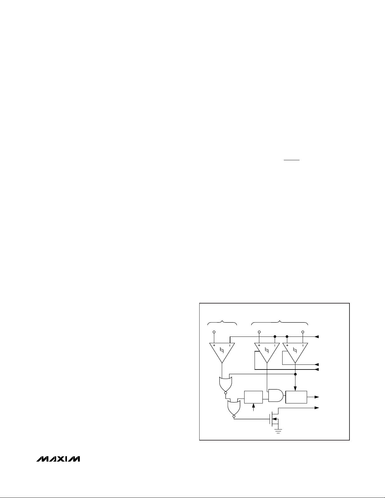
Power-Good Output (PGOOD_)
PGOOD_ is the open-drain output of a comparator that
continuously monitors both SMPS output voltages and
the auxiliary LDO output for undervoltage conditions.
PGOOD_ is actively held low in shutdown (SHDN =
GND), standby (ON3 = ON5 = ONA = GND), soft-start,
and soft-shutdown. Once the soft-start sequence terminates, PGOOD_ becomes high impedance as long as
the outputs are above 90% of the nominal regulation voltage set by FB_. PGOOD_ goes low once the respective
output drops 10% below its nominal regulation point, an
SMPS output overvoltage fault occurs, or ON_ or SHDN
is low. For a logic-level PGOOD_ output voltage, connect
an external pullup resistor between PGOOD_ and LDO5.
A 100kΩ pullup resistor works well in most applications.
Figure 6. Power-Good and Fault Protection
VV
GS TH IN
()
⎛
>
⎜
⎝
C
C
RSS
ISS
⎞
⎟
⎠
POWER GOOD
0.9 x INT REF_
0.7 x INT REF_ 1.11 x INT REF_
6144
CLK
POR
FAULT
PROTECTION
FAULT
LATCH
INTERNAL FB
ENABLE OVP
ENABLE UVP
FAULT
POWER-GOOD
Page 24

MAX8744A/MAX8745A
High-Efficiency, Quad Output, Main PowerSupply Controllers for Notebook Computers
24 ______________________________________________________________________________________
Fault Protection
Output Overvoltage Protection (OVP)—
MAX8744A Only
If the output voltage of either SMPS rises above 111% of
its nominal regulation voltage and the OVP protection is
enabled, the controller sets the fault latch, pulls PGOOD
low, shuts down the SMPS controllers that tripped the
fault, and immediately pulls DH_ low and forces DL_
high. This turns on the synchronous-rectifier MOSFETs
with 100% duty, rapidly discharging the output capacitors and clamping both outputs to ground. However,
immediately latching DL_ high typically causes slightly
negative output voltages due to the energy stored in the
output LC at the instant the OVP occurs. If the load cannot tolerate a negative voltage, place a power Schottky
diode across the output to act as a reverse-polarity
clamp. If the condition that caused the overvoltage persists (such as a shorted high-side MOSFET), the battery
blows. The other output is shut down using the soft-shutdown sequence. Cycle LDO5 below 1V or toggle either
ON3, ON5, or SHDN to clear the fault latch and restart
the SMPS controllers.
Output Undervoltage Protection (UVP)
Each SMPS controller includes an output UVP protection circuit that begins to monitor the output 6144 clock
cycles (1 / f
OSC
) after that output is enabled (ON_
pulled high). If either SMPS output voltage drops below
70% of its nominal regulation voltage and the UVP protection is enabled, the UVP circuit sets the fault latch,
pulls PGOOD low, and shuts down both controllers
using the soft-shutdown sequence. When an SMPS output voltage drops to 0.1V, its synchronous rectifier
turns on, clamping the discharged output to GND.
Cycle LDO5 below 1V or toggle either ON3, ON5, or
SHDN to clear the fault latch and restart the SMPS controllers.
Thermal-Fault Protection
The MAX8744A/MAX8745A feature a thermal fault-protection circuit. When the junction temperature rises
above +160°C, a thermal sensor activates the fault
latch, pulls PGOOD low, and shuts down both SMPS
controllers using the soft-shutdown sequence. When an
SMPS output voltage drops to 0.1V, its synchronous
rectifier turns on, clamping the discharged output to
GND. Toggle either ON3, ON5, or SHDN to clear the
fault latch and restart the controllers after the junction
temperature cools by 15°C.
Table 5. Operating Modes Truth Table
MODE CONDITION COMMENT
Transitions to discharge mode after V
Power-Up LDO5 < UVLO threshold
Run SHDN = high, ON3 or ON5 enabled Normal operation.
Output Overvoltage
(OVP) Protection
(MAX8744A)
Output Undervoltage
Protection (UVP)
Standby
Shutdown SHDN = low All circuitry off.
Thermal Shutdown TJ > +160°C
Either output > 111% of nominal level Exited by POR or cycling SHDN, ON3, or ON5.
Either output < 70% of nominal level,
UVP is enabled 6144 clock cycles
(1 / f
ON5 and ON3 < startup threshold,
SHDN = high
) after the output is enabled
OSC
Switchover Fault
Excessive current on LDO5 switchover
transistors
becomes valid. LDO5, REF remain active. DL_ is active
(high).
Exited by POR or cycling SHDN, ON3, or ON5.
DL_ stays high. LDO5 active.
Exited by POR or cycling SHDN, ON3, or ON5.
DL3 and DL5 go high before LDO5 turns off. They remain
high as long as possible thereafter.
Exited by POR or cycling SHDN, ON3, or ON5.
POR and after REF
IN
Page 25

MAX8744A/MAX8745A
High-Efficiency, Quad Output, Main Power-
Supply Controllers for Notebook Computers
______________________________________________________________________________________ 25
Auxiliary LDO Detailed Description
The MAX8744A/MAX8745A include an auxiliary linear
regulator (OUTA) that can be configured for 12V, ideal for
PCMCIA power requirements, and for biasing the gates
of load switches in a portable device. OUTA can also be
configured for outputs from 1V to 23V. The auxiliary regulator has an independent ON/OFF control, allowing it to
be shut down when not needed, reducing power consumption when the system is in a low-power state.
A flyback-winding control loop regulates a secondary
winding output, improving cross-regulation when the primary output is lightly loaded or when there is a low inputoutput differential voltage. If V
DRVA
< V
OUTA
, the
low-side switch is turned on for a time equal to 33% of
the switching period. This reverses the inductor (primary)
current, pulling current from the output filter capacitor
and causing the flyback transformer to operate in forward mode. The low impedance presented by the transformer secondary in forward mode dumps current into
the secondary output, charging up the secondary
capacitor and bringing V
INA
- V
OUTA
back into regulation. The secondary feedback loop does not improve
secondary output accuracy in normal flyback mode,
where the main (primary) output is heavily loaded. In this
condition, secondary output accuracy is determined by
the secondary rectifier drop, transformer turns ratio, and
accuracy of the main output voltage.
SMPS Design Procedure
Firmly establish the input voltage range and maximum
load current before choosing a switching frequency
and inductor operating point (ripple-current ratio). The
primary design trade-off lies in choosing a good switching frequency and inductor operating point, and the following four factors dictate the rest of the design:
• Input Voltage Range. The maximum value
(V
IN(MAX)
) must accommodate the worst-case, high
AC-adapter voltage. The minimum value (V
IN(MIN)
)
must account for the lowest battery voltage after
drops due to connectors, fuses, and battery selector
switches. If there is a choice at all, lower input voltages result in better efficiency.
• Maximum Load Current. There are two values to
consider. The peak load current (I
LOAD(MAX)
)
determines the instantaneous component stresses
and filtering requirements and thus drives output
capacitor selection, inductor saturation rating, and
the design of the current-limit circuit. The continuous load current (I
LOAD
) determines the thermal
stresses and thus drives the selection of input
capacitors, MOSFETs, and other critical heat-contributing components.
• Switching Frequency. This choice determines the
basic trade-off between size and efficiency. The optimal frequency is largely a function of maximum input
voltage, due to MOSFET switching losses that are
proportional to frequency and V
IN
2
. The optimum frequency is also a moving target, due to rapid improvements in MOSFET technology that are making higher
frequencies more practical.
• Inductor Operating Point. This choice provides
trade-offs between size vs. efficiency and transient
response vs. output ripple. Low inductor values provide better transient response and smaller physical
size, but also result in lower efficiency and higher output ripple due to increased ripple currents. The minimum practical inductor value is one that causes the
circuit to operate at the edge of critical conduction
(where the inductor current just touches zero with
every cycle at maximum load). Inductor values lower
than this grant no further size-reduction benefit. The
optimum operating point is usually found between
20% and 50% ripple current. When pulse skipping
(SKIP low and light loads), the inductor value also
determines the load-current value at which
PFM/PWM switchover occurs.
Inductor Selection
The switching frequency and inductor operating point
determine the inductor value as follows:
For example: I
LOAD(MAX)
= 5A, VIN= 12V, V
OUT
= 5V,
f
OSC
= 300kHz, 30% ripple current or LIR = 0.3:
Find a low-loss inductor having the lowest possible DC
resistance that fits in the allotted dimensions. Most inductor manufacturers provide inductors in standard values,
such as 1.0µH, 1.5µH, 2.2µH, 3.3µH, etc. Also look for
non-standard values, which can provide a better compromise in LIR across the input voltage range. If using a
swinging inductor (where the no-load inductance
decreases linearly with increasing current), evaluate the
LIR with properly scaled inductance values. For the
selected inductance value, the actual peak-to-peak
inductor ripple current (ΔI
INDUCTOR
) is defined by:
L
12 300 5 0 3
ΔI
INDUCTOR
VVV
OUT IN OUT
L
=
V f I LIR
IN OSCLOAD MAX
Vx V V
5125
()
V x kHz x A x
−
()
−
VVV
OUT IN OUT
=
()
=μ
650..
−()
Vf L
IN OSC
H=
Page 26

MAX8744A/MAX8745A
High-Efficiency, Quad Output, Main PowerSupply Controllers for Notebook Computers
26 ______________________________________________________________________________________
Ferrite cores are often the best choice, although powdered iron is inexpensive and can work well at 200kHz.
The core must be large enough not to saturate at the
peak inductor current (I
PEAK
):
Transformer Design (for
MAX8744A/MAX8745A Auxiliary Output)
A coupled inductor or transformer can be substituted
for the inductor in the 5V SMPS to create an auxiliary
output (Figure 1). The MAX8744A/MAX8745A is particularly well suited for such applications because the
secondary feedback threshold automatically triggers
DL5 even if the 5V output is lightly loaded.
The power requirements of the auxiliary supply must be
considered in the design of the main output. The transformer must be designed to deliver the required current
in both the primary and the secondary outputs with the
proper turns ratio and inductance. The power ratings of
the synchronous-rectifier MOSFETs and the current limit
in the MAX8744A/MAX8745A must also be adjusted
accordingly. Extremes of low input-output differentials,
widely different output loading levels, and high turns
ratios can further complicate the design due to parasitic
transformer parameters such as interwinding capacitance, secondary resistance, and leakage inductance.
Power from the main and secondary outputs is combined to get an equivalent current referred to the main
output. Use this total current to determine the current
limit (see the
Setting the Current Limit
section):
I
TOTAL
= P
TOTAL
/ V
OUT5
where I
TOTAL
is the equivalent output current referred
to the main output, and P
TOTAL
is the sum of the output
power from both the main output and the secondary
output:
where L
PRIMARY
is the primary inductance, N is the
transformer turns ratio, V
SEC
is the minimum required
rectified secondary voltage, V
FWD
is the forward drop
across the secondary rectifier, V
OUT5(MIN)
is the mini-
mum value of the main output voltage, and V
RECT
is the
on-state voltage drop across the synchronous-rectifier
MOSFET. The transformer secondary return is often connected to the main output voltage instead of ground in
order to reduce the necessary turns ratio. In this case,
subtract V
OUT5
from the secondary voltage (V
SEC
-
V
OUT5
) in the transformer turns-ratio equation above. The
secondary diode in coupled-inductor applications must
withstand flyback voltages greater than 60V. Common
silicon rectifiers, such as the 1N4001, are also prohibited
because they are too slow. Fast silicon rectifiers such as
the MURS120 are the only choice. The flyback voltage
across the rectifier is related to the V
IN
- V
OUT5
differ-
ence, according to the transformer turns ratio:
V
FLYBACK
= V
SEC
+ (VIN– V
OUT5
) x N
where N is the transformer turns ratio (secondary windings/primary windings), and V
SEC
is the maximum secondary DC output voltage. If the secondary winding is
returned to V
OUT5
instead of ground, subtract V
OUT5
from V
FLYBACK
in the equation above. The diode’s
reverse breakdown voltage rating must also accommodate any ringing due to leakage inductance. The
diode’s current rating should be at least twice the DC
load current on the secondary output.
Transient Response
The inductor ripple current also impacts transientresponse performance, especially at low VIN- V
OUT
differentials. Low inductor values allow the inductor
current to slew faster, replenishing charge removed
from the output filter capacitors by a sudden load step.
The total output voltage sag is the sum of the voltage
sag while the inductor is ramping up, and the voltage
sag before the next pulse can occur:
where D
MAX
is maximum duty factor (see the
Electrical
Characteristics
), T is the switching period (1 / f
OSC
), and
ΔT equals V
OUT
/ VINx T when in PWM mode, or L x 0.2 x
I
MAX
/ (VIN- V
OUT
) when in skip mode. The amount of
overshoot during a full-load to no-load transient due to
stored inductor energy can be calculated as:
Setting the Current Limit
The minimum current-limit threshold must be great
enough to support the maximum load current when the
current limit is at the minimum tolerance value. The
peak inductor current occurs at I
LOAD(MAX)
plus half
the ripple current; therefore:
II
=+
PEAK LOAD MAX
()
Δ
I
INDUCTOR
2
N
=
VVV
VV
+
SEC FWD
++
5
OUT RECT SENSE
LI
Δ
()
V
SAG
=
2
CVxD V
ΔΔ
ITT
LOAD MAX
()
OUT IN MAX OUT
LOAD MAX
()
()
C
OUT
2
()
−
−
IL
Δ
()
V
SOAR
≈
2
LOAD MAX
CV
2
()
II
>
LIMIT LOAD MAX
()
I
Δ
⎛
INDUCTOR
+
⎜
⎝
2
+
⎞
⎟
⎠
Page 27

where I
LIMIT_
equals the minimum current-limit threshold voltage divided by the current-sense resistance
(R
SENSE_
). For the default setting, the minimum current-
limit threshold is 45mV.
Connect ILIM to LDO5 for a default 50mV current-limit
threshold. In adjustable mode, the current-limit threshold is precisely 1/10 the voltage seen at ILIM. For an
adjustable threshold, connect a resistive divider from
REF to analog ground (GND) with ILIM connected to
the center tap. The external 0.5V to 2V adjustment
range corresponds to a 50mV to 200mV current-limit
threshold. When adjusting the current limit, use 1% tolerance resistors and a divider current of approximately
10mA to prevent significant inaccuracy in the currentlimit tolerance.
The current-sense method (Figure 7) and magnitude
determines the achievable current-limit accuracy and
power loss. Typically, higher current-sense limits provide tighter accuracy, but also dissipate more power.
Most applications employ a current-limit threshold
(V
LIMIT
) of 50mV to 100mV, so the sense resistor may
be determined by:
For the best current-sense accuracy and overcurrent
protection, use a 1% tolerance current-sense resistor
between the inductor and output as shown in Figure
7A. This configuration constantly monitors the inductor
MAX8744A/MAX8745A
High-Efficiency, Quad Output, Main Power-
Supply Controllers for Notebook Computers
______________________________________________________________________________________ 27
Figure 7. Current-Sense Configurations
C
IN
MAX8744A
MAX8745A
DH_
LX_
DL_
PGND
N
H
N
L
L
D
L
V
R
LIMIT
==
CS
I
LIMIT
10
V
xI
ILIM
LIMIT
INPUT (V
)
IN
SENSE RESISTOR
L
ESL
R1
R
SENSE
C
L
R
ESL
SENSE
CEQR1 =
C
EQ
OUT
CSH_
CSL_
A) OUTPUT SERIES RESISTOR SENSING
MAX8744A
MAX8745A
B) LOSSLESS INDUCTOR SENSING
DH_
LX_
DL_
PGND
CSH_
CSL_
INPUT (VIN)
C
IN
N
H
N
L
D
L
INDUCTOR
LR
R1
DCR
R2
C
EQ
RCS =R
(
R1 + R2
C
OUT
L
R
=
DCR
C
EQ
R2
[
)
1R11
+
R2
DCR
]
Page 28

MAX8744A/MAX8745A
High-Efficiency, Quad Output, Main PowerSupply Controllers for Notebook Computers
28 ______________________________________________________________________________________
current, allowing accurate current-limit protection.
However, the parasitic inductance of the current-sense
resistor can cause current-limit inaccuracies, especially
when using low-value inductors and current-sense
resistors. This parasitic inductance (L
ESL
) can be canceled by adding an RC circuit across the sense resistor
with an equivalent time constant:
Alternatively, high-power applications that do not
require highly accurate current-limit protection may
reduce the overall power dissipation by connecting a
series RC circuit across the inductor (Figure 7B) with
an equivalent time constant:
and:
where RCSis the required current-sense resistance,
and R
DCR
is the inductor’s series DC resistance. Use
the typical inductance and R
DCR
values provided by
the inductor manufacturer.
Output Capacitor Selection
The output filter capacitor must have low enough equivalent series resistance (ESR) to meet output ripple and
load-transient requirements, yet have high enough ESR to
satisfy stability requirements. The output capacitance
must be high enough to absorb the inductor energy while
transitioning from full-load to no-load conditions without
tripping the overvoltage fault protection. When using high
capacitance, low-ESR capacitors (see stability requirements), the filter capacitor’s ESR dominates the output
voltage ripple. So the output capacitor’s size depends on
the maximum ESR required to meet the output voltage
ripple (V
RIPPLE(P-P)
) specifications:
V
RIPPLE(P-P)
= R
ESR
I
LOAD(MAX)
LIR
In idle mode, the inductor current becomes discontinuous, with peak currents set by the idle mode currentsense threshold (V
IDLE
= 0.2V
LIMIT
). In idle mode, the
no-load output ripple may be determined as follows:
The actual capacitance value required relates to the
physical size needed to achieve low ESR, as well as to
the chemistry of the capacitor technology. Thus, the
capacitor is usually selected by ESR and voltage rating
rather than by capacitance value (this is true of tantalums, OS-CONs, polymers, and other electrolytics).
When using low-capacity filter capacitors, such as
ceramic capacitors, size is usually determined by the
capacity needed to prevent V
SAG
and V
SOAR
from
causing problems during load transients. Generally,
once enough capacitance is added to meet the overshoot requirement, undershoot at the rising load edge
is no longer a problem (see the V
SAG
and V
SOAR
equa-
tions in the
Transient Response
section). However, lowcapacity filter capacitors typically have high ESR zeros
that may affect the overall stability (see the
Output-
Capacitor Stability Considerations
section).
Output-Capacitor Stability Considerations
Stability is determined by the value of the ESR zero relative to the switching frequency. The boundary of instability is given by the following equation:
where:
For a typical 300kHz application, the ESR zero frequency
must be well below 95kHz, preferably below 50kHz.
Tantalum and OS-CON capacitors in widespread use
at the time of publication have typical ESR zero frequencies of 25kHz. In the design example used for
inductor selection, the ESR needed to support 25mV
P-P
ripple is 25mV/1.5A = 16.7mΩ. One 220µF/4V Sanyo
polymer (TPE) capacitor provides 15mΩ (max) ESR.
This results in a zero at 48kHz, well within the bounds
of stability.
For low-input voltage applications where the duty cycle
exceeds 50% (V
OUT/VIN
≥ 50%), the output ripple volt-
age should not be greater than twice the internal slopecompensation voltage:
V
RIPPLE
≤ 0.02 x V
OUT
where V
RIPPLE
equals ΔI
INDUCTOR
x R
ESR
. The worst-
case ESR limit occurs when VIN= 2 x V
OUT
, so the above
equation may be simplified to provide the following
boundary condition:
R
ESR
≤ 0.04 x L x f
SW
L
1 =
ESL
R
SENSE
CR
EQ
⎛
R
=
CS DCR
⎜
RR
⎝
⎞
2
R
R
⎟
+
12
⎠
R
DCR
L
111
=+
⎡
⎢
CRR
⎣
EQ
⎤
⎥
2
⎦
V
RIPPLE P P
(–)
VR
IDLE ESR
=
R
SENSE
f
ESR
OSC
≤
π
f
f
ESR
=
RC
2π
ESR OUT
1
Page 29

MAX8744A/MAX8745A
High-Efficiency, Quad Output, Main Power-
Supply Controllers for Notebook Computers
______________________________________________________________________________________ 29
Do not put high-value ceramic capacitors directly
across the feedback sense point without taking precautions to ensure stability. Large ceramic capacitors can
have a high ESR zero frequency and cause erratic,
unstable operation. However, it is easy to add enough
series resistance by placing the capacitors a couple of
inches downstream from the feedback sense point,
which should be as close as possible to the inductor.
Unstable operation manifests itself in two related, but
distinctly different ways: short/long pulses and cycle
skipping, which results in lower frequency operation.
Instability occurs due to noise on the output or because
the ESR is so low that there is not enough voltage ramp
in the output voltage signal. This “fools” the error comparator into triggering too early or into skipping a cycle.
Cycle skipping is more annoying than harmful, resulting
in nothing worse than increased output ripple.
However, it can indicate the possible presence of loop
instability due to insufficient ESR. Loop instability can
result in oscillations at the output after line or load
steps. Such perturbations are usually damped, but can
cause the output voltage to rise above or fall below the
tolerance limits.
The easiest method for checking stability is to apply a
very fast zero-to-max load transient and carefully
observe the output-voltage-ripple envelope for overshoot and ringing. It may help to simultaneously monitor the inductor current with an AC current probe. Do
not allow more than three cycles of ringing after the initial step-response under/overshoot.
Input Capacitor Selection
The input capacitor must meet the ripple current
requirement (I
RMS
) imposed by the switching currents.
For an out-of-phase regulator, the total RMS current in
the input capacitor is a function of the load currents,
the input currents, the duty cycles, and the amount of
overlap as defined in Figure 8.
Figure 8. Input RMS Current
INPUT RMS CURRENT FOR INTERLEAVED OPERATION:
INPUT RMS CURRENT FOR SINGLE-PHASE OPERATION:
INPUT CAPACITOR RMS CURRENT
5.0
4.5
4.0
3.5
3.0
(A)
2.5
RMS
I
2.0
1.5
1.0
0.5
0
020
vs. INPUT VOLTAGE
IN PHASE
50/50 INTERLEAVING
40/60 OPTIMAL
INTERLEAVING
181612 14108
VIN (V)
IIDDIIDDIIIDIDDD
=−
RMS OUT IN LX OL OUT IN LX OL OUT OUT IN OL IN LX LX OL
D
I
IN
II
RMS LOAD
()
V
OUT
===
LX
5
V
IN
VI VI
55 33
OUT OUT OUT OUT
=
=
2
5
5
D
LX
+
V
ININ
⎛
VVV
OUT IN OUT
⎜
⎜
⎜
⎝
−
()
532353
V
OUT
3
V
−
()
V
IN
+−
()
3
D DUTY CYCLE OVERLAP FRACTION
IN
OL
⎞
⎟
⎟
⎟
⎠
−
−
()
++−
()
2
2
+−−+
1
()
53
Page 30

MAX8744A/MAX8745A
High-Efficiency, Quad Output, Main PowerSupply Controllers for Notebook Computers
30 ______________________________________________________________________________________
The 40/60 optimal interleaved architecture of the
MAX8744A/MAX8745A allows the input voltage to go
as low 8.3V before the duty cycles begin to overlap.
This offers improved efficiency over a regular 180° outof-phase architecture where the duty cycles begin to
overlap below 10V. Figure 8 shows the input-capacitor
RMS current vs. input voltage for an application that
requires 5V/5A and 3.3V/5A. This shows the improvement of the 40/60 optimal interleaving over 50/50 interleaving and in-phase operation.
For most applications, nontantalum chemistries (ceramic,
aluminum, or OS-CON) are preferred due to their resistance to power-up surge currents typical of systems
with a mechanical switch or connector in series with the
input. Choose a capacitor that has less than 10°C temperature rise at the RMS input current for optimal reliability and lifetime.
Power-MOSFET Selection
Most of the following MOSFET guidelines focus on the
challenge of obtaining high load-current capability
when using high-voltage (> 20V) AC adapters. Lowcurrent applications usually require less attention.
The high-side MOSFET (NH) must be able to dissipate
the resistive losses plus the switching losses at both
V
IN(MIN)
and V
IN(MAX)
. Ideally, the losses at V
IN(MIN)
should be roughly equal to the losses at V
IN(MAX)
, with
lower losses in between. If the losses at V
IN(MIN)
are
significantly higher, consider increasing the size of NH.
Conversely, if the losses at V
IN(MAX)
are significantly
higher, consider reducing the size of NH. If VINdoes not
vary over a wide range, maximum efficiency is achieved
by selecting a high-side MOSFET (NH) that has conduction losses equal to the switching losses.
Choose a low-side MOSFET (NL) that has the lowest possible on-resistance (R
DS(ON)
), comes in a moderate-sized
package (i.e., 8-pin SO, DPAK, or D2PAK), and is reasonably priced. Ensure that the MAX8744A/MAX8745A DL_
gate driver can supply sufficient current to support the
gate charge and the current injected into the parasitic
drain-to-gate capacitor caused by the high-side MOSFET
turning on; otherwise, cross-conduction problems may
occur. Switching losses are not an issue for the low-side
MOSFET since it is a zero-voltage switched device when
used in the step-down topology.
Power-MOSFET Dissipation
Worst-case conduction losses occur at the duty-factor
extremes. For the high-side MOSFET (NH), the worstcase power dissipation due to resistance occurs at minimum input voltage:
Generally, use a small high-side MOSFET to reduce
switching losses at high input voltages. However, the
R
DS(ON)
required to stay within package power-dissipation limits often limits how small the MOSFET can be. The
optimum occurs when the switching losses equal the
conduction (R
DS(ON)
) losses. High-side switching losses
do not become an issue until the input is greater than
approximately 15V.
Calculating the power dissipation in high-side MOSFETs
(NH) due to switching losses is difficult, since it must
allow for difficult-to-quantify factors that influence the turnon and turn-off times. These factors include the internal
gate resistance, gate charge, threshold voltage, source
inductance, and PCB layout characteristics. The following
switching-loss calculation provides only a very rough estimate and is no substitute for breadboard evaluation,
preferably including verification using a thermocouple
mounted on NH:
where C
OSS
is the output capacitance of NH, Q
G(SW)
is
the charge needed to turn on the NH MOSFET, and I
GATE
is the peak gate-drive source/sink current (1A typ).
Switching losses in the high-side MOSFET can become
a heat problem when maximum AC adapter voltages
are applied, due to the squared term in the switchingloss equation (C x V
IN
2
x fSW). If the high-side MOSFET
chosen for adequate R
DS(ON)
at low battery voltages
becomes extraordinarily hot when subjected to
V
IN(MAX)
, consider choosing another MOSFET with
lower parasitic capacitance.
For the low-side MOSFET (NL), the worst-case power
dissipation always occurs at maximum battery voltage:
The absolute worst case for MOSFET power dissipation
occurs under heavy overload conditions that are
greater than I
LOAD(MAX)
, but are not high enough to
exceed the current limit and cause the fault latch to trip.
To protect against this possibility, “overdesign” the circuit to tolerate:
PD N sistive
()
H
PD N Switching
()
H
IQICV
⎛
LOAD G SW
⎜
⎝
() ( )
GATE
PD N sistive
()
L
⎡
⎛
−
1
⎢
⎜
⎝
⎢
⎣
⎛
=
⎜
⎝
=
+
Re
V
OUT
V
IN MAX
()
⎞
V
OUT
()
⎟
V
⎠
IN
OSS IN MAX
2
=
⎤
⎞
IR
⎥
()
LOAD DS ON
⎟
⎠
⎥
⎦
2
IR
LOAD DS ONRe()
⎞
Vf
IN MAX SW
⎟
⎠
2
()
()
Page 31

MAX8744A/MAX8745A
High-Efficiency, Quad Output, Main Power-
Supply Controllers for Notebook Computers
______________________________________________________________________________________ 31
where I
LIMIT
is the peak current allowed by the currentlimit circuit, including threshold tolerance and senseresistance variation. The MOSFETs must have a relatively
large heatsink to handle the overload power dissipation.
Choose a Schottky diode (DL) with a forward-voltage
drop low enough to prevent the low-side MOSFET’s
body diode from turning on during the dead time. As a
general rule, select a diode with a DC current rating
equal to a 1/3 the load current. This diode is optional
and can be removed if efficiency is not critical.
Boost Capacitors
The boost capacitors (C
BST
) must be selected large
enough to handle the gate-charging requirements of
the high-side MOSFETs. Typically, 0.1µF ceramic
capacitors work well for low-power applications driving
medium-sized MOSFETs. However, high-current applications driving large, high-side MOSFETs require boost
capacitors larger than 0.1µF. For these applications,
select the boost capacitors to avoid discharging the
capacitor more than 200mV while charging the highside MOSFETs’ gates:
where Q
GATE
is the total gate charge specified in the
high-side MOSFET’s data sheet. For example, assume
the FDS6612A n-channel MOSFET is used on the high
side. According to the manufacturer’s data sheet, a single FDS6612A has a maximum gate charge of 13nC
(V
GS
= 5V). Using the above equation, the required
boost capacitance would be:
Selecting the closest standard value, this example
requires a 0.1µF ceramic capacitor.
LDOA Design Procedure
Output Voltage Selection
Adjust the auxiliary linear regulator’s output voltage by
connecting a resistive divider between OUTA and analog ground with the center tap connected to FBA
(Figure 1). Select R6 in the 10kΩ to 30kΩ range, and
calculate R5 with the following equation:
where V
FBA
= 1.0V.
Transistor Selection
The pass transistor must meet specifications for current
gain (β), input capacitance, collector-emitter saturation
voltage, and power dissipation. The transistor’s current
gain limits the guaranteed maximum output current to:
where I
DRV
is the minimum guaranteed base drive current, VBEis the base-to-emitter voltage of the transistor,
and R
BE
is the pullup resistor connected between the
transistor’s base and emitter. Furthermore, the transistor’s current gain increases the linear regulator’s DC
loop gain (see the
LDOA Stability Requirements
section), so excessive gain destabilizes the output.
Therefore, transistors with current gain over 100 at the
maximum output current can be difficult to stabilize and
are not recommended. The transistor’s input capacitance and input resistance also create a second pole,
which could be low enough to make the output unstable when heavily loaded.
The transistor’s saturation voltage at the maximum output current determines the minimum input-to-output
voltage differential that the linear regulator supports.
Alternatively, the package’s power dissipation could
limit the useable maximum input-to-output voltage differential. The maximum power dissipation capability of
the transistor’s package and mounting must exceed the
actual power dissipation in the device. The power dissipation equals the maximum load current times the maximum input-to-output differential:
PWR = I
LOAD(MAX)(VINA-VOUTA
)
PWR = I
LOAD(MAX)VCE
LDOA Stability Requirements
The MAX8744A/MAX8745A linear-regulator controller
uses an internal transconductance amplifier to drive an
external pnp pass transistor. The transconductance
amplifier, the pass transistor, the base-to-emitter resistor,
and the output capacitor determine the loop stability.
The transconductance amplifier regulates the output
voltage by controlling the pass transistor’s base current. The total DC loop gain is approximately:
where VTis 26mV at room temperature, hFEis the pass
transistor’s DC gain, and I
BIAS
is the current through
the base-to-emitter resistor (RBE). The 680Ω base-toemitter resistor used in Figure 1 was chosen to provide
a 1mA bias current (I
BIAS
).
I
Δ
⎛
II
=−
LOAD LIMIT
INDUCTOR
⎜
⎝
2
⎞
⎟
⎠
C
C
==μ
BST
Q
GATE
=
BST
200
mV
nC
13
200
mV
F
0 065.
RR
⎛
V
⎜
⎝
OUTA
V
FBA
56 1=−
⎞
⎟
⎠
II
LOAD MAX DRV
=
()
⎜
⎝
⎛
⎞
V
BE
β
−
MIN
⎟
R
⎠
BE
A
V LDO
()
=
⎛
⎜
⎝
.
55
V
⎞
⎛
V
T
Ih
BIAS FE
+
1
⎟
⎜
I
⎠
⎝
LOAD
⎞
⎟
⎠
Page 32

MAX8744A/MAX8745A
High-Efficiency, Quad Output, Main PowerSupply Controllers for Notebook Computers
32 ______________________________________________________________________________________
The output capacitor and the load resistance create the
dominant pole in the system. However, the internal amplifier delay, the pass transistor’s input capacitance, and the
stray capacitance at the feedback node create additional
poles in the system, and the output capacitor’s ESR generates a zero. For proper operation, use the following
steps to ensure the linear-regulator stability:
1) First, calculate the dominant pole set by the linear
regulator’s output capacitor and the load resistor:
where C
OUTA
is the output capacitance of the aux-
iliary LDO and R
LOAD
is the load resistance corresponding to the maximum load current. The unitygain crossover of the linear regulator is:
f
CROSSOVER
= A
V(LDO)fPOLE(LDO)
2) The pole caused by the internal amplifier delay is at
approximately 1MHz:
f
POLE(AMP)
≈ 1MHz
3) Next, calculate the pole set by the transistor’s input
capacitance, the transistor’s input resistance, and
the base-to-emitter pullup resistor. Since the transistor’s input resistance (hFE/gm) is typically much
greater than the base-to-emitter pullup resistance,
the pole can be determined from the simplified
equation:
where gmis the transconductance of the pass transistor, and fTis the transition frequency. Both parameters can be found in the transistor’s data sheet.
Therefore, the equation can be further reduced to:
4) Next, calculate the pole set by the linear regulator’s
feedback resistance and the capacitance between
FBA and ground (approximately 5pF including
stray capacitance):
5) Next, calculate the zero caused by the output
capacitor’s ESR:
where R
ESR
is the equivalent series resistance of
C
OUTA
.
6) To ensure stability, choose C
OUTA
large enough so
that the crossover occurs well before the poles and
zero calculated in steps 2 through 5. The poles in
steps 3 and 4 generally occur at several MHz, and
using ceramic output capacitors ensures the ESR
zero occurs at several MHz as well. Placing the
crossover frequency below 500kHz is typically sufficient to avoid the amplifier delay pole and generally works well, unless unusual component
selection or extra capacitance moves the other
poles or zero below 1MHz.
A capacitor connected between the linear regulator’s output and the feedback node can improve
the transient response and reduce the noise coupled into the feedback loop.
If a low-dropout solution is required, an external
p-channel MOSFET pass transistor could be used.
However, a pMOS-based linear regulator requires
higher output capacitance to stabilize the loop. The
high gate capacitance of the p-channel MOSFET
lowers the f
POLE(CIN)
and can cause instability. A
large output capacitance must be used to reduce
the unity-gain bandwidth and ensure that the pole
is well above the unity-gain crossover frequency.
Applications Information
Duty-Cycle Limits
Minimum Input Voltage
The minimum input operating voltage (dropout voltage) is
restricted by the maximum duty-cycle specification (see
the
Electrical Characteristics
table). However, keep in
mind that the transient performance gets worse as the
step-down regulators approach the dropout voltage, so
bulk output capacitance must be added (see the voltage
sag and soar equations in the
Transient Response
sec-
tion of the
SMPS Design Procedure
section). The
absolute point of dropout occurs when the inductor current ramps down during the off-time (ΔI
DOWN
) as much
as it ramps up during the on-time (ΔI
UP
). This results in a
minimum operating voltage defined by the following
equation:
1
f
POLE LDO
()
=
2π
1
CR
OUTA LOAD
f
POLE CIN
()
≈
CR
22π
IN IN
g
IN
m
=
π
f
T
C
f
f
POLE CIN
()
T
≈
h
FE
f
POLE FBA
()
=
256π
1
CRR
(||)
FBA
f
ZERO ESR
()
=
1
CR
2π
OUTA ESR
Page 33

MAX8744A/MAX8745A
High-Efficiency, Quad Output, Main Power-
Supply Controllers for Notebook Computers
______________________________________________________________________________________ 33
where V
CHG
and V
DIS
are the parasitic voltage drops in
the charge and discharge paths, respectively. A reasonable minimum value for h is 1.5, while the absolute
minimum input voltage is calculated with h = 1.
Maximum Input Voltage
The MAX8744A/MAX8745A controllers include a minimum on-time specification, which determines the maximum input operating voltage that maintains the
selected switching frequency (see the
Electrical
Characteristics
table). Operation above this maximum
input voltage results in pulse-skipping operation,
regardless of the operating mode selected by SKIP. At
the beginning of each cycle, if the output voltage is still
above the feedback threshold voltage, the controller
does not trigger an on-time pulse, effectively skipping a
cycle. This allows the controller to maintain regulation
above the maximum input voltage, but forces the controller to effectively operate with a lower switching frequency. This results in an input threshold voltage at
which the controller begins to skip pulses (V
IN(SKIP)
):
where f
OSC
is the switching frequency selected by FSEL.
PCB Layout
Careful PCB layout is critical to achieving low switching
losses and clean, stable operation. The switching
power stage requires particular attention (Figure 9). If
possible, mount all the power components on the top
side of the board, with their ground terminals flush
against one another. Follow these guidelines for good
PCB layout:
• Keep the high-current paths short, especially at the
ground terminals. This practice is essential for stable, jitter-free operation.
• Keep the power traces and load connections short.
This practice is essential for high efficiency. Using
thick copper PCBs (2oz vs. 1oz) can enhance fullload efficiency by 1% or more. Correctly routing
PCB traces is a difficult task that must be
approached in terms of fractions of centimeters,
where a single milliohm of excess trace resistance
causes a measurable efficiency penalty.
• Minimize current-sensing errors by connecting
CSH_ and CSL_ directly across the current-sense
resistor (R
SENSE_
).
• When trade-offs in trace lengths must be made, it is
preferable to allow the inductor charging path to be
made longer than the discharge path. For example,
it is better to allow some extra distance between the
input capacitors and the high-side MOSFET than to
allow distance between the inductor and the lowside MOSFET or between the inductor and the output filter capacitor.
• Route high-speed switching nodes (BST_, LX_,
DH_, and DL_) away from sensitive analog areas
(REF, FB_, CSH_, CSL_).
Layout Procedure
Place the power components first, with ground terminals adjacent (NL_ source, CIN, C
OUT
_, and DL_
anode). If possible, make all these connections on the
top layer with wide, copper-filled areas.
Mount the controller IC adjacent to the low-side MOSFET,
preferably on the back side opposite NL_and NH_to
keep LX_, GND, DH_, and the DL_ gate-drive lines short
and wide. The DL_ and DH_ gate traces must be short
and wide (50 mils to 100 mils wide if the MOSFET is 1in
from the controller IC) to keep the driver impedance low
and for proper adaptive dead-time sensing.
Group the gate-drive components (BST_ capacitor,
LDO5 bypass capacitor) together near the controller IC.
Make the DC-DC controller ground connections as
shown in Figures 1 and 9. This diagram can be viewed
as having two separate ground planes: power ground,
where all the high-power components go, and an analog ground plane for sensitive analog components. The
analog ground plane and power ground plane must
meet only at a single point directly at the IC.
Connect the output power planes directly to the output
filter capacitor positive and negative terminals with multiple vias. Place the entire DC-DC converter circuit as
close to the load as is practical.
⎛
VVVhDVV
IN MIN OUT CHG
1
⎜
⎝
MAX
⎞
1
=++ −
⎟
⎠
+
()
OUT DIS()
VV
IN SKIP OUT
()
⎛
=
⎜
⎝
1
ft
OSC ON MIN
()
⎞
⎟
⎠
Page 34
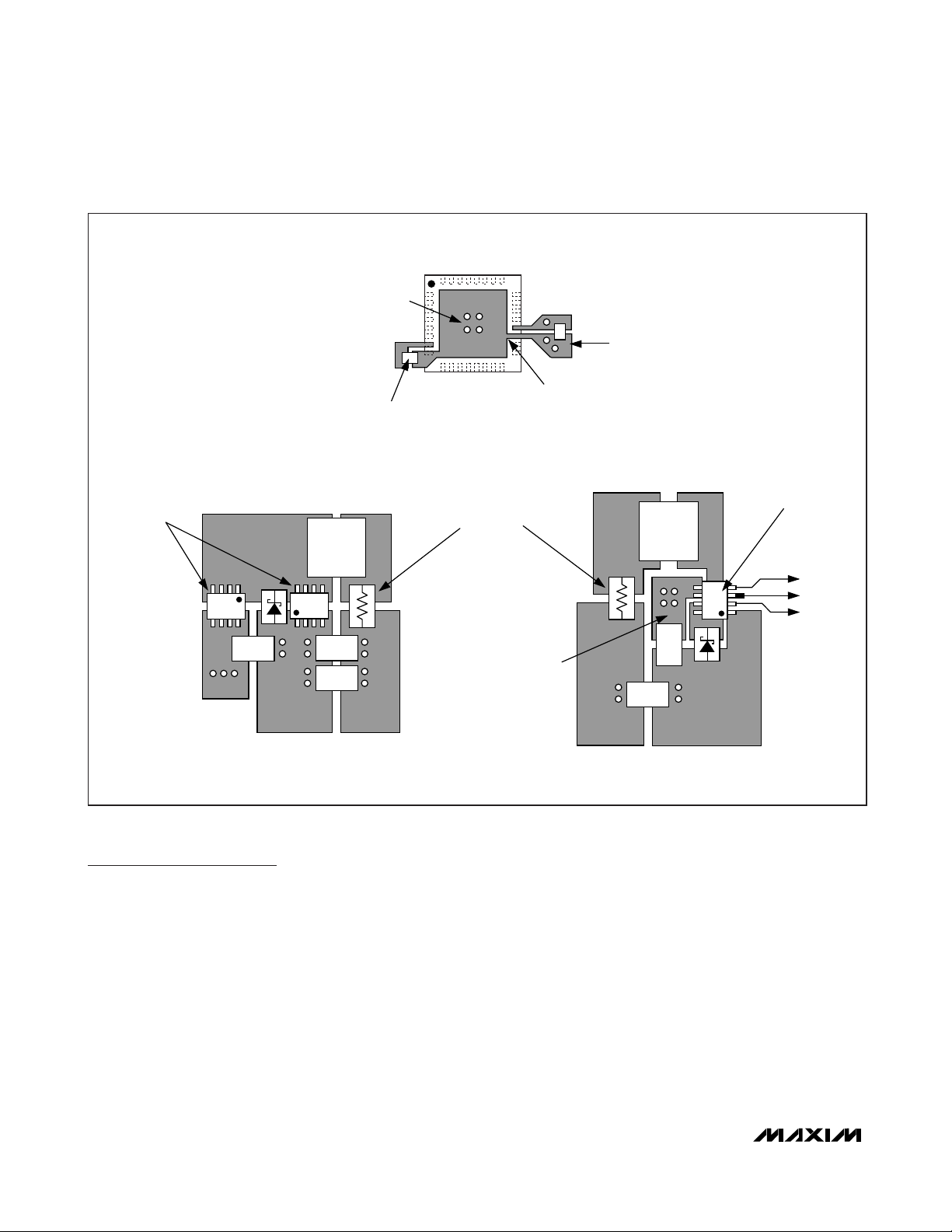
MAX8744A/MAX8745A
High-Efficiency, Quad Output, Main PowerSupply Controllers for Notebook Computers
34 ______________________________________________________________________________________
Figure 9. PCB Layout
Chip Information
TRANSISTOR COUNT: 6897
PROCESS: BiCMOS
MAX8744A/MAX8745A
CONNECT THE
EXPOSED PAD TO
ANALOG GND
VIA TO POWER
GROUND
CONNECT GND AND PGND TO THE
REF BYPASS
CAPACITOR
CONTROLLER AT ONE POINT
ONLY AS SHOWN
SINGLE
n-CHANNEL
MOSFETS
INDUCTOR
(REFER TO THE EVALUATION KIT)
C
IN
INPUT
HIGH-POWER LAYOUT LOW-POWER LAYOUT
GROUND OUTPUT
C
OUT
C
OUT
KELVIN SENSE VIAS
UNDER THE SENSE
RESISTOR
INPUT
OUTPUT
INDUCTOR
C
OUT
DUAL
n-CHANNEL
MOSFET
DH
LX
DL
C
IN
GROUND
Page 35

MAX8744A/MAX8745A
High-Efficiency, Quad Output, Main Power-
Supply Controllers for Notebook Computers
______________________________________________________________________________________ 35
Package Information
(The package drawing(s) in this data sheet may not reflect the most current specifications. For the latest package outline information
go to www.maxim-ic.com/packages
.)
QFN THIN.EPS
Page 36

MAX8744A/MAX8745A
High-Efficiency, Quad Output, Main PowerSupply Controllers for Notebook Computers
Maxim cannot assume responsibility for use of any circuitry other than circuitry entirely embodied in a Maxim product. No circuit patent licenses are
implied. Maxim reserves the right to change the circuitry and specifications without notice at any time.
36
Maxim Integrated Products, 120 San Gabriel Drive, Sunnyvale, CA 94086 408-737-7600
© 2007 Maxim Integrated Products is a registered trademark of Maxim Integrated Products, Inc.
Package Information (continued)
(The package drawing(s) in this data sheet may not reflect the most current specifications. For the latest package outline information
go to www.maxim-ic.com/packages
.)
 Loading...