Maxim MAX8732EEI, MAX8733EEI, MAX8734EEI Schematics
General Description
The MAX8732/MAX8733/MAX8734 dual step-down,
switch-mode power-supply (SMPS) controllers generate
logic-supply voltages in battery-powered systems. The
MAX8732/MAX8733/MAX8734 include two pulse-width
modulation (PWM) controllers, adjustable from 2V to 5.5V
or fixed at 5V and 3.3V. These devices feature two linear
regulators providing 5V and 3.3V always-on outputs. Each
linear regulator provides up to 100mA output current with
automatic linear-regulator bootstrapping to the main
SMPS outputs. The MAX8732/MAX8733/MAX8734 include
on-board power-up sequencing, a power-good (PGOOD)
output, digital soft-start, and internal soft-stop output discharge that prevents negative voltages on shutdown.
Maxim’s proprietary Quick-PWM™ quick-response, constant on-time PWM control scheme operates without
sense resistors and provides 100ns response to load transients while maintaining a relatively constant switching frequency. The unique ultrasonic pulse-skipping mode
maintains the switching frequency above 25kHz, which
eliminates noise in audio applications. Other features
include pulse skipping, which maximizes efficiency in
light-load applications, and fixed-frequency PWM mode,
which reduces RF interference in sensitive applications.
The MAX8732 features a 200kHz/5V and 300kHz/3.3V
SMPS for highest efficiency, while the MAX8733 features
a 400kHz/5V and 500kHz/3.3V SMPS for “thin and light”
applications. The MAX8734 provides a pin-selectable
switching frequency, allowing either 200kHz/300kHz or
400kHz/500kHz operation of the 5V/3.3V SMPSs, respectively. The MAX8732/MAX8733/MAX8734 are available in
28-pin QSOP packages and operate over the extended
temperature range (-40°C to +85°C).
The MAX8732/MAX8733/MAX8734 are pin-for-pin
upgrades to the MAX1777/MAX1977/MAX1999.
The MAX1999 Evaluation Kit can be used to evaluate
the MAX8732/MAX8733/MAX8734.
Applications
Notebook and Subnotebook Computers
PDAs and Mobile Communication Devices
3- and 4-Cell Li+ Battery-Powered Devices
Features
♦ No Current-Sense Resistor Needed (MAX8734)
♦ Accurate Current Sense with Current-Sense
Resistor (MAX8732/MAX8733)
♦ 1.5% Output Voltage Accuracy
♦ 3.3V and 5V 100mA Bootstrapped Linear
Regulators
♦ Internal Soft-Start and Soft-Stop Output
Discharge
♦ Quick-PWM with 100ns Load Step Response
♦ 3.3V and 5V Fixed or Adjustable Outputs
(Dual Mode™)
♦ 4.5V to 24V Input Voltage Range
♦ Enhanced Ultrasonic Pulse-Skipping Mode
(25kHz min)
♦ Power-Good (PGOOD) Signal
♦ Overvoltage Protection Enable/Disable
MAX8732/MAX8733/MAX8734
High-Efficiency, Quad-Output, Main Power-
Supply Controllers for Notebook Computers
________________________________________________________________ Maxim Integrated Products 1
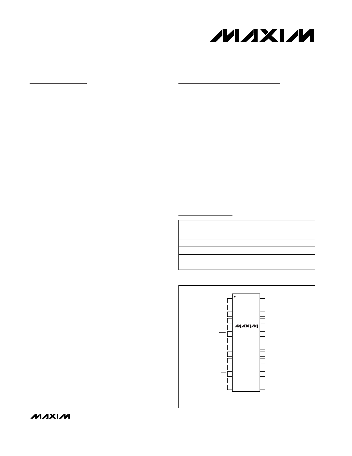
Ordering Information
19-3355; Rev 0; 8/04
For pricing, delivery, and ordering information, please contact Maxim/Dallas Direct! at
1-888-629-4642, or visit Maxim’s website at www.maxim-ic.com.
Quick-PWM and Dual Mode are trademarks of Maxim
Integrated Products, Inc.
Pin Configurations
Pin Configurations continued at end of data sheet.
PART TEMP RANGE
MAX8732EEI -40°C to +85°C 28 QSOP 200kHz/300kHz
MAX8733EEI -40°C to +85°C 28 QSOP 400kHz/500kHz
MAX8734EEI -40°C to +85°C 28 QSOP
PINPACKAGE
5V/3V
SWITCHING
FREQUENCY
200kHz/300kHz or
400kHz/500kHz
TOP VIEW
1
N.C.
2
PGOOD
3
ON3
4
ON5
5
ILIM3
SHDN
FB3
REF
FB5
PRO
ILIM5
SKIP
TON
BST5
MAX8734
6
7
8
9
10
11
12
13
14
QSOP
28
BST3
27
LX3
26
DH3
25
LDO3
24
DL3
23
GND
22
OUT3
21
OUT5
20
V+
19
DL5
18
LDO5
17
V
CC
16
DH5
15
LX5
MAX8732/MAX8733/MAX8734
High-Efficiency, Quad-Output, Main PowerSupply Controllers for Notebook Computers
2 _______________________________________________________________________________________
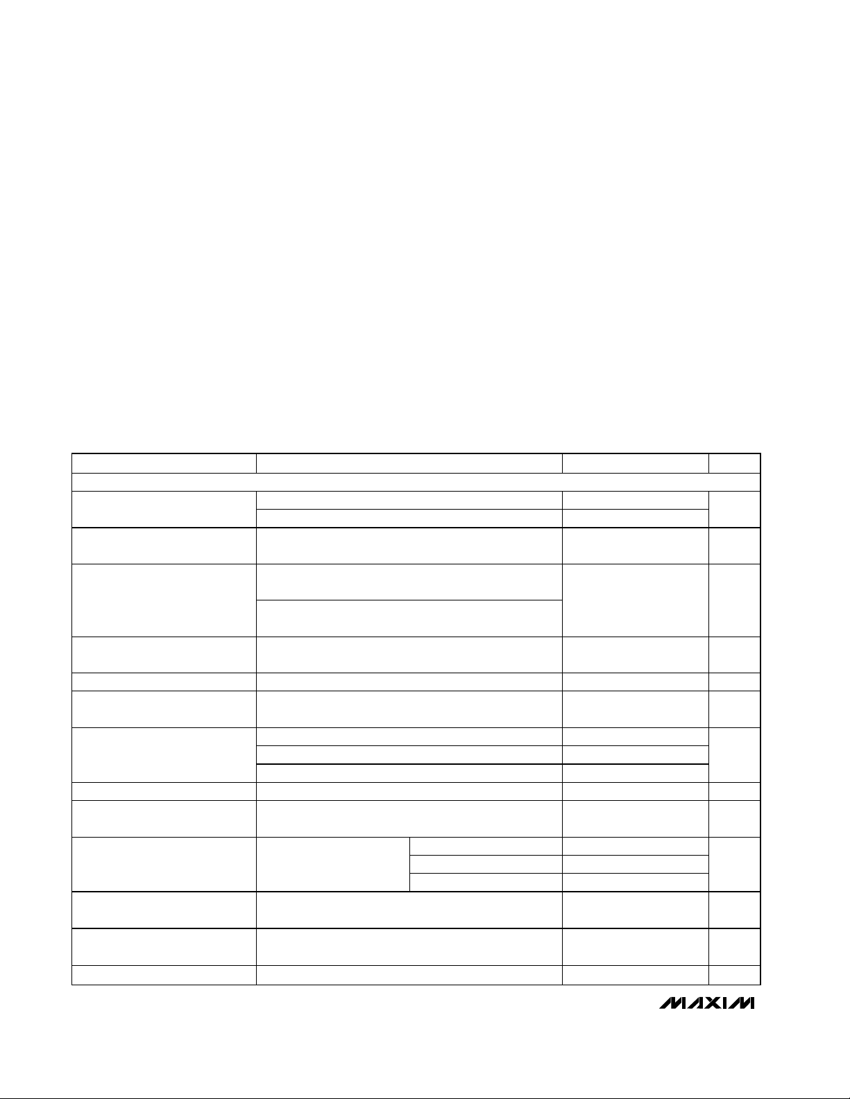
ABSOLUTE MAXIMUM RATINGS
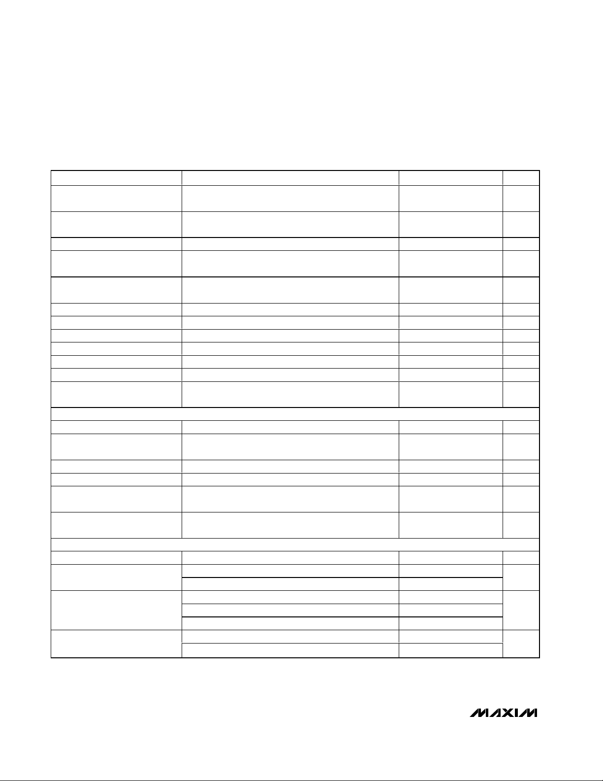
ELECTRICAL CHARACTERISTICS
(Circuit of Figure 1 and Figure 2, no load on LDO5, LDO3, OUT3, OUT5, and REF, V+ = 12V, ON3 = ON5 = VCC, V
SHDN
= 5V,
T
A
= 0°C to +85°C, unless otherwise noted. Typical values are at TA= +25°C.)
Stresses beyond those listed under “Absolute Maximum Ratings” may cause permanent damage to the device. These are stress ratings only, and functional
operation of the device at these or any other conditions beyond those indicated in the operational sections of the specifications is not implied. Exposure to
absolute maximum rating conditions for extended periods may affect device reliability.
V+, SHDN to GND..................................................-0.3V to +25V
BST_ to GND ..........................................................-0.3V to +30V
LX_ to BST_ ..............................................................-6V to +0.3V
CS_ to GND (MAX8732/MAX8733 only)......................-2V to +6V
V
CC
, LDO5, LDO3, OUT3, OUT5, ON3, ON5, REF,
FB3, FB5, SKIP, PRO, PGOOD to GND ...............-0.3V to +6V
DH3 to LX3 ..............................................-0.3V to (V
BST3
+ 0.3V)
DH5 to LX5 ..............................................-0.3V to (V
BST5
+ 0.3V)
ILIM3, ILIM5 to GND...................................-0.3V to (V
CC
+ 0.3V)
DL3, DL5 to GND....................................-0.3V to (V
LDO5
+ 0.3V)
TON to GND (MAX8734 only)...................................-0.3V to +6V
LDO3, LDO5, REF Short Circuit to GND ....................Momentary
LDO3 Current (Internal Regulator) Continuous ..............+100mA
LDO3 Current (Switched Over to OUT3) Continuous.....+200mA
LDO5 Current (Internal Regulator) Continuous ..............+100mA
LDO5 Current (Switched Over to OUT5) Continuous.....+200mA
Continuous Power Dissipation (T
A
= +70°C)
28-Pin QSOP (derate 10.8mW/°C above +70°C).........860mW
Operating Temperature Range ...........................-40°C to +85°C
Junction Temperature......................................................+150°C
Storage Temperature Range .............................-65°C to +150°C
Lead Temperature (soldering, 10s) .................................+300°C
MAIN SMPS CONTROLLERS
V+ Input Voltage Range
3.3V Output Voltage in
Fixed Mode
5V Output Voltage in Fixed Mode
Output Voltage in
Adjustable Mode
Output Voltage Adjust Range Either SMPS 2.0 5.5 V
FB3, FB5 Adjustable-Mode
Threshold Voltage
Line Regulation Either SMPS, 6V < V+ < 24V 0.005 %/V
Current-Limit Threshold
(Positive, Default)
Current-Limit Threshold
(Positive, Adjustable)
Zero-Current Threshold
Current-Limit Threshold
(Negative, Default)
Soft-Start Ramp Time Zero to full limit 1.7 ms
PARAMETER CONDITIONS MIN TYP MAX UNITS
LDO5 in regulation 6 24
V+ = LDO5, V
V+ = 6V to 24V, FB3 = GND, V
V+ = 6V to 24V, FB5 = GND, V
MAX8732/MAX8734 (TON = V
V+ = 7V to 24V, FB5 = GND, V
MAX8733/MAX8734 (TON = GND)
V+ = 6V to 24V, either SMPS 1.975 2.00 2.025 V
Dual-Mode comparator 0.1 0.2 V
Either SMPS, V
Either SMPS, SKIP = GND, 0 to 5A -1.5DC Load Regulation
Either SMPS, V
ILIM_ = VCC, GND - CS_ (MAX8732/MAX8733),
GND - LX_ (MAX8734)
GND - CS_
(MAX8732/MAX8733),
GND - LX_ (MAX8734)
SKIP = GND, ILIM_ = V
(MAX8732/MAX8733), GND - LX_ (MAX8734)
SKIP = ILIM_ = VCC, GND - CS_ (MAX8732/MAX8733),
GND - LX_ (MAX8734)
< 4.43V 4.5 5.5
OUT5
= 5V, 0 to 5A -0.1
SKIP
= 2V, 0 to 5A -1.7
SKIP
CC
= 5V 3.285 3.330 3.375 V
SKIP
= 5V,
SKIP
)
CC
= 5V,
SKIP
V
= 0.5V 40 50 60
ILIM_
V
= 1V 93 100 107
ILIM_
V
= 2V 185 200 215
ILIM_
, GND - CS_
4.975 5.050 5.125 V
93 100 107 mV
3mV
-120 mV
V
%
mV
MAX8732/MAX8733/MAX8734
High-Efficiency, Quad-Output, Main Power-
Supply Controllers for Notebook Computers
_______________________________________________________________________________________ 3
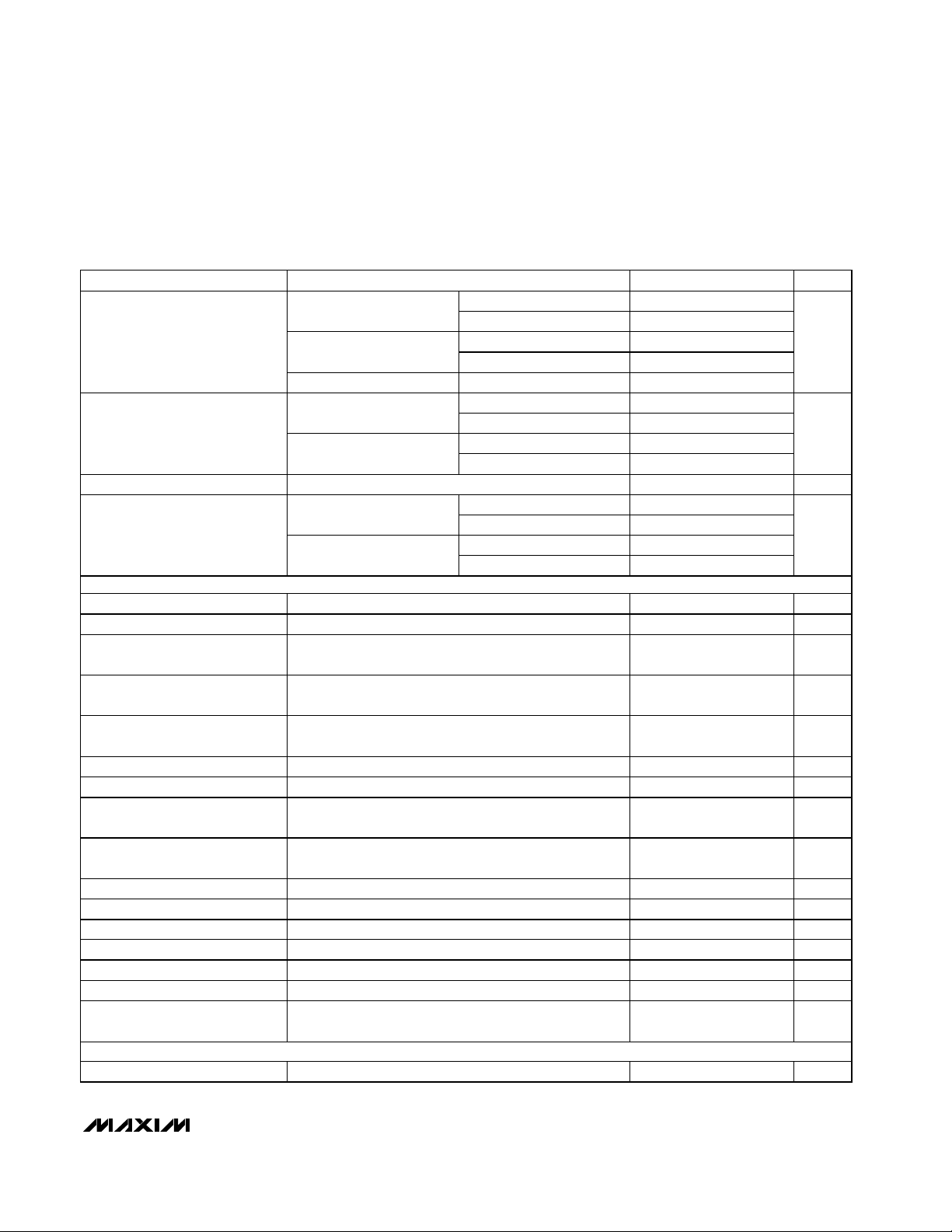
ELECTRICAL CHARACTERISTICS (continued)
(Circuit of Figure 1 and Figure 2, no load on LDO5, LDO3, OUT3, OUT5, and REF, V+ = 12V, ON3 = ON5 = VCC, V
SHDN
= 5V,
T
A
= 0°C to +85°C, unless otherwise noted. Typical values are at TA= +25°C.)
Operating Frequency
On-Time Pulse Width
Minimum Off-Time 250 300 350 ns
Maximum Duty Cycle
INTERNAL REGULATOR AND REFERENCE
LDO5 Output Voltage ON3 = ON5 = GND, 6V < V+ < 24V, 0 < I
LDO5 Short-Circuit Current LDO5 = GND 190 mA
LDO5 Undervoltage-Lockout
Fault Threshold
LDO5 Bootstrap Switch Threshold
LDO5 Bootstrap
Switch Resistance
LDO3 Output Voltage ON3 = ON5 = GND, 6V < V+ < 24V, 0 < I
LDO3 Short-Circuit Current LDO3 = GND 180 mA
LDO3 Bootstrap Switch Threshold
LDO3 Bootstrap Switch
Resistance
REF Output Voltage No external load 1.980 2.000 2.020 V
REF Load Regulation 0 < I
REF Sink Current REF in regulation 10 µA
V+ Operating Supply Current LDO5 switched over to OUT5, 5V SMPS 25 50 µA
V+ Standby Supply Current V+ = 6V to 24V, both SMPSs off, includes I
V+ Shutdown Supply Current V+ = 4.5V to 24V 6 15 µA
Quiescent Power Consumption
FAULT DETECTION
Overvoltage Trip Threshold FB3 or FB5 with respect to nominal regulation point +8 +11 +14 %
PARAMETER CONDITIONS MIN TYP MAX UNITS
MAX8732 or MAX8734
= 5V), SKIP = V
(V
TON
MAX8733 or MAX8734
= 0), SKIP = V
(V
TON
SKIP = REF 25 36
MAX8732 or MAX8734
(V
= 5V)
TON
MAX8733 or MAX8734
= 0)
(V
TON
MAX8732 or MAX8734
(V
= 5V)
TON
MAX8733 or MAX8734
= 0)
(V
TON
Falling edge of LDO5, hysteresis = 1% 3.7 4.0 4.3 V
Falling edge of OUT5, rising edge at OUT5 regulation
point
LDO5 to OUT5, V
Falling edge of OUT3, rising edge at OUT3 regulation
point
LDO3 to OUT3, V
< 50µA 10 mV
LOAD
Both SMPSs on, FB3 = FB5 = SKIP = GND, V
3.5V, V
OUT5
= 5.3V
CC 3.3V SMPS 500
OUT5
OUT3
5V SMPS 200
CC
3.3V SMPS 300
5V SMPS 400
V
= 5.05V 1.895 2.105 2.315
OUT5
V
= 3.33V 0.833 0.925 1.017
OUT3
V
= 5.05V 0.895 1.052 1.209
OUT5
V
= 3.33V 0.475 0.555 0.635
OUT3
V
= 5.05V 94
OUT5
V
= 3.33V 91
OUT3
V
= 5.05V 88
OUT5
V
= 3.33V 85
OUT3
< 100mA 4.90 5.00 5.10 V
LDO5
4.43 4.56 4.69 V
= 5V 1.4 3.2 Ω
< 100mA 3.28 3.35 3.42 V
LDO3
2.80 2.91 3.02 V
= 3.2V 1.5 3.5 Ω
SHDN
OUT3
=
150 250 µA
3 4.5 mW
kHz
µs
%

MAX8732/MAX8733/MAX8734
High-Efficiency, Quad-Output, Main PowerSupply Controllers for Notebook Computers
4 _______________________________________________________________________________________
ELECTRICAL CHARACTERISTICS (continued)
(Circuit of Figure 1 and Figure 2, no load on LDO5, LDO3, OUT3, OUT5, and REF, V+ = 12V, ON3 = ON5 = VCC, V
SHDN
= 5V,
T
A
= 0°C to +85°C, unless otherwise noted. Typical values are at TA= +25°C.)
Overvoltage Fault
Propagation Delay
PGOOD Threshold
PGOOD Propagation Delay Falling edge, 50mV overdrive 10 µs
PGOOD Output Low Voltage I
PGOOD Leakage Current High state, forced to 5.5V 1 µA
Thermal-Shutdown Threshold +160
Output Undervoltage
Shutdown Threshold
Output Undervoltage
Shutdown Blanking Time
INPUTS AND OUTPUTS
Feedback Input Leakage Current V
PRO Input Voltage
TON Input Voltage
Input Leakage Current
SHDN Input Trip Level
DH_ Gate-Driver
Sink/Source Current
DL_ Gate-Driver Source Current DL3 (source), DL5 (source), forced to 2V 1.7 A
DL_ Gate-Driver Sink Current DL3 (sink), DL5 (sink), forced to 2V 3.3 A
DH_ Gate-Driver On-Resistance BST - LX_ forced to 5V 1.5 4.0 Ω
DL_ Gate-Driver On-Resistance
PARAMETER CONDITIONS MIN TYP MAX UNITS
FB3 or FB5 delay with 50mV overdrive 10 µs
FB3 or FB5 with respect to nominal output, falling edge,
typical hysteresis = 1%
= 4mA 0.3 V
SINK
FB3 or FB5 with respect to nominal output voltage 65 70 75 %
From ON_ signal 10 22 35 ms
= V
FB3
Low level 0.6
High level 1.5
Low level 0.8
Float level 1.7 2.3SKIP Input Voltage
High level 2.4
Low level 0.8
High level 2.4
Clear fault level/SMPS off level 0.8
Delay start level 1.7 2.3ON3, ON5 Input Voltage
SMPS on level 2.4
V
PRO
V
ON_
V
SKIP
V
SHDN
V
CS_
V
ILIM3
Rising edge 1.2 1.6 2.0
Falling edge 0.96 1.00 1.04
DH3, DH5 forced to 2V 2 A
DL_, high state (pullup) 2.2 5.0
DL_, low state (pulldown) 0.6 1.5
= 2.2V -200 +40 +200 nA
FB5
or V
= 0 or 5V -2 +2
= 0 or 5V -1 +1
= 0 or 5V -2 +2
= 0 or 5V -1 +1
TON
= 0 or 24V -1 +1
, V
= 0 or 2V -0.2 +0.2
ILIM5
-12 -9.5 -7 %
o
C
V
V
V
V
µA
V
Ω
MAX8732/MAX8733/MAX8734
High-Efficiency, Quad-Output, Main Power-
Supply Controllers for Notebook Computers
_______________________________________________________________________________________ 5
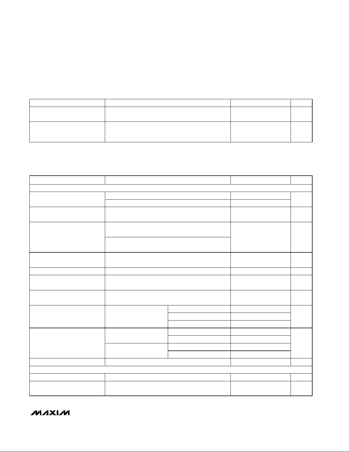
ELECTRICAL CHARACTERISTICS (continued)
(Circuit of Figure 1 and Figure 2, no load on LDO5, LDO3, OUT3, OUT5, and REF, V+ = 12V, ON3 = ON5 = VCC, V
SHDN
= 5V,
T
A
= 0°C to +85°C, unless otherwise noted. Typical values are at TA= +25°C.)
ELECTRICAL CHARACTERISTICS
(Circuit of Figure 1 and Figure 2, no load on LDO5, LDO3, OUT3, OUT5, and REF, V+ = 12V, ON3 = ON5 = VCC, V
SHDN
= 5V,
T
A
= -40°C to +85°C, unless otherwise noted.) (Note 1)
OUT3, OUT5 Discharge-Mode
On-Resistance
OUT3, OUT5 Discharge-Mode
Synchronous Rectifier
Turn-On Level
PARAMETER CONDITIONS MIN TYP MAX UNITS
12 40 Ω
0.2 0.3 0.4 V
MAIN SMPS CONTROLLERS
V+ Input Voltage Range
3.3V Output Voltage in
Fixed Mode
5V Output Voltage in Fixed Mode
Output Voltage in
Adjustable Mode
Output Voltage Adjust Range Either SMPS 2.0 5.5 V
FB3, FB5 Adjustable-Mode
Threshold Voltage
Current-Limit Threshold
(Positive, Default)
Current-Limit Threshold
(Positive, Adjustable)
On-Time Pulse Width
Minimum Off-Time 200 400 ns
INTERNAL REGULATOR AND REFERENCE
LDO5 Output Voltage ON3 = ON5 = GND, 6V < V+ < 24V, 0 < I
LDO5 Undervoltage-Lockout
Fault Threshold
PARAMETER CONDITIONS MIN TYP MAX UNITS
LDO5 in regulation 6 24
V+ = LDO5, V
V+ = 6V to 24V, FB3 = GND, V
V+ = 6V to 24V, FB5 = GND, V
MAX8732/MAX8734 (TON = V
V+ = 7V to 24V, FB5 = GND, V
MAX8733/MAX8734 (TON = GND)
V+ = 6V to 24V, either SMPS 1.97 2.03 V
Dual-Mode comparator 0.1 0.2 V
ILIM_ = VCC, GND - CS_ (MAX8732/MAX8733),
GND - LX_ (MAX8734)
GND - CS_
(MAX8732/MAX8733),
GND - LX_ (MAX8734)
MAX8732 or MAX8734
= 5V)
(V
TON
MAX8733 or MAX8734
= 0)
(V
TON
Falling edge of LDO5, hysteresis = 1% 3.7 4.3 V
< 4.41V 4.5 5.5
OUT5
= 5V 3.27 3.39 V
SKIP
= 5V,
SKIP
)
CC
= 5V,
SKIP
V
= 0.5V 40 60
ILIM_
V
= 1V 90 110
ILIM_
V
= 2V 180 220
ILIM_
V
= 5.05V 1.895 2.315
OUT5
V
= 3.33V 0.833 1.017
OUT3
V
= 5.05V 0.895 1.209
OUT5
V
= 3.33V 0.475 0.635
OUT3
< 100mA 4.90 5.10 V
LDO5
4.95 5.15 V
90 110 mV
V
mV
µs
MAX8732/MAX8733/MAX8734
High-Efficiency, Quad-Output, Main PowerSupply Controllers for Notebook Computers
6 _______________________________________________________________________________________
ELECTRICAL CHARACTERISTICS (continued)
(Circuit of Figure 1 and Figure 2, no load on LDO5, LDO3, OUT3, OUT5, and REF, V+ = 12.0.V, ON3 = ON5 = VCC, V
SHDN
= 5V,
T
A
= -40°C to +85°C, unless otherwise noted.) (Note 1)
LDO5 Bootstrap Switch Threshold
LDO5 Bootstrap Switch
Resistance
LDO3 Output Voltage ON3 = ON5 = GND, 6V < V+ < 24V, 0 < I
LDO3 Bootstrap Switch Threshold
LDO3 Bootstrap
Switch Resistance
REF Output Voltage No external load 1.975 2.025 V
REF Load Regulation 0 < I
REF Sink Current REF in regulation 10 µA
V+ Operating Supply Current LDO5 switched over to OUT5, 5V SMPS 50 µA
V+ Standby Supply Current V+ = 6V to 24V, both SMPSs off, includes I
V+ Shutdown Supply Current V+ = 4.5V to 24V 15 µA
Quiescent Power Consumption
FAULT DETECTION
Overvoltage Trip Threshold FB3 or FB5 with respect to nominal regulation point +8 +14 %
PGOOD Threshold
PGOOD Output Low Voltage I
PGOOD Leakage Current High state, forced to 5.5V 1 µA
Output Undervoltage Shutdown
Threshold
Output Undervoltage Shutdown
Blanking Time
INPUTS AND OUTPUTS
Feedback Input Leakage Current V
PRO Input Voltage
SKIP Input Voltage
TON Input Voltage
PARAMETER CONDITIONS MIN TYP MAX UNITS
Falling edge of OUT5, rising edge at OUT5 regulation
point
LDO5 to OUT5, V
Falling edge of OUT3, rising edge at OUT3 regulation
point
LDO3 to OUT3, V
< 50µA 10 mV
LOAD
Both SMPSs on, FB3 = FB5 = SKIP = GND, V
3.5V, V
FB3 or FB5 with respect to nominal output, falling edge,
typical hysteresis = 1%
SINK
FB3 or FB5 with respect to nominal output voltage 65 75 %
From ON_ signal 10 40 ms
FB3
Low level 0.6
High level 1.5
Low level 0.8
Float level 1.7 2.3
High level 2.4
Low level 0.8
High level 2.4
= 5.3V
OUT5
= 4mA 0.3 V
= V
= 2.2V -200 +200 nA
FB5
= 5V 3.2 Ω
OUT5
< 100mA 3.27 3.43 V
LDO3
= 3.2V 3.5 Ω
OUT3
SHDN
=
OUT3
4.43 4.69 V
2.80 3.02 V
300 µA
4.5 mW
-12 -7 %
V
V
V

MAX8732/MAX8733/MAX8734
High-Efficiency, Quad-Output, Main Power-
Supply Controllers for Notebook Computers
_______________________________________________________________________________________ 7
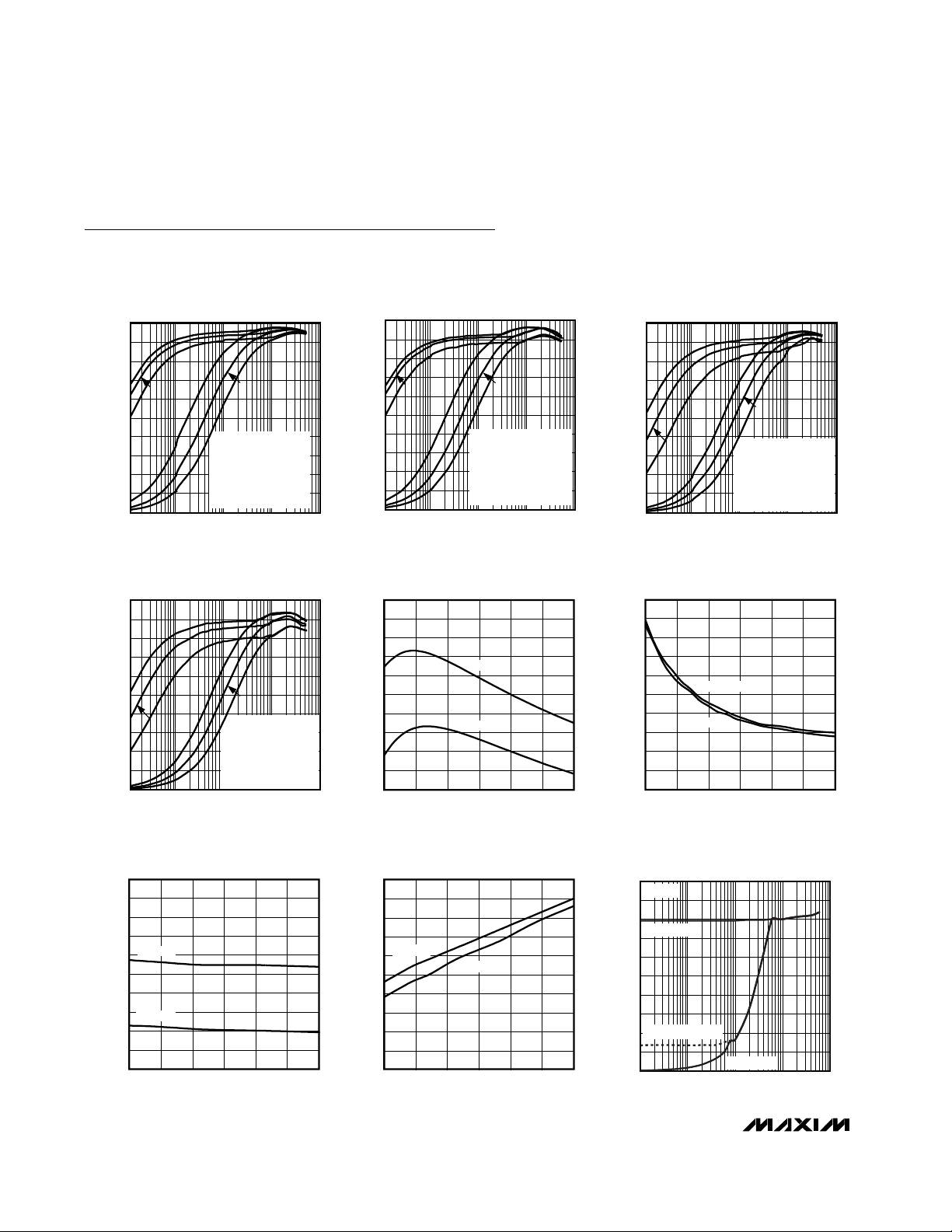
ELECTRICAL CHARACTERISTICS (continued)
(Circuit of Figure 1 and Figure 2, no load on LDO5, LDO3, OUT3, OUT5, and REF, V+ = 12.0.V, ON3 = ON5 = VCC, V
SHDN
= 5V,
T
A
= -40°C to +85°C, unless otherwise noted.) (Note 1)
Note 1: Specifications to -40°C are guaranteed by design, not production tested.
Input Leakage Current
SHDN Input Trip Level
DH_ Gate-Driver On-Resistance BST - LX_ forced to 5V 4.0 Ω
DL_ Gate-Driver On-Resistance
OUT3, OUT5 Discharge-Mode
On-Resistance
OUT3, OUT5 Discharge-Mode
Synchronous Rectifier
Turn-On Level
PARAMETER CONDITIONS MIN TYP MAX UNITS
Clear fault level/SMPS off level 0.8
Delay start level 1.7 2.3ON3, ON5 Input Voltage
SMPS on level 2.4
V
or V
PRO
V
= 0 or 5V -1 +1
ON_
V
= 0 or 5V -2 +2
SKIP
V
SHDN
V
= 0 or 5V -2 +2
CS_
V
ILIM3
Rising edge 1.2 2.0
Falling edge 0.96 1.04
DL_, high state (pullup) 5.0
DL_, low state (pulldown) 1.5
= 0 or 5V -1 +1
TON
= 0 or 24V -1 +1
, V
= 0 or 2V -0.2 +0.2
ILIM5
0.2 0.4 V
40 Ω
V
µA
V
Ω
MAX8732/MAX8733/MAX8734
High-Efficiency, Quad-Output, Main PowerSupply Controllers for Notebook Computers
8 _______________________________________________________________________________________
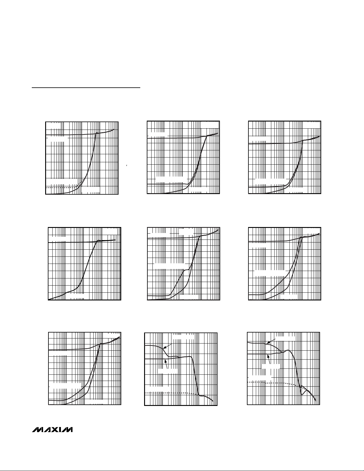
Typical Operating Characteristics
(Circuit of Figure 1 and Figure 2, no load on LDO5, LDO3, OUT3, OUT5, and REF, V+ = 12V, ON3 = ON5 = VCC, SHDN = V+,
R
CS
= 7mΩ, V
ILIM
_ = 0.5V, TA= +25°C, unless otherwise noted.)
100
0
0.001 0.01 0.1 1 10
5V OUTPUT EFFICIENCY
vs. LOAD CURRENT (MAX8732)
20
MAX8732/3/4 toc01
LOAD CURRENT (A)
EFFICIENCY (%)
40
60
80
70
50
30
10
90
A: IDLE MODE, VIN = 7V
B: IDLE MODE, V
IN
= 12V
C: IDLE MODE, V
IN
= 24V
D: PWM MODE, V
IN
= 7V
E: PWM MODE, V
IN
= 12V
F: PWM MODE, V
IN
= 24V
A
B
C
D
E
F
100
0
0.001 0.01 0.1 1 10
5V OUTPUT EFFICIENCY
vs. LOAD CURRENT (MAX8733)
20
MAX8732/3/4 toc02
LOAD CURRENT (A)
EFFICIENCY (%)
40
60
80
70
50
30
10
90
A: IDLE MODE, VIN = 7V
B: IDLE MODE, V
IN
= 12V
C: IDLE MODE, V
IN
= 24V
D: PWM MODE, V
IN
= 7V
E: PWM MODE, V
IN
= 12V
F: PWM MODE, V
IN
= 24V
A
B
C
D
E
F
100
0
0.001 0.01 0.1 1 10
3.3V OUTPUT EFFICIENCY
vs. LOAD CURRENT (MAX8732)
20
MAX8732/3/4 toc03
LOAD CURRENT (A)
EFFICIENCY (%)
40
60
80
70
50
30
10
90
A: IDLE MODE, VIN = 7V
B: IDLE MODE, V
IN
= 12V
C: IDLE MODE, V
IN
= 24V
D: PWM MODE, V
IN
= 7V
E: PWM MODE, V
IN
= 12V
F: PWM MODE, V
IN
= 24V
A
B
C
D
E
F
100
0
0.001 0.01 0.1 1 10
3.3V OUTPUT EFFICIENCY
vs. LOAD CURRENT (MAX8733)
20
MAX8732/3/4 toc04
LOAD CURRENT (A)
EFFICIENCY (%)
40
60
80
70
50
30
10
90
A: IDLE MODE, VIN = 7V
B: IDLE MODE, V
IN
= 12V
C: IDLE MODE, V
IN
= 24V
D: PWM MODE, V
IN
= 7V
E: PWM MODE, V
IN
= 12V
F: PWM MODE, V
IN
= 24V
A
B
C
D
E
F
20
26
24
22
30
28
38
36
34
32
40
7
10 13 16 19
22
25
PWM NO-LOAD BATTERY CURRENT
vs. INPUT VOLTAGE
MAX8732/3/4 toc05
INPUT VOLTAGE (V)
BATTERY CURRENT (mA)
MAX8733
MAX8732
0.10
0.19
0.16
0.13
0.25
0.22
0.37
0.34
0.31
0.28
0.40
7101316192225
IDLE MODE™ NO-LOAD BATTERY CURRENT
vs. INPUT VOLTAGE
MAX8732/3/4 toc06
INPUT VOLTAGE (V)
BATTERY CURRENT (mA)
MAX8733
MAX8732
170
176
174
172
180
178
188
186
184
182
190
7101316192225
STANDBY INPUT CURRENT
vs. INPUT VOLTAGE
MAX8732/3/4 toc07
INPUT VOLTAGE (V)
STANDBY INPUT CURRENT (µA)
MAX8732
MAX8733
5.0
6.5
6.0
5.5
7.5
7.0
9.5
9.0
8.5
8.0
10.0
7101316192225
SHUTDOWN INPUT CURRENT
vs. INPUT VOLTAGE
MAX8732/3/4 toc08
INPUT VOLTAGE (V)
SHUTDOWN INPUT CURRENT (µA)
MAX8733
MAX8732
5V OUTPUT SWITCHING FREQUENCY
vs. LOAD CURRENT (MAX8732)
MAX8732/3/4 toc09
LOAD CURRENT (A)
SWITCHING FREQUENCY (kHz)
10.10.01
25
50
75
100
125
150
175
200
225
250
0
0.001 10
VIN = 7V
PWM MODE
PFM MODE
ULTRASONIC MODE
Idle Mode is a trademark of Maxim Integrated Products, Inc.
MAX8732/MAX8733/MAX8734
High-Efficiency, Quad-Output, Main Power-
Supply Controllers for Notebook Computers
_______________________________________________________________________________________ 9
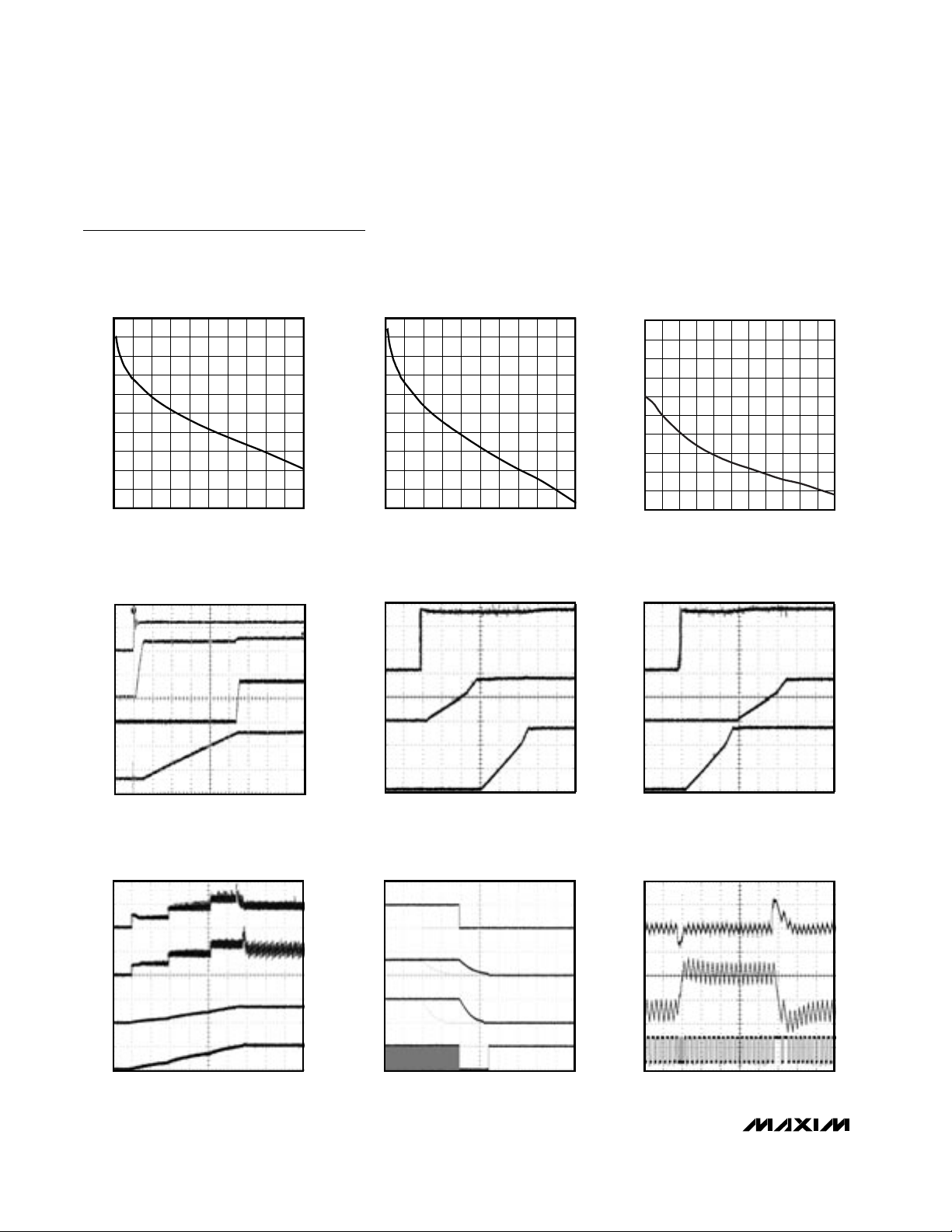
Typical Operating Characteristics (continued)
(Circuit of Figure 1 and Figure 2, no load on LDO5, LDO3, OUT3, OUT5, and REF, V+ = 12V, ON3 = ON5 = VCC, SHDN = V+,
R
CS
= 7mΩ, V
ILIM
_ = 0.5V, TA= +25°C, unless otherwise noted.)
3.3V OUTPUT SWITCHING FREQUENCY
vs. LOAD CURRENT (MAX8732)
MAX8732/3/4 toc10
LOAD CURRENT (A)
SWITCHING FREQUENCY (kHz)
10.10.01
40
80
120
160
200
240
280
320
360
0
0.001 10
VIN = 7V
PWM MODE
PFM MODE
ULTRASONIC MODE
250
0
0.001 0.01 0.1 1 10
5V OUTPUT SWITCHING
FREQUENCY vs. LOAD CURRENT (MAX8732)
50
MAX8732/3/4 toc11
LOAD CURRENT (A)
SWITCHING FREQUENCY (kHz)
100
150
200
175
125
75
25
225
PWM MODE
PFM MODE
VIN = 24V
ULTRASONIC MODE
400
0
0.001 0.01 0.1 1 10
3.3V OUTPUT SWITCHING
FREQUENCY vs. LOAD CURRENT (MAX8732)
80
MAX8732/3/4 toc12
LOAD CURRENT (A)
SWITCHING FREQUENCY (kHz)
160
240
320
280
200
120
40
360
PWM MODE
PFM MODE
VIN = 24V
ULTRASONIC MODE
500
0
0.001 0.01 0.1 1 10
5V OUTPUT SWITCHING
FREQUENCY vs. LOAD CURRENT (MAX8733)
100
MAX8732/3/4 toc13
LOAD CURRENT (A)
SWITCHING FREQUENCY (kHz)
200
300
400
350
250
150
50
450
PWM MODE
IDLE MODE
VIN = 7V
110
0
100
200
400
300
500
600
0.001 0.01 0.1
3.3V OUTPUT SWITCHING
FREQUENCY vs. LOAD CURRENT (MAX8733)
MAX8732/3/4 toc14
LOAD CURRENT (A)
SWITCHING FREQUENCY (kHz)
550
450
350
250
150
50
PWM MODE
PFM MODE
VIN = 7V
ULTRASONIC MODE
500
0
0.001 0.01 0.1 1 10
5V OUTPUT SWITCHING
FREQUENCY vs. LOAD CURRENT (MAX8733)
100
MAX8732/3/4 toc15
LOAD CURRENT (A)
SWITCHING FREQUENCY (kHz)
200
300
400
350
250
150
50
450
PWM MODE
PFM MODE
VIN = 24V
ULTRASONIC MODE
110
0
100
200
400
300
500
600
0.001 0.01 0.1
3.3V OUTPUT SWITCHING
FREQUENCY vs. LOAD CURRENT (MAX8733)
MAX8732/3/4 toc16
LOAD CURRENT (A)
SWITCHING FREQUENCY (kHz)
550
450
350
250
150
50
PWM MODE
IDLE MODE
VIN = 24V
ULTRASONIC MODE
OUT5 VOLTAGE REGULATION
vs. LOAD CURRENT (MAX8732)
MAX8732/3/4 toc17
LOAD CURRENT (A)
OUTPUT VOLTAGE (V)
10.10.01
5.07
5.09
5.11
5.13
5.15
5.17
5.19
5.05
0.001 10
ULTRASONIC
IDLE MODE
FORCED-PWM
OUT3 VOLTAGE REGULATION
vs. LOAD CURRENT (MAX8732)
MAX8732/3/4 toc18
LOAD CURRENT (A)
OUTPUT VOLTAGE (V)
10.10.01
3.34
3.35
3.36
3.37
3.38
3.39
3.41
3.40
3.33
0.001 10
ULTRASONIC
IDLE MODE
FORCED-PWM
MAX8732/MAX8733/MAX8734
High-Efficiency, Quad-Output, Main PowerSupply Controllers for Notebook Computers
10 ______________________________________________________________________________________
Typical Operating Characteristics (continued)
(Circuit of Figure 1 and Figure 2, no load on LDO5, LDO3, OUT3, OUT5, and REF, V+ = 12V, ON3 = ON5 = VCC, SHDN = V+,
R
CS
= 7mΩ, V
ILIM
_ = 0.5V, TA= +25°C, unless otherwise noted.)
4.95
4.96
4.97
4.98
4.99
5.00
020304010 50 60 70 9080 100
LDO5 REGULATOR OUTPUT VOLTAGE
vs. OUTPUT CURRENT
MAX8732/3/4 toc19
LDO5 OUTPUT CURRENT (mA)
LDO5 OUTPUT VOLTAGE (V)
3.330
3.334
3.332
3.338
3.336
3.342
3.340
3.344
3.348
3.346
3.350
020304010 50 60 70 9080 100
LDO3 REGULATOR OUTPUT VOLTAGE
vs. OUTPUT CURRENT
MAX8732/3/4 toc20
LDO3 OUTPUT CURRENT (mA)
LDO3 OUTPUT VOLTAGE (V)
1.995
1.997
1.996
2.000
1.999
1.998
2.001
2.002
2.004
2.003
2.005
-10 10 20030405060708090100
REFERENCE VOLTAGE
vs. OUTPUT CURRENT
MAX8732/3/4 toc21
I
REF
(µA)
V
REF
(V)
0
0
0
10V
REF, LDO3, AND LDO5 POWER-UP
MAX8732/3/4 toc22
400µs/div
V+
10V/div
LDO5
2V/div
LDO3
2V/div
REF
1V/div
0
0
5V
0
3.3V
0
5V
DELAYED START WAVEFORMS
(ON5 = REF)
MAX8732/3/4 toc23
200µs/div
ON5
2V/div
OUT3
2V/div
OUT5
2V/div
0
5V
0
3.3V
0
5V
DELAYED START WAVEFORMS
(ON3 = REF)
MAX8732/3/4 toc24
200µs/div
ON3
2V/div
OUT3
2V/div
OUT5
2V/div
0
5A
0
3.3V
0
5A
SOFT-START WAVEFORMS
MAX8732/3/4 toc25
200µs/div
I
L5
5A/div
OUT3
5V/div
OUT5
5V/div
I
L3
5A/div
0
5V
0
3.3V
0
5V
0
5V
SHUTDOWN WAVEFORMS
MAX8732/3/4 toc26
10ms/div
ON3
5V/div
OUT5
5V/div
DL3
5V/div
OUT3
5V/div
0
5V
SWITCHING
0
4A
1A
5V
MAX8732/MAX8734 (TON = VCC)
5V PWM-MODE
LOAD TRANSIENT RESPONSE
MAX8732/3/4 toc27
20µs/div
V
OUT
,
ACCOUPLED
100mV/div
INDUCTOR
CURRENT
2A/div
DL5
5V/div
5V
 Loading...